
NTE932
Integrated Circuit
3≠Terminal Positive Voltage Regulator
5V, 5A
Description:
The NTE932 is a 3≠terminal fixed positive voltage regulator in a TO3 type package designed for use
in applications requiring a well regulated positive output voltage. Outstanding features include full
power usage up to 5A of load current, internal current limiting, thermal shutdown, and safe area
protection on the chip, providing protection o he series pass Darlington, under most operating condi-
tions. A low≠noise, temperature stable band gap reference is the key design factor insuring excellent
temperature regulation. This, coupled to a very low output impedance, insures superior load regula-
tion.
Features:
D
Guaranteed Power Dissipation: 50W @ T
C
= +80
∞
C
D
Guaranteed Input≠Output Differential
D
Low Noise, Band Gap Reference
D
Remote Sense Capability
D
Sample Power Cycled Burn≠In
D
Guaranteed Thermal Resistance, Junction≠to≠Case: 0.9
∞
C/W
Absolute Maximum Ratings:
Input Voltage (Note 1), V
IN
30V
. . . . . . . . . . . . . . . . . . . . . . . . . . . . . . . . . . . . . . . . . . . . . . . . . . . . . . . . . .
Power Dissipation, P
D
Internally Limited
. . . . . . . . . . . . . . . . . . . . . . . . . . . . . . . . . . . . . . . . . . . . . . . . . .
Derates Above 80
∞
C
1.111W/
∞
C
. . . . . . . . . . . . . . . . . . . . . . . . . . . . . . . . . . . . . . . . . . . . . . . . . . . .
Operating Junction Temperature Range, T
J
≠55
∞
to +150
∞
C
. . . . . . . . . . . . . . . . . . . . . . . . . . . . . . . . . .
Storage Temperature Range, T
stg
≠65
∞
to +150
∞
C
. . . . . . . . . . . . . . . . . . . . . . . . . . . . . . . . . . . . . . . . . .
Typical Thermal Resistance, Junction≠to≠Case, R
thJC
0.9
∞
C/W
. . . . . . . . . . . . . . . . . . . . . . . . . . . . . .
Lead Temperature (Soldering, 60sec), T
L
+300
∞
C
. . . . . . . . . . . . . . . . . . . . . . . . . . . . . . . . . . . . . . . . . . .
Burn≠In In Thermal Limit
100%
. . . . . . . . . . . . . . . . . . . . . . . . . . . . . . . . . . . . . . . . . . . . . . . . . . . . . . . . . .
Note 1. Short circuit protection is only assured to V
IN
max. In case of short circuit, with input≠output
voltages approaching V
IN
max, regulator may require the removal of the input voltage to restart.
Electrical Characteristics: (T
J
= 0
∞
to +125
∞
C unless otherwise specified)
Parameter
Symbol
Test Conditions
Min
Typ
Max
Unit
Output Voltage
V
O
T
J
= +25
∞
C, V
IN
= 8V to 15V, I
O
= 10mA to 5A,
Note 2
4.75
5.00
5.25
V
Input≠Output Voltage
Differential
V
IN
≠V
O
I
O
= 5A
2.6
≠
≠
V
Line Regulation
Reg
line
T
J
= +25
∞
C, V
IN
= 8V to 20V, I
O
= 3A, Note 3
≠
≠
1.0
%/V
O
Load Regulation
Reg
load
T
J
= +25
∞
C, V
IN
= 8V, I
O
= 10mA to 5A, Note 3
≠
≠
0.6
%/V
O
Quiescent Current
I
Q
T
J
= +25
∞
C, V
IN
= 8V, I
O
= 10mA
≠
≠
25
mA
Quiescent Current, Line
I
Q(Line)
T
J
= +25
∞
C, V
IN
= 8V to 15V, I
O
= 10mA
≠
≠
5
mA
Quiescent Current, Load
I
Q(Load)
T
J
= +25
∞
C, V
IN
= 8V, I
O
= 10mA to 5A
≠
≠
5
mA
Current Limit
I
LIM
T
J
= +25
∞
C, V
IN
= 10V, Note 2
≠
≠
15
A
Temperature Coefficient
T
C
V
IN
= 8V, I
O
= 100mA
≠
≠
5
mA
Output Noise Voltage
V
n
V
IN
= 8V, I
O
= 100mA, f = 10Hz to 100kHz
≠
≠
10
µ
V
rms
Ripple Attenuation
R
A
V
IN
= 10V, I
O
= 2A
60
≠
≠
dB
Power Dissipation
P
D
2.6V to 10V (V
IN
≠ V
O
), I
O
= 10mA to 5A
≠
≠
50
W
Note 2. Low duty cycle pulse testing with Kelvin connections required. Die temperature changes
must be accounted for separately.
Note 3. Ripple attenuation is specified for a 1V
rms
, 120Hz, input ripple. Ripple attenuation is
minimum of 60dB at 5V output and is 1dB less for each volt increase in the output volt-
age.
Note 4. V
O
= V
C
(1 + R1/R2) where:
R1 = Resistance from output to control
R2 = Resistance from control to common
Output
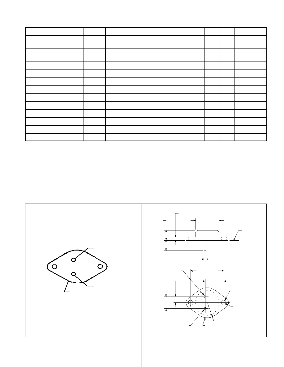
Input
Case/GND
2
1
1.187 (30.16)
.875 (22.2)
Dia Max
.665
(16.9)
.430
(10.92)
Seating
Plane
.040 (1.02)
.312 (7.93) Min
.135 (3.45) Max
.350 (8.89)
V
OUT
GND/Case
V
IN
.215 (5.45)
.525 (13.35) R Max
.156 (3.96) Dia
(2 Holes)
.188 (4.8) R Max
Pin Connection Diagram