NTE944 & NTE944M
Integrated Circuit
Programmable Operational Amplifier
Description:
The NTE944 (8≠Lead Metal Can) and NTE944M (8≠Lead MiniDIP) are extremely versatile program-
mable monolithic operational amplifiers. A single external master bias current setting resistor programs
the input bias current, input offset current, quiescent power consumption, slew rate, input noise, and the
gain≠bandwidth product. These devices are truly general purpose operational amplifiers.
Features:
D
±
1V to
±
18V power supply operation
D
3nA input offset current
D
Standby power consumption as low as 500mW
D
No frequency compensation required
D
Programmable electrical characteristics
D
Offset voltage nulling capability
D
Can be powered by two flashlight batteries
D
Short circuit protection
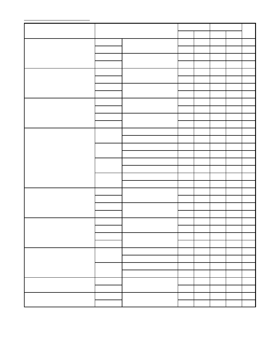
Absolute Maximum Ratings:
Supply Voltage
±
18V
. . . . . . . . . . . . . . . . . . . . . . . . . . . . . . . . . . . . . . . . . . . . . . . . . . . . . . . . . . . . . . . . . . . .
Power Dissipation (Note 1)
500mW
. . . . . . . . . . . . . . . . . . . . . . . . . . . . . . . . . . . . . . . . . . . . . . . . . . . . . .
Differential Input Voltage
±
30V
. . . . . . . . . . . . . . . . . . . . . . . . . . . . . . . . . . . . . . . . . . . . . . . . . . . . . . . . . . .
Input Voltage (Note 2)
±
15V
. . . . . . . . . . . . . . . . . . . . . . . . . . . . . . . . . . . . . . . . . . . . . . . . . . . . . . . . . . . . . .
I
SET
Current
150
µ
A
. . . . . . . . . . . . . . . . . . . . . . . . . . . . . . . . . . . . . . . . . . . . . . . . . . . . . . . . . . . . . . . . . . . . .
Output Short Circuit Duration
Indefinite
. . . . . . . . . . . . . . . . . . . . . . . . . . . . . . . . . . . . . . . . . . . . . . . . . . .
Operating Temperature Range
0
∞
T
A
+70
∞
C
. . . . . . . . . . . . . . . . . . . . . . . . . . . . . . . . . . . . . . . . . . . .
Storage Temperature Range
≠65
∞
to +150
∞
C
. . . . . . . . . . . . . . . . . . . . . . . . . . . . . . . . . . . . . . . . . . . . . . .
Lead Temperature (Soldering, 10sec)
+300
∞
C
. . . . . . . . . . . . . . . . . . . . . . . . . . . . . . . . . . . . . . . . . . . . . .
Note 1. The maximum junction temperature of the NTE944 is 100
∞
C. For operating at elevated tem-
peratures, the NTE944 must be derated based on a thermal resistance of 150
∞
C/W junction
to ambient, or 45
∞
C/W junction to case. The thermal resistance of the NTE944M is +125
∞
C/W.
Note 2. For supply voltages less than
±
15V, the absolute maximum input voltage is equal to the supply
voltage.