
NTE56028
TRIAC, 40 Amp
Description:
The NTE56028 is a 40 Amp TRIAC is a TO220 type package designed primarily for full≠wave AC con-
trol applications such as lighting systems, heater controls, motor controls, and power supplies.
Features:
D
Blocking Voltage of 800V
D
All Diffused and Glass≠Passivated Junctions for Parameter Uniformity and Stability
D
Gate Triggering Guaranteed in Four Modes
Absolute Maximum Ratings:
Peak Repetitive Off≠State Voltage, V
DRM
(T
J
= ≠40
∞
to +125
∞
C, 1/2 Sine Wave 50 to 60Hz, Gate Open, Note 1)
800V
. . . . . . . . . . . . .
On≠State RMS Current (T
C
= +75
∞
C, Full Cycle Sine Wave 50 to60Hz, Note 2), I
T
(RMS)
40A
. . . .
Peak Non≠Repetitive Surge Current (T
J
= +125
∞
C, One Full Cycle, 60Hz), I
TSM
350A
. . . . . . . . . . .
Circuit Fusing (t = 8.3ms), I
2
t
500A
2
s
. . . . . . . . . . . . . . . . . . . . . . . . . . . . . . . . . . . . . . . . . . . . . . . . . . . . .
Peak Gate Current (t
2
µ
s), I
GM
±
2A
. . . . . . . . . . . . . . . . . . . . . . . . . . . . . . . . . . . . . . . . . . . . . . . . . . . . .
Peak Gate Voltage (t
2
µ
s), V
GM
±
10V
. . . . . . . . . . . . . . . . . . . . . . . . . . . . . . . . . . . . . . . . . . . . . . . . . . .
Peak Gate Power (t
2
µ
s), P
GM
20W
. . . . . . . . . . . . . . . . . . . . . . . . . . . . . . . . . . . . . . . . . . . . . . . . . . . .
Average Gate Power (T
C
= +75
∞
C, t
8.3ms), P
G(AV)
0.5W
. . . . . . . . . . . . . . . . . . . . . . . . . . . . . . . . . .
Operating Junction Temperature Range, T
J
≠40
∞
to +125
∞
C
. . . . . . . . . . . . . . . . . . . . . . . . . . . . . . . . . .
Storage Temperature Range, T
stg
≠40
∞
to +150
∞
C
. . . . . . . . . . . . . . . . . . . . . . . . . . . . . . . . . . . . . . . . . .
Thermal Resistance, Junction≠to≠Case, R
thJC
1
∞
C/W
. . . . . . . . . . . . . . . . . . . . . . . . . . . . . . . . . . . . . . .
Thermal Resistance, Junction≠to≠Ambient, R
thJA
60
∞
C/W
. . . . . . . . . . . . . . . . . . . . . . . . . . . . . . . . . . . .
Mounting Torque
8in. lb.
. . . . . . . . . . . . . . . . . . . . . . . . . . . . . . . . . . . . . . . . . . . . . . . . . . . . . . . . . . . . . . . . .
Note 1. Ratings apply for open gate conditions. Devices shall not be tested with a constant current
source for blocking voltage such that the voltage applied exceeds the rated blocking voltage.
Note 2. This device is rated for use in applications subject to high surge conditions. Care must be
taken to insure proper heat sinking when the device is to be used at high sustained currents.
Electrical Characteristics: (T
C
= +25
∞
C and either polarity of MT
1
to MT
2
voltage unless
otherwise specified)
Parameter
Symbol
Test Conditions
Min
Typ
Max
Unit
Peak Forward Blocking Current
I
DRM
V
DRM
= 800V, T
J
= +25
∞
C
≠
≠
10
µ
A
V
DRM
= 800V, T
J
= +125
∞
C
≠
≠
2
mA
Peak Reverse Blocking Current
I
RRM
V
RRM
= 800V, T
J
= +25
∞
C
≠
≠
10
µ
A
V
RRM
= 800V, T
J
= +125
∞
C
≠
≠
2
mA
Peak On≠State Voltage
V
TM
I
TM
= 56A (Peak), Note 3
≠
1.40
1.85
V
Gate Trigger Current (Continuous DC)
MT
2
(+), G (+); MT
2
(≠), G (≠);
MT
2
(+), G (≠)
I
GT
V
D
= 12V, R
L
= 100
,
≠
25
50
mA
MT
2
(≠), G (+)
≠
40
75
mA
Gate Trigger Voltage (Continuous DC)
MT
2
(+), G (+); MT
2
(≠), G (≠);
MT
2
(+), G (≠)
V
GT
V
D
= 800V, R
L
= 100
,
≠
1.1
2.0
V
MT
2
(≠), G (+)
≠
1.3
2.5
V
Gate Non≠Trigger Voltage
MT
2
(+), G (+); MT
2
(≠), G (≠);
MT
2
(+), G (≠)
V
GD
V
D
= 800V, T
J
= +125
∞
C, R
L
= 10k,
0.2
≠
≠
V
MT
2
(≠), G (+)
0.2
≠
≠
V
Holding Current
I
H
V
D
= 12V, Gate Open
≠
30
75
mA
Gate Controlled Turn≠On Time
t
gt
V
D
= 800V, I
TM
= 56A (Peak),
I
GT
= 200mA
≠
1.5
≠
µ
s
Critical Rate of Rise of Off≠State
Voltage
dv/dt
V
D
= 800V, Exponential Waveform,
T
C
= +125
∞
C
≠
50
≠
V/
µ
s
Critical Rate 0f Rise of Commutation
Voltage
dv/dt(c)
V
D
= 800V, I
TM
= 56A (Peak),
Commutating di/dt = 13.4A/ms,
Gate Unenergized, T
C
= +75
∞
C
≠
5
≠
V/
µ
s
Note 3. Pulse Width
2ms, Duty Cycle
2%.
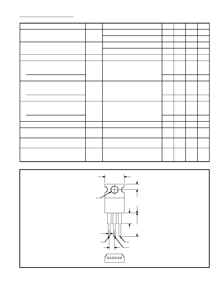
.250 (6.35)
Max
.500
(12.7)
Max
.500
(12.7)
Min
.110 (2.79)
.420 (10.67)
Max
.070 (1.78) Max
MT
1
.100 (2.54)
MT
2
/Tab
Gate
.147 (3.75)
Dia Max