
NTE978/NTE978C/NTE978SM
Integrated Circuit
Dual Timer
Description:
The NTE978 series dual timing circuit is a highly stable controller capable of producing accurate time
delays or oscillation. The NTE978 is a dual NTE955. Timing is provided by an external resistor and
capacitor for each timing function. The two timers operate independently of each other sharing only
V
CC
and GND. The circuits may be triggered and reset on falling waveforms. The output structures
may sink or source 200mA.
Features:
D
Direct Replacement for 556 Timers
D
Replaces Two 555 Timers
D
Timing from Microseconds through Hours
D
Operates in both Astable and Monostable Modes
D
Adjustable Duty Cycle
D
Output can Source or Sink 200mA
D
Output and Supply TTL Compatible
D
Temperature Stability better than 0.005% per
∞
C
D
Normally On and Normally Off Output
D
Available in Three Types:
NTE978
14≠Lead DIP
NTE978C
14≠Lead DIP (CMOS)
NTE978SM SOIC≠14 (Surface Mount)
Applications:
D
Precision Timing
D
Pulse Generation
D
Sequential Timing
D
Time Delay Generation
D
Pulse Width Modulation
D
Pulse Position Modulation
D
Linear Ramp Generator
Absolute Maximum Ratings:
Supply Voltage, V
CC
+18V
. . . . . . . . . . . . . . . . . . . . . . . . . . . . . . . . . . . . . . . . . . . . . . . . . . . . . . . . . . . . . . .
Power Dissipation (Note 1), P
D
1620mW
. . . . . . . . . . . . . . . . . . . . . . . . . . . . . . . . . . . . . . . . . . . . . . . . . .
Operating Temperature Range, T
A
0
∞
to +70
∞
C
. . . . . . . . . . . . . . . . . . . . . . . . . . . . . . . . . . . . . . . . . . . . .
Storage Temperature Range, T
stg
≠65
∞
to +150
∞
C
. . . . . . . . . . . . . . . . . . . . . . . . . . . . . . . . . . . . . . . . . .
Lead Temperature (During Soldering, 10sec Max), T
L
+260
∞
C
. . . . . . . . . . . . . . . . . . . . . . . . . . . . . . . .
Note 1. For operating at elevated temperaturesthe device must be derated based on a +150
∞
C maxi-
mum junction temperature and a thermal resistance of +77
∞
C/W for NTE978 and NTE978C
and +110
∞
C/W for NTE978SM.
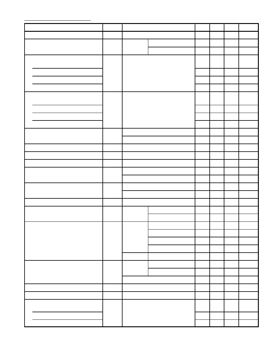
Electrical Characteristics: (T
A
= +25
∞
C, V
CC
= +5V to +15V, unless otherwise specified)
Parameter
Symbol
Test Conditions
Min
Typ
Max
Unit
Supply Voltage
V
CC
4.5
≠
16
V
Supply Current (Each Timer Section)
I
CC
Low State,
V
CC
= 5V, R
L
=
≠
3
6
mA
Note 2
V
CC
= 15V, R
L
=
≠
10
14
mA
Timing Error, Monostable
Initial Accuracy
≠
0.75
≠
%
Drift with Temperature
R
A
= 1k to 100k
, C = 0.1
µ
F,
≠
50
≠
ppm/
∞
C
Accuracy over Temperature
Note 3
≠
1.5
≠
%
Drift with Supply
≠
0.1
≠
%/V
Timing Error, Astable
Initial Accuracy
≠
2.25
≠
%
Drift with Temperature
R
A
, R
B
= 1k to 100k
, C = 0.1
µ
F,
≠
150
≠
ppm/
∞
C
Accuracy over Temperature
Note 3
≠
3.0
≠
%
Drift with Supply
≠
0.30
≠
%/V
Trigger Voltage
V
T
V
CC
= 15V
4.5
5.0
5.5
V
V
CC
= 5V
1.25
1.67
2.0
V
Trigger Current
I
T
≠
0.2
1.0
µ
A
Reset Voltage
V
R
Note 4
0.4
0.5
1.0
V
Reset Current
I
R
≠
0.1
0.6
mA
Threshold Current
I
TH
V
TH
= V≠Control, Note 5
≠
0.03
0.1
µ
A
V
TH
= 11.2V
≠
≠
250
nA
Control Voltage Level and
V
CL
V
CC
= 15V
9
10
11
V
Threshold Voltage
V
TH
V
CC
= 5V
2.6
3.33
4.0
V
Pin1, Pin13 Leakage Output High
I
dis
≠
1
100
nA
Pin1, Pin13 Saturation Output Low
Note 6
V
CC
= 15V, I = 15mA
≠
180
300
mV
V
CC
= 4.5V, I = 4.5mA
≠
80
200
mV
Output Voltage Drop (Low)
V
OL
V
CC
= 15V
I
SINK
= 10mA
≠
0.1
0.25
V
I
SINK
= 50mA
≠
0.4
0.75
V
I
SINK
= 100mA
≠
2.0
2.75
V
I
SINK
= 200mA
≠
2.5
≠
V
V
CC
= 5V
I
SINK
= 5mA
≠
0.25
0.35
V
Output Voltage Drop (High)
V
OH
V
CC
= 15V
I
SOURCE
= 200mA
≠
12.5
≠
V
I
SOURCE
= 100mA
12.75
13.3
≠
V
V
CC
= 5V
2.75
3.3
≠
V
Rise Time of Output
t
OLH
≠
100
≠
ns
Fall Time of Output
t
OHL
≠
100
≠
ns
Matching Characteristics
Initial Timing Accuracy
≠
0.1
2.0
%
Timing Druft with Temperature
Note 7
≠
±
10
≠
ppm/
∞
C
Drift with Supply Voltage
≠
0.2
0.5
%/V
Note 2. Supply current when output high typically 1mA less at V
CC
= 5V.
Note 3. Tested at V
CC
= 5V and V
CC
= 15V.
Note 4. As reset voltage lowers, timing is inhibited and then the output goes low.
Note 5. This will determine the maximum value of R
A
+ R
B
for 15V operation. The maximum total
(R
A
+ R
B
) is 20M
.
Note 6. No protection against excessive Pin1, Pin13 current is necessary providing the package dis-
sipation rating will not be exceeded.
Note 7. Matching characteristics refer to, the difference between performance characteristics of
each timer section.
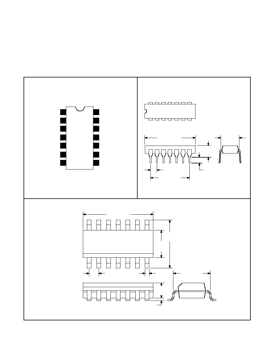
Pin Connection Diagram
NTE978SM
V
CC
Output
Control Voltage
Threshold
Reset
Control Voltage
Trigger
Reset
GND
Discharge
1
2
3
4
Discharge
Threshold
5
Output
6
Trigger
7
14
13
12
11
10
9
8
NTE978, NTE978C
.600 (15.24)
1
7
14
8
.300
(7.62)
.200 (5.08)
Max
.100 (2.45)
.099 (2.5) Min
.785 (19.95)
Max
061
(1.53)
.198 (5.03)
.236
(5.99)
NOTE: Pin1 on Beveled Edge
.154
(3.91)
.006 (.152)
7
8
.340 (8.64)
016
(.406)
1
14
.050 (1.27)