PRELIMINARY PRODUCT SPECIFICATION
Nordic VLSI ASA - Vestre Rosten 81, N-7075 Tiller, Norway - Phone +4772898900 -
Fax +4772898989
Revision: 2.5
February 19th, 2003
Page 1 of 9
10-Bit 1MSPS 0.18
µ
m
Analog-to-Digital Converter IP
FEATURES
∑
1.8V power supply
∑
SNR typ 58dB for (f
in
= 10kHz)
∑
Scaleable low power (2.9mW @
1.8V and 1MSPS)
∑
2.1mW power dissipation with
external bandgap reference
∑
Compact area (0.2mm
2
)
∑
Sampling frequency from 100kHz
to 1MHz
∑
Programmable resolution. 6, 8, 10
and 12 bits
∑
9 multiplexed single ended inputs
∑
Low input capacitance
∑
Three power saving idle modes
APPLICATIONS
∑
Instrumentation
∑
Wireless communication
GENERAL DESCRIPTION
The nAD1001-18 is a compact, high-speed, low power 6 to 12 bit monolithic analog-
to-digital converter, implemented in a 0.18
µ
m generic CMOS process. The converter
includes a sample and hold. Using internal references, the full scale range is 1.2V with
an input signal range of 0 to 1.2V. The full scale range can be set between 0.8V and
1.5V using external references. It operates from a single 1.8V supply. The bias current
level for the ADC can be programmed in 8 steps. Hence, the power dissipation of the
device can be minimised for the current operation frequency. The nAD1001-18 has an
algorithmic architecture - resulting in low silicon area. The core occupies less than
0.2mm
2
of die area in a standard single poly 0.18
µ
m CMOS process. The fully
differential architecture makes it insensitive to substrate noise. Thus it is ideal as a
mixed signal ASIC macro cell.
QUICK REFERENCE DATA
Symbol
Parameter
Conditions
Min.
Typ.
Max.
Unit
V
DD
Supply voltage
1.6
1.8
2.0
V
P
D
Power dissipation
(1 MSPS / 6 MHz clock)
Except digital
output drivers
2.9
mW
DNL
Differential nonlinearity
f
IN
=0.9kHz
±0.5
LSB
INL
Integral nonlinearity
f
IN
=0.9kHz
±
0.75
LSB
SNR
Signal to noise ratio
f
IN
=10kHz
53
58
dB
SFDR
Spurious free dynamic range
f
IN
=10kHz
65
dB
Table 1: Quick reference data
nAD1001-18
PRELIMINARY PRODUCT SPECIFICATION
nAD1001-18: 10 Bit 1 MSPS 0.18
µ
µ
µ
µ
m ADC IP
Nordic VLSI ASA - Vestre Rosten 81, N-7075 Tiller, Norway - Phone +4772898900 -
Fax +4772898989
Revision: 2.5
February 19th, 2003
Page 2 of 9
ELECTRICAL SPECIFICATIONS
(
At T
A
= 25
∞
C, V
DD
= 1.8V, Sampling Rate = 1 MHz (6 MHz clock frequency), Input frequency = 10
kHz, 50% duty cycle clock unless otherwise noted, 1.2V VFS
)
Symbol Parameter (condition)
Test
Level
Min.
Typ.
Max.
Units
DC Accuracy
DNL
Differential Nonlinearity
f
IN
= 0.9991 kHz
III
±
0.5
LSB
INL
Integral Nonlinearity
f
IN
= 0.9991 kHz
III
±
0.75
LSB
V
OS
Midscale offset
±
1
%FS
G
Gain Error
±
1
%FS
Dynamic Performance
SNR
Signal to Noise Ratio (without
harmonics)
f
IN
= 10 kHz
III
53
58
dBFS
Signal to Noise and Distortion Ratio
f
IN
= 10 kHz
III
57
dBFS
SFDR
Spurious Free Dynamic Range
f
IN
= 10 kHz
III
65
dB
Analog Input
V
FSR
Input Voltage Range
III
0.8
1.2
1.5
V
C
INA
Input Capacitance
1.2
pF
Reference Voltages
Internal reference voltage drift
100
ppm/
∞
C
FSR
Full scale range (internal reference)
1.2
V
FSR
Full scale range (external reference)
0.8
1.5
V
V
FS
Reference voltage input (external ref)
III
0.8
1.5
V
Switching Performance
F
S max
Maximum Conversion Rate
III
100
kSPS
F
S min
Minimum Conversion Rate
10
kSPS
t
AP
Aperture delay, IP
V
0.5
ns
t
setup
Setup time CSTARTN
5
ns
t
hold
Hold time CSTARTN
0.1
ns
t
h
Output hold time, IP (0.1 - 0.8 pF load)
V
0.15
ns
t
d
Output delay time, IP (0.1 - 0.8 pF load)
V
1.0
ns
Digital Inputs and Outputs
Logic signals referred to AVDD
III
(table continued on next page)

PRELIMINARY PRODUCT SPECIFICATION
nAD1001-18: 10 Bit 1 MSPS 0.18
µ
µ
µ
µ
m ADC IP
Nordic VLSI ASA - Vestre Rosten 81, N-7075 Tiller, Norway - Phone +4772898900 -
Fax +4772898989
Revision: 2.5
February 19th, 2003
Page 3 of 9
Power Supply
V
DD
Supply voltage
V
1.6
1.8
2.0
V
I
DD
Supply current (except digital output)
III
1.6
mA
V
SS
Supply voltage
GND
P
D
Power dissipation (except digital output)
(active 1 MSPS)
III
2.9
mW
P
D
Power dissipation (except digital output)
(active 1 MSPS). EXTVBG high and
1.2V applied to pin VBG
2.1
mW
P
D
Power dissipation (except digital output)
(active 100 kSPS)
III
1.7
mW
P
D
Power dissipation (except digital output)
Standby Mode
III
1.5
mW
P
D
Power dissipation (except digital output)
Sleep Mode
III
1.2
mW
P
D
Power dissipation (except digital output)
Power Down Mode
III
2
µW
t
start
Start-up time from Power down (With
10nF || 1nF decoupling on CMEXT)
300
µ
s
t
start
Start-up time from Sleep mode
3
clock cycles
t
start
Start-up time from Stand By
2
clock cycles
T
Junction operating temperature
-40
+125
∞
C
Table 2: Electrical specifications
Test Levels
Test Level I: 100% production tested at +25∞C
Test Level II: 100% production tested at +25∞C and sample tested at specified
temperatures
Test Level III: Sample tested only
Test Level IV: Parameter is guaranteed by design and characterization testing
Test Level V: Parameter is typical value only
Test Level VI: 100% production tested at +25∞C. Guaranteed by design and
characterization testing for industrial temperature range
PRELIMINARY PRODUCT SPECIFICATION
nAD1001-18: 10 Bit 1 MSPS 0.18
µ
µ
µ
µ
m ADC IP
Nordic VLSI ASA - Vestre Rosten 81, N-7075 Tiller, Norway - Phone +4772898900 -
Fax +4772898989
Revision: 2.5
February 19th, 2003
Page 4 of 9
ABSOLUTE MAXIMUM RATINGS
Supply voltages
V
DD
...............................- 0.2V to +2.2V
Input voltages
Analog In ........ - 0.2V to AVDD + 0.2V
Digital In......... - 0.2V to AVDD + 0.2V
CLOCK .......... - 0.2V to AVDD + 0.2V
Temperatures
Operating Temperature....-40 to +125
∞
C
Note: Stress above one or more of the limiting values may cause permanent damage
to the device.
PIN FUNCTIONS
Pin Name
Description
IN_SE[8:0]
Input signal pins.
INREF
Input signal ground. Connect to external ground. No current should go through this pin
CHSEL[3:0]
Input signal selector. Selecting inputs 8:0. Binary value corresponds to input signal number.
RESCTRL[1:0]
Control ADC resolution. 00: 6-bits, 01: 8-bits, 10: 10-bits, 11: 12-bits
VFS
Reference input pin. Full scale range of converter from 0V to voltage on VFS pin if VFSSEL is high.
VBG
Bandgap voltage input (1.2V) if EXTVBG is high.
BIASCTRL[2:0]
Bias control pins. (See Modes of operation)
OPM[1:0]
Operating mode control. (See Modes of operation)
DIFFM
Differential mode if high. IN_SE[0] is used as negative input. CHSEL selects the positive input.
Ensure that input common mode level is VDD/2 (+/- 200mV) when running in this mode.
CLK
ADC Clock
CSTARTN
Input signal is sampled when low. Conversion started at first rising clock edge after low to high
transition. Conversions running continuously if kept high.
Note setup and hold times of this pin.
Do not keep CSTARTN low for more than 3 clock periods. Keep high for at least 5 clock periods
after keeping low
EXTVBG
Disables internal bandgap reference when high. Apply 1.21V to pin VBG
VFSSEL
Selects VFS input to set full scale range if high. Input signal range is 0V to 1.2V if low.
DRDY
Data Ready. Kept high for one clock cycle after data become available on BITO
BITO[11:0]
Digital outputs ( MSB to LSB). Data held until new data become available.
RFLAG[2:0]
Out of range flags: RFLAG[0]: Out of Range, RFLAG[1]: Over Range, RFLAG[2]: Under Range
EXTREF
Disables internal voltage reference when high. External voltage must be applied to REF[1:0]
REF[1:0]
Reference signal. Leave open unless EXTREF is set high. Decouple with 1nF capacitors to ground for
optimum performance.
CMEXT
Reference signal. Decouple with 1nF in parallel with 10nF capacitor to ground for optimum
performance.
AVDD
Power
AVSS
Ground
Table 3: Pin functions
PRELIMINARY PRODUCT SPECIFICATION
nAD1001-18: 10 Bit 1 MSPS 0.18
µ
µ
µ
µ
m ADC IP
Nordic VLSI ASA - Vestre Rosten 81, N-7075 Tiller, Norway - Phone +4772898900 -
Fax +4772898989
Revision: 2.5
February 19th, 2003
Page 5 of 9
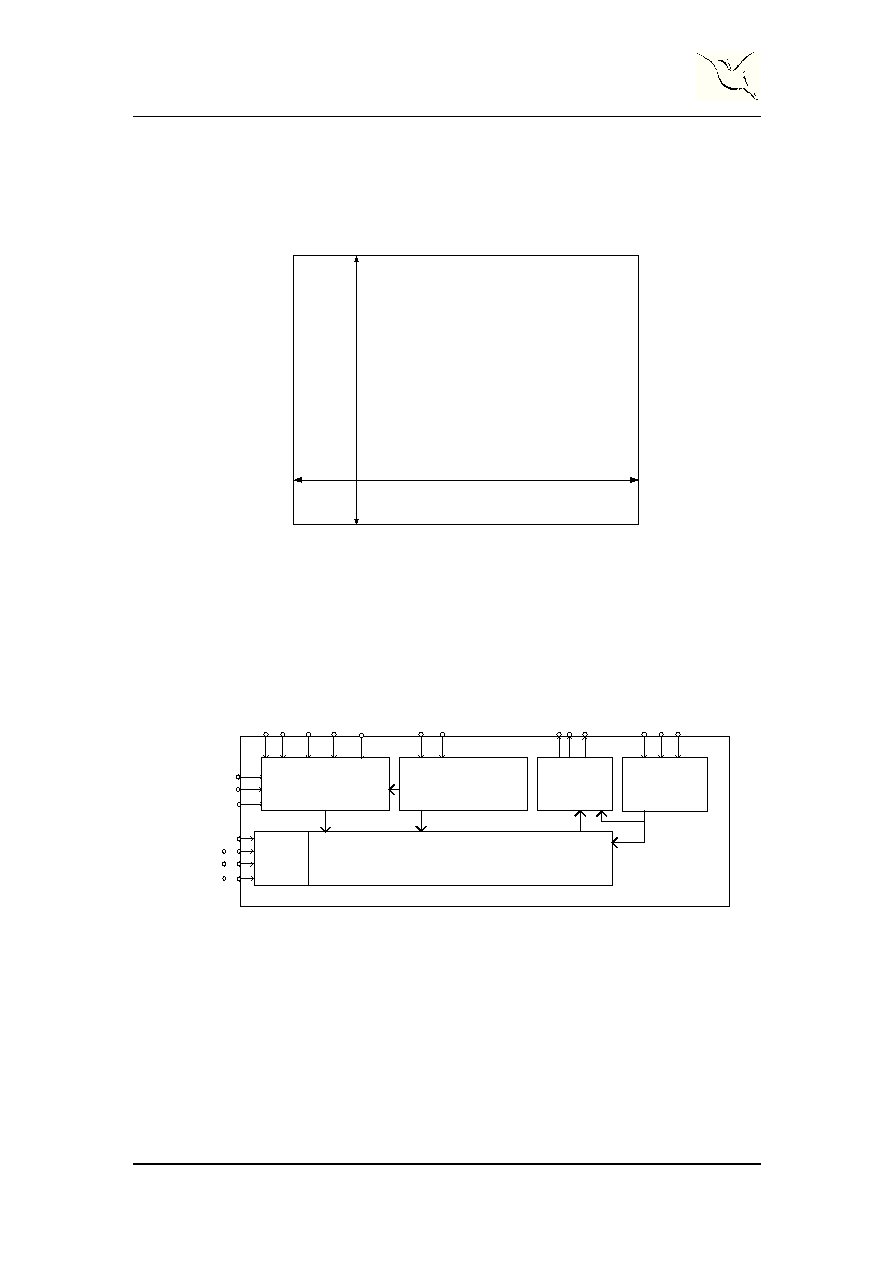
IP BLOCK LAYOUT
nAD1001-18
REF[1:0]
VFS
I
N
_S
E[
8
:
0]
BIASCTRL[2:0]
AVSS
AVDD
CMEXT
INREF
Y
=
400um
VFSSEL
OPM[1:0]
VBG
DRDY
EXTREF
EXTVBG
X=512.8um
RFLAG[2:0]
BITO[11:0]
CLK
DIFFM
CHSEL[3:0]
RESCTRL[1:0]
CSTARTN
Figure 1: Size and pin placement for nAD1001-18 IP. X = 512.8
µ
m Y = 400
µ
m
FUNCTIONAL BLOCK DIAGRAM
CURRENT
BIAS
VOLTAGE
REFERENCE
DIGITAL
CLOCK
DRIVER
CONVERTER CORE
INREF
EX
TREF
BI
A
S
CTRL[
2
:0]
O
P
M[
1:0]
CLK
BI
T
O
[
11:0]
RF
L
A
G
[
2:0]
MUX
CHSEL[3:0]
VFS
VB
G
RESCTRL[
1
:
0
]
CS
TA
RTN
DR
DY
DIFFM
CMEXT
REF[1:0]
CMINT
EX
TV
BG
VFSSEL
IN_SE[8:0]
Figure 2: Functional Block diagram nAD1001-18