
PRELIMINARY PRODUCT SPECIFICATION
Main office: Nordic VLSI ASA - Vestre Rosten 81, N-7075 Tiller, Norway - Phone +4772898900 - Fax +4772898989
Revision: 2.0
Page 1 of 9
November 28th, 2002
10-Bit 100kSPS 0.18
µ
m
Analog-to-Digital Converter IP
FEATURES
∑
1.8V power supply
∑
SNR typ 58dB for (f
in
= 10kHz)
∑
Low power (630
µ
W @ 1.8V and
100kSPS)
∑
Compact area (<0.2mm
2
)
∑
Sampling frequency from 10kHz to
100kHz
∑
Programmable resolution. 6, 8, 10
and 12 bits
∑
9 multiplexed single ended inputs
∑
Low input capacitance
∑
Three power saving idle modes
APPLICATIONS
∑
Instrumentation
GENERAL DESCRIPTION
The nAD10100K-18 is a compact, high-speed, low power 6 to 12 bit monolithic
analog-to-digital converter, implemented in a 0.18
µ
m single poly CMOS process with
MiM capacitor option. The converter includes a sample and hold. Using internal
references, the full scale range is 1.2V with an input signal range of 0 to 1.2V. The
full scale range can be set between 0.75V and 1.5V using external references. It
operates from a single 1.8V supply. The bias current level for the ADC can be
programmed in 8 steps. Hence, the power dissipation of the device can be minimised
for the current operation frequency.
The nAD10100K-18 has an algorithmic architecture - resulting in low silicon area.
The core occupies less than 0.2mm
2
of die area in a standard single poly 0.18
µ
m
CMOS process with MiM capacitor option. The fully differential architecture makes it
insensitive to substrate noise. Thus it is ideal as a mixed signal ASIC macro cell.
QUICK REFERENCE DATA
Symbol
Parameter
Conditions
Min.
Typ.
Max.
Unit
V
DD
Supply voltage
1.55
1.8
2.0
V
P
D
Power dissipation
(100 kSPS)
Except digital
output drivers
630
µ
W
DNL
Differential nonlinearity
f
IN
=0.9kHz
±0.5
LSB
INL
Integral nonlinearity
f
IN
=0.9kHz
±
0.75
LSB
SNR
Signal to noise ratio
f
IN
=10kHz
53
58
dB
SFDR
Spurious free dynamic
range
f
IN
=10kHz
65
dB
Table 1: Quick reference data
nAD10100K-18
PRELIMINARY PRODUCT SPECIFICATION
nAD10100K-18: 10 Bit 100 kSPS 0.18
µ
µ
µ
µ
m ADC IP
Main office: Nordic VLSI ASA - Vestre Rosten 81, N-7075 Tiller, Norway - Phone +4772898900 - Fax +4772898989
Revision: 2.0
Page 2 of 9
November 28th, 2002
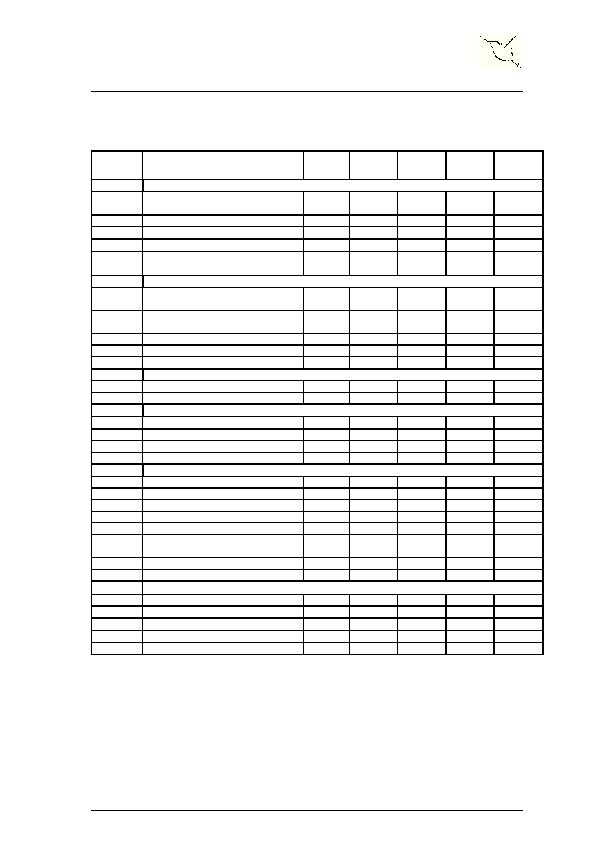
ELECTRICAL SPECIFICATIONS
(
At T
A
= 25
∞
C, V
DD
= 1.8V, Sampling Rate = 100kHz, Input frequency = 10kHz, 50% duty cycle clock
and 300nF Reference decoupling unless otherwise noted
)
Symbol Parameter (condition)
Test
Level
Min.
Typ.
Max.
Units
DC Accuracy
DNL
Differential Nonlinearity
f
IN
= 0.9991 kHz
III
±
0.5
LSB
INL
Integral Nonlinearity
f
IN
= 0.9991 kHz
III
±
0.75
LSB
V
OS
Midscale offset
±
1
%FS
CMRR
Common Mode Rejection Ratio
-59
dB
G
Gain Error
±
1
%FS
Dynamic Performance
SNR
Signal to Noise Ratio (without
harmonics)
f
IN
= 10 kHz
III
53
58
dBFS
SINAD
Signal to Noise and Distortion Ratio
f
IN
= 10 MHz
III
57
dBFS
SFDR
Spurious Free Dynamic Range
f
IN
= 10 kHz
III
65
dB
Analog Input
V
FSR
Input Voltage Range
III
1.5
V
C
INA
Input Capacitance
1.5
pF
Reference Voltages
Internal reference voltage drift
100
ppm/
∞
C
FSR
Full scale range (internal reference)
1.2
V
FSR
Full scale range (external reference)
0.8
1.5
V
V
FS
Reference voltage input (external ref)
III
0.8
1.5
V
Switching Performance
F
S max
Maximum Conversion Rate
III
100
kSPS
F
S min
Minimum Conversion Rate
10
kSPS
d
p
Pipeline delay
IV
TBD
t
AP
Aperture delay, IP
V
TBD
ns
t
setup
Setup time CSTARTN
5
ns
t
hold
Hold time CSTARTN
0.1
ns
t
h
Output hold time, IP (0.1 - 0.8 pF load)
V
0.15
ns
t
d
Output delay time, IP (0.1 - 0.8 pF load)
V
1.0
ns
t
AP
Aperture delay, with bonding pad
V
TBD
ns
Digital Inputs
V
IL
Logic "0" voltage
III
0.4
V
V
IH
Logic "1" voltage
III
V
DD
≠0.4
V
I
IL
Logic "0" current (V
I
=V
SS
)
III
±
10
µ
A
I
IH
Logic "1" current (V
I
=V
DD
)
III
±
10
µ
A
C
IND
Input Capacitance
III
0.03
0.1
pF
(table continued on next page)

PRELIMINARY PRODUCT SPECIFICATION
nAD10100K-18: 10 Bit 100 kSPS 0.18
µ
µ
µ
µ
m ADC IP
Main office: Nordic VLSI ASA - Vestre Rosten 81, N-7075 Tiller, Norway - Phone +4772898900 - Fax +4772898989
Revision: 2.0
Page 3 of 9
November 28th, 2002
Digital Outputs
V
OL
Logic "0" voltage (I = 2 mA)
III
0.2
0.4
V
V
OH
Logic "1" voltage (I = 2 mA)
III
85% V
DD
90% V
DD
V
Power Supply
V
DD
Supply voltage
V
1.6
1.8
2.0
V
I
DD
Supply current (except digital output)
III
277
µ
A
V
SS
Supply voltage
GND
P
D
Power dissipation (except digital output)
(active 100 kSPS)
III
630
µ
W
P
D
Power dissipation (except digital output)
(active 10 kSPS)
III
TBD
mW
P
D
Power dissipation (except digital output)
Power Down Mode
III
TBD
µW
P
D
Power dissipation (except digital output)
Sleep Mode
III
TBD
mW
P
D
Power dissipation (except digital output)
Standby Mode
III
TBD
mW
t
start
Start-up time from Power down
TBD
ms
t
start
Start-up time from Sleep mode
TBD
µ
s
t
start
Start-up time from Stand By
TBD
clock cycles
T
Junction operating temperature
-40
+125
∞
C
Table 2: Electrical specifications
Test Levels
Test Level I: 100% production tested at +25∞C
Test Level II: 100% production tested at +25∞C and sample tested at specified
temperatures
Test Level III: Sample tested only
Test Level IV: Parameter is guaranteed by design and characterization testing
Test Level V: Parameter is typical value only
Test Level VI: 100% production tested at +25∞C. Guaranteed by design and
characterization testing for industrial temperature range
ABSOLUTE MAXIMUM RATINGS
Supply voltages
V
DD
...............................- 0.2V to +2.2V
OV
DD
..............................- 0.2V to 3.6V
Input voltages
Analog In .............- 0.2V to V
DD
+ 0.2V
Digital In.........................- 0.2V to 3.6V
REF
P
....................- 0.2V to V
DD
+ 0.2V
REF
N
....................- 0.2V to V
DD
+ 0.2V
CLOCK ..........................- 0.2V to 3.6V
Temperatures
Operating Temperature....-40 to +125
∞
C
Storage Temperature.. - 65 to +125
∞
C
Note: Stress above one or more of the limiting values may cause permanent damage
to the device.

PRELIMINARY PRODUCT SPECIFICATION
nAD10100K-18: 10 Bit 100 kSPS 0.18
µ
µ
µ
µ
m ADC IP
Main office: Nordic VLSI ASA - Vestre Rosten 81, N-7075 Tiller, Norway - Phone +4772898900 - Fax +4772898989
Revision: 2.0
Page 4 of 9
November 28th, 2002
PIN FUNCTIONS
Pin Name
Description
IN_SE[8:0]
Input signal pins. Input signal range from 0 to V
FS
of V
BG
dependig on state of EXTREF
INREF
Input signal ground. Connect to external groud. No current should go through this pin
CHSEL[3:0]
Input signal selector. Selecting inputs 8:0. Binary value corresponds to input signal number.
RESCTRL[1:0]
Control ADC resolution. 00: 6-bits, 01: 8-bits, 10: 10-bits, 11: 12-bits
VFS
Reference input pin.
VBG
Bandgap voltage input (1.21V)
BIASCTRL[2:0],
NPD, SLEEP,
STBY
Operating mode and bias control pins. (See Modes of operation)
DIFFM
Differential mode. IN_SE[0] is used as negative input. CHSEL selects the positive input. Ensure that
input common mode level is VDD/2 (+/- 200mV) when running in this mode.
CLK
ADC Clock
CSTARTN
Input signal is sampled when low. Conversion started at first rising clock edge after low to high
transition. Conversions running continuously if kept high.
Avoid toggling this pin exactly at a rising edge of the clock to reduce risk of metastability
DRDY
Data Ready. Kept high for one clock cycle after data are made available on BITO
BITO[11:0]
Digital outputs ( MSB to LSB). Data held until new data are made available.
RFLAG[2:0]
Out of range flags: RFLAG[0]: Out of Range, RFLAG[1]: Over Range, RFLAG[2]: Under Range
EXTREF
Disables internal voltage reference when high. External voltage must be applied to REF[1:0]
REF_SE[1:0]
Reference signal. Leave open
REF[1:0]
Reference signal. Leave open unless EXTREF is set high.
CMINT, CMEXT
Reference signals. Leave open.
VDD
Digital power
AVDD
Analog power
AVSS
Analog and digital ground
Table 3: Pin functions
IP BLOCK LAYOUT
TBD
Figure 1: Size and pin placement for nAD10100K-18 IP
FUNCTIONAL BLOCK DIAGRAM
CURRENT
BIAS
VOLTAGE
REFERENCE
DIGITAL
CLOCK
DRIVER
CONVERTER CORE
INREF
IN_SE[8:0]
EX
TREF
BI
A
S
CTRL[
2
:0]
SLEEP
NPD
CLO
C
K
BI
T
O
[
11:0]
RF
L
A
G
[
2:0]
MUX
CHSEL[3:0]
VFS
VB
G
STB
Y
RESCTRL[
1
:
0
]
CS
TA
RTN
DR
DY
DIFFM
CMEXT
REF_SE[1:0]
REF[1:0]
CMINT
Figure 2: Functional Block diagram nAD10100K-18

PRELIMINARY PRODUCT SPECIFICATION
nAD10100K-18: 10 Bit 100 kSPS 0.18
µ
µ
µ
µ
m ADC IP
Main office: Nordic VLSI ASA - Vestre Rosten 81, N-7075 Tiller, Norway - Phone +4772898900 - Fax +4772898989
Revision: 2.0
Page 5 of 9
November 28th, 2002
MODES OF OPERATION
The ADC has four different modes of operation, controlled as described in Table 4:
Digital control
Mode of operation
STBY
SLEEP
NPD
CLOCK
Active
LOW
LOW
HIGH
RUNNING
Standby
HIGH
LOW
HIGH
STOPPED
Sleep
HIGH
HIGH
HIGH
STOPPED
Power down
X
X
LOW
STOPPED
Table 4: Control settings for ADC operational modes
Active mode
In the active mode, the ADC is fully functional.
A performance versus power consumption trade off can be made by adding or
subtracting 12.5% of the pipeline bias current with the bias1 and bias0 pins:
BIASCTRL[2:0]
Clock rate
0
0
0
500kHz
0
0
1
1000kHz
Only available for differential mode
0
1
0
1500kHz Only available for differential mode
0
1
1
2000kHz Only available for differential mode
1
0
0
2500kHz Only available for differential mode
1
0
1
3000kHz Only available for differential mode
1
1
0
4000kHz Only available for differential mode
1
1
1
5000kHz Only available for differential mode
Idle modes
In the three idle modes, the ADC is not functional. The different modes are
distinguished primary by power consumption and start-up time. Start-up time is
defined as the time it takes for the ADC to reach full performance in active mode
when switched from an idle mode. Refer to `Electrical Specifications' for power
consumption and start-up times for the different modes.

PRELIMINARY PRODUCT SPECIFICATION
nAD10100K-18: 10 Bit 100 kSPS 0.18
µ
µ
µ
µ
m ADC IP
Main office: Nordic VLSI ASA - Vestre Rosten 81, N-7075 Tiller, Norway - Phone +4772898900 - Fax +4772898989
Revision: 2.0
Page 6 of 9
November 28th, 2002
TIMING DIAGRAM
CLK
CSTARTN
Analog
Input
Start
Conversion
DRDY
BITO[11:0]
d
p
t
AP
Start
sampling
TBD
Figure 3: Timing diagram
(Not updated)
Cycle time:
The cycle time is the time between each sampling of the input signal in case the ADC is run
continuously keeping the CSTARTN signal high all the time. This time will vary depending on the
resolution. This delay is: N/2+1 clock cycles where N is the number of bits
Conversion time (d
p
):
The conversion time is the time from a rising edge on CSTARTN to a rising edge on DRDY.
This time is: N/2+3
INPUT SIGNAL RANGE
The input signal range is determined by the voltage on the VFS pin and the DIFFM
signal.
DIFFM=0
The range for the input signal (IN_SE[x]) is 0 to v(VFS)
DIFFM=1
The range for the input signal (IN_SE[x] - IN_SE[0]) is +/-v(VFS)/2

PRELIMINARY PRODUCT SPECIFICATION
nAD10100K-18: 10 Bit 100 kSPS 0.18
µ
µ
µ
µ
m ADC IP
Main office: Nordic VLSI ASA - Vestre Rosten 81, N-7075 Tiller, Norway - Phone +4772898900 - Fax +4772898989
Revision: 2.0
Page 7 of 9
November 28th, 2002
DEFINITIONS
Data sheet status
Objective product specification
This datasheet contains target specifications for product development.
Preliminary product
specification
This datasheet contains preliminary data; supplementary data may be
published from Nordic VLSI ASA later.
Product specification
This datasheet contains final product specifications.
Limiting values
Stress above one or more of the limiting values may cause permanent damage to the device. These are stress
ratings only and operation of the device at these or at any other conditions above those given in the
Specifications sections of the specification is not implied. Exposure to limiting values for extended periods may
affect device reliability.
Application information
Where application information is given, it is advisory and does not form part of the specification.
Table 5: Definitions
LIFE SUPPORT APPLICATIONS
These products are not designed for use in life support appliances, devices, or systems
where malfunction of these products can reasonably be expected to result in personal
injury. Nordic VLSI ASA customers using or selling these products for use in such
applications do so at their own risk and agree fully indemnify Nordic VLSI ASA for
any damages resulting from such improper use or sale.

PRELIMINARY PRODUCT SPECIFICATION
nAD10100K-18: 10 Bit 100 kSPS 0.18
µ
µ
µ
µ
m ADC IP
Main office: Nordic VLSI ASA - Vestre Rosten 81, N-7075 Tiller, Norway - Phone +4772898900 - Fax +4772898989
Revision: 2.0
Page 8 of 9
November 28th, 2002
APPLICATION INFORMATION
TBD

PRELIMINARY PRODUCT SPECIFICATION
nAD10100K-18: 10 Bit 100 kSPS 0.18
µ
µ
µ
µ
m ADC IP
Main office: Nordic VLSI ASA - Vestre Rosten 81, N-7075 Tiller, Norway - Phone +4772898900 - Fax +4772898989
Revision: 2.0
Page 9 of 9
November 28th, 2002
DESIGN CENTER
Nordic VLSI ASA
Vestre Rosten 81
N-7075 TILLER
NORWAY
Telephone:
+47 72898900
Telefax:
+47 72898989
E-mail: For further information regarding our state of the art data converters, please e-
mail us at datacon@nvlsi.no.
World Wide Web/Internet: Visit our site at http://www.nvlsi.no.
ORDERING INFORMATION
Type number
Description
Price
nAD10100K-18-IC
nAD10100K-18 sample in SSOP28 package
(limited availability)
USD 50
nAD10100K-18-EVB
nAD10100K-18 evaluation board including
characterisation report and user guide
USD 300
Table 6: Ordering information
Objective Product Specification. Revision Date: November 28
th
, 2002
All rights reserved Æ. Reproduction in whole or in part is prohibited without the prior
written permission of the copyright holder. Company and product names referred to in
this datasheet belong to their respective copyright/trademark holders.