PRELIMINARY PRODUCT SPECIFICATION
nAD10110x2-18a
Dual 10-bit 110 MSPS Analog-to-Digital Converter IP
Nordic VLSI ASA - Vestre Rosten 81, N-7075 Tiller, Norway - Phone +4772898900 - Fax +4772898989
Revision: 1.0B
Page 1 of 13
2003-04-10
FEATURES
∑ Dual 10-bit ADC
∑ Up to 110 MSPS Conversion Rate
∑ Single 1.8 V Power Supply
∑ 1.5 V p-p Differential Inputs
∑ Excellent Dynamic Performance
59 dBFS SNR at Fin = 10 MHz
70 dBc SFDR at Fin = 10 MHz
∑ 600 MHz Analog Input Bandwidth
∑ Low Power Consumption
160mW at 110 MSPS
40 mW at 25 MSPS
∑ Excellent Gain and Phase Matching
∑ Dynamic Power Scaling
∑ Power Saving Idle Modes
∑ Internal Voltage Reference
∑ 1.6 mm
2
Core Area
APPLICATIONS
∑ Communication Receive Channel
WLAN / HiperLan / 802.11x
∑ Quadrature ( I and Q ) Modulation
∑ Digital Imaging / Video
∑ TV / Video / Radio Decoders
∑ Graphic Capture
GENERAL DESCRIPTION
The nAD10110x2-18a is a monolithic, high-speed,
low power, dual channel analog-to-digital
converter silicon IP. It uses a fully differential
multistage pipeline architecture with digital error
correction to provide 10-bit accuracy from 15 to
110 MSPS conversion speed. The core includes a
wide-band sample-and-hold and an internal voltage
reference that provides a nominal full-scale range
of 1.5 V peak-to-peak. The ADC is designed for
high dynamic performance at input frequencies up
to Nyquist and beyond. It thus represents an ideal
solution for
demanding applications like broadband
communication, digital imaging and multimedia.
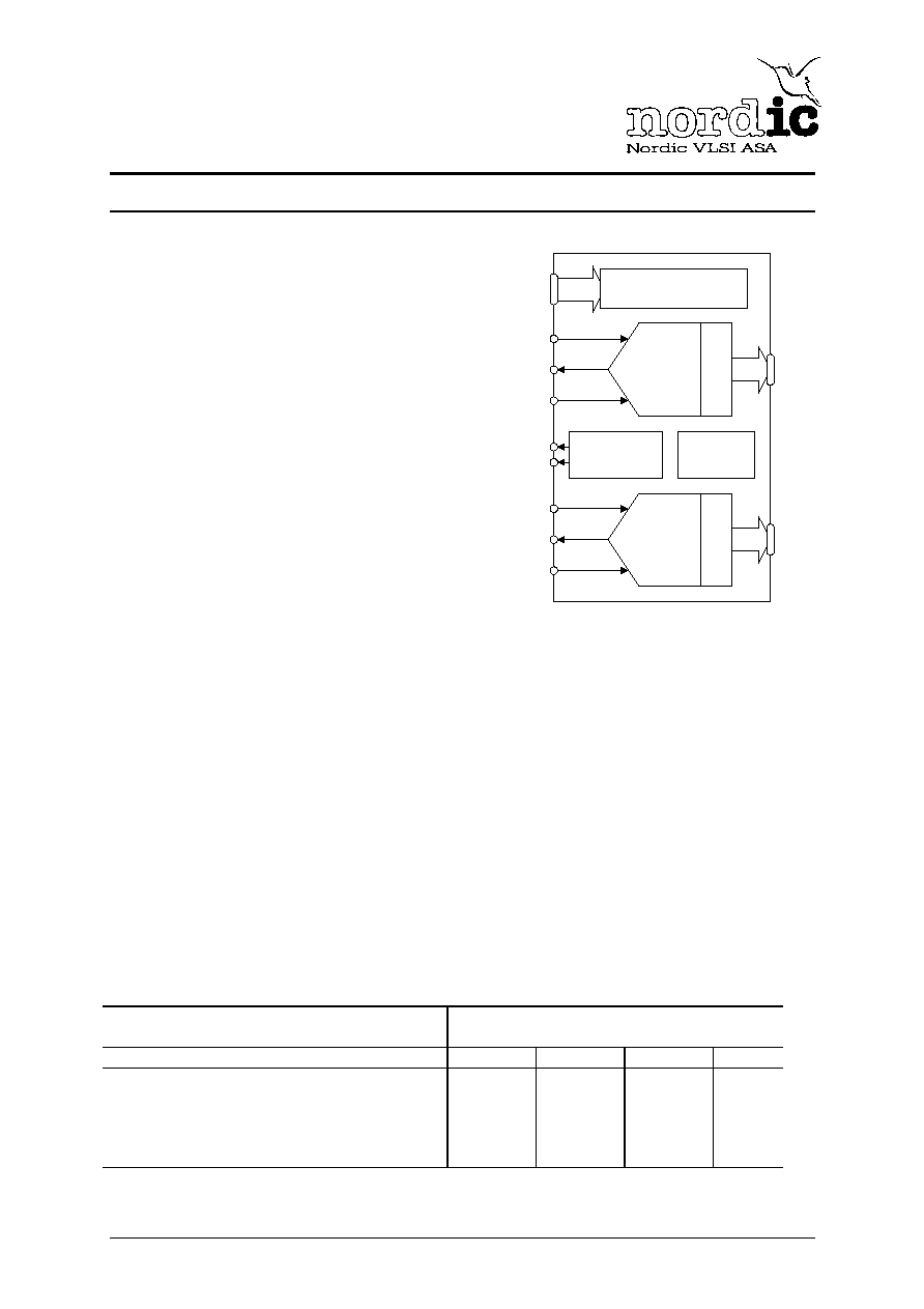
PIPELINE
ADC
DIG
I
T
A
L
CORRE
CTI
O
N
DYNAMIC
BIAS
VOLTAGE
REFERENCE
BITO0[9:0]
RFLAG0[2:0]
OPM[1:0]
CLK
EXTREF
TIMING GENERATOR
DIGITAL CONTROL
INP0
VCM0
INN0
REFP
REFN
PIPELINE
ADC
DI
GIT
A
L
CORRECT
I
O
N
BITO1[9:0]
RFLAG1[2:0]
INP1
VCM1
INN1
Figure 1. Functional block diagram
The ADC consumes only 160 mW at 110 MSPS
operation. Dynamic power scaling means that the
power consumption is scaled with the operating
frequency resulting in only 40 mW consumption at
25 MSPS operation. Combined with power saving
idle modes the ADC is suitable for battery powered
devices. Output data is available in a binary offset
coded format. Three out-of-range indicator bits are
also available for determining if the input signal is
over-range, under-range or out-of-range.
Implemented in a generic 0.18
µm CMOS process,
operating from a single 1.8 V supply and
employing a fully differential architecture it
represents an ideal ADC for highly integrated
mixed-signal systems.
QUICK REFERENCE DATA
IP Type / Technology
Hard Macro / TSMC Generic, 6 Metal 0.18
µm CMOS
IP Area / Dimensions
1.6 mm
2
/ 1.180
◊ 1.32 mm
Parameter
Min.
Typ.
Max.
Unit
Supply Voltage
1.6
1.8
2.0
V
Power Dissipation, @ F
CLK
= 110 MHz
160
mW
Differential Non Linearity
± 0.3
± 0.5
LSB
Integral Non Linearity
± 0.4
± 1.0
LSB
Signal-to-Noise Ration, F
IN
= 10 MHz
59
dBFS
Spurious-Free-Dynamic Range, F
IN
= 10 MHz
70
dBc
Table 1. nAD10110x2-18a quick reference data

PRELIMINARY PRODUCT SPECIFICATION
nAD10110x2-18a - Dual 10-bit 110 MSPS Analog-to-Digital Converter IP
Nordic VLSI
Page 2 of 13
Revision: 1.0B
ELECTRICAL SPECIFICATIONS
DC SPECIFICATIONS
( At T
A
= 25 ∫C, V
AVDD
= V
VDD
= 1.8 V, F
CLK
= 110 MHz, F
IN
= 10 MHz, internal references, differential full-
scale input signal, 50 % duty cycle clock, and 10nF reference decoupling, data per channel, unless otherwise
noted )
Symbol
Parameter (condition)
Test
level
Min.
Typ.
Max.
Unit
DC ACCURACY
N
Resolution
10
Bits
NMC
No Missing Codes Guaranteed
10
Bits
INL
Integral Non Linearity
± 0.4
± 1.0
LSB
DNL
Differential Non Linearity
± 0.3
± 0.5
LSB
G
Gain Error
± 1.0
% FSR
Gain Matching between channel 0 and 1
0.5
% FSR
V
OS
Offset Error
± 1.0
% FSR
ANALOG INPUT
V
FSR
Input Differential Voltage Range
± 0.75
V
V
VCM,EXT
Input Common Mode Voltage
0.8
0.9
1.0
V
Input Impedance
1.5
pF
AIBW
Analog Input Bandwidth
600
MHz
REFERENCE VOLTAGES
V
REFP
Internal Positive Voltage Reference
1.275
V
V
REFN
Internal Negative Voltage Reference
0.525
V
V
RR
Internal Reference Range
0.75
V
FSR
Internal Differential Full-scale Range
1.5
V p-p
V
VCM
Internal Reference Common Mode Voltage
0.9
V
Internal Voltage Reference Drift
100
ppm /
∞C
V
RR,EXT
External Reference Range
0.5
0.75
V
FSR
EXT
External Differential Full Scale Range
1
1.5
V p-p
V
RCM,EXT
External Reference Common Mode Voltage
0.8
0.9
1.0
V
POWER SUPPLY
V
AVDD
Positive Analog Supply Voltage
1.6
1.8
2.0
V
V
VDD
Positive Digital Supply Voltage
1.6
1.8
2.0
V
V
SS
Negative Supply Voltage
GND
I
DD
Supply Current, Active
1
110 MSPS
88
mA
I
DD
Supply Current, Active
1
80 MSPS
60
mA
I
DD
Supply Current, Active
1
25 MSPS
22
mA
Supply Current, Standby
2.2
mA
Supply Current, Sleep
1.7
mA
Supply Current, Power down
2.2
µA
P
DD
Power Dissipation, Active
1
110 MSPS
160
mW
P
DD
Power Dissipation, Active
1
80 MSPS
108
mW
P
DD
Power Dissipation, Active
1
25 MSPS
40
mW
Power Dissipation, Standby
4
mW
Power Dissipation, Sleep
3
mW
Power Dissipation, Power down
4
µW
OPERATING CONDITIONS
T
A
Junction Operating Temperature
-40
125
∞C
Table 2. nAD10110x2-18a DC Specifications
1
Both channels active

PRELIMINARY PRODUCT SPECIFICATION
nAD10110x2-18a - Dual 10-bit 110 MSPS Analog-to-Digital Converter IP
Nordic VLSI
Page 3 of 13
Revision: 1.0B
DYNAMIC SPECIFICATIONS
( At T
A
= 25 ∫C, V
AVDD
= V
VDD
= 1.8 V, F
CLK
= 110 MHz, F
IN
= 10 MHz, internal references, differential full-
scale input signal, 50 % duty cycle clock, and 10nF reference decoupling, data per channel, unless otherwise
noted)
Symbol
Parameter (condition)
Test
level
Min.
Typ.
Max.
Unit
SWITCHING PERFORMANCE
F
CLK,MAX
Maximum Conversion Rate
110
MSPS
F
CLK,MIN
Minimum Conversion Rante
15
MSPS
Input Clock Duty Cycle
45
50
55
%
t
pd
Pipeline Delay ( Latency )
5
clocks
t
d
Output Data Delay Time
2
ns
t
h
Output Data Hold Time
1
ns
t
ad
Aperture Delay Time
0.9
ns
t
jitter
Aperture Uncertainty ( Jitter )
1.5
ps rms
t
standby
Start-up Time from Standby Mode
5
clocks
t
sleep
Start-up Time from Sleep Mode
0.5
µs
t
power down
Start-up Time from Power Down Mode
5
µs
t
out-of-range
Out-of-Range Recovery Time
SNR
SIGNAL-TO-NOISE RATIO
110 MSPS, F
IN
= 10 MHz
59
dBFS
110 MSPS, F
IN
= 40 MHz
58.5
dBFS
110 MSPS, F
IN
= 72 MHz
58
dBFS
SINAD
SIGNAL-TO-NOISE-AND DISTORTION
RATIO
110 MSPS, F
IN
= 10 MHz
58
dBFS
110 MSPS, F
IN
= 40 MHz
53
dBFS
110 MSPS, F
IN
= 72 MHz
50
dBFS
SFDR
SPURIOUS FREE DYNAMIC RANGE
110 MSPS, F
IN
= 10 MHz
70
dBc
110 MSPS, F
IN
= 40 MHz
62
dBc
110 MSPS, F
IN
= 72 MHz
52
ENOB
EFFECTIVE NUMBER OF BITS
110 MSPS, F
IN
= 5 MHz
9.6
Bit
110 MSPS, F
IN
= 10 MHz
9.34
Bit
110 MSPS, F
IN
= 40 MHz
8.5
Bit
110 MSPS, F
IN
= 72 MHz
8.0
Bit
CHANNEL ISOLATION
110 MSPS, F
IN
= 5 MHz
50
dBc
Table 3. nAD10110x2-18a Dynamic Specifications

PRELIMINARY PRODUCT SPECIFICATION
nAD10110x2-18a - Dual 10-bit 110 MSPS Analog-to-Digital Converter IP
Nordic VLSI
Page 4 of 13
Revision: 1.0B
DEFINITIONS OF SPECIFICATIONS
Integral Non Linearity ( INL )
The deviation of the ADC transfer function from
the ideal transfer function. The ideal transfer
function is defined as a straight line between the
end points of the transfer characteristic corrected
for gain and offset. INL for each code is calculated
at the code transitions.
Differential Non Linearity ( DNL )
In an ideal ADC every code transition to its
neighbours equals to 1 LSB. DNL is the deviation
of each code transition from the ideal value.
Gain Error
The deviation of the actual difference between the
first and last code transition and the ideal
difference.
Channel Gain Matching
Gain difference between the two channels.
Offset Error
Mid code ideally occurs for zero differential input.
The offset error is the differential input voltage that
gives mid code.
Analog Input Bandwidth
The analog input frequency for which the measured
input signal power has dropped by 3 dB.
Temperature Drift
The temperature drift specifies the maximum
change from the nominal junction temperature to
the minimum and maximum junction temperature.
Maximum Conversion Rate
The maximum conversion rate is the conversion
rate at which electrical specifications are tested.
Minimum Conversion Rate
The minimum conversion rate is the slowest
conversion rate where the ADC is functional.
Pipeline Delay ( Latency )
The pipeline delay is the time it takes from a
sample is taken at the input to the sample is
converted and put on the digital output.
Output Data Delay Time
Output data delay time is the time from the clock
edge that defines valid output data to all data
outputs have reached valid logical levels for the
next data sample.
Output Data Hold Time
Output data hold time is the time from the clock
edge that defines valid output data to the output
data is no longer valid.
Aperture Delay Time
The delay between the sampling clock edge and the
time when the input signal is held for conversion.
Aperture Uncertainty ( Jitter )
Aperture uncertainty or jitter is the variation of the
aperture delay time for successive samples.
Clock Duty Cycle
The fraction of the time the clock spends above the
logic threshold.
Start-up Time from Idle Mode
The time it takes to reach full performance after a
transition from an idle mode to active mode.
Out of Range Recovery Time
The time required for the ADC to return to
specified characteristics after an out-of-range
sample.
Signal-to-Noise Ratio ( SNR )
SNR is the rms ratio of the measured input signal
to the sum of all other spectral components
excluding the dc and the first eight harmonics.
Spurious-Free Dynamic Range ( SFDR )
SFDR is the amplitude difference between the
measured input signal and the highest harmonic
component.
Signal-to-Noise and Distortion Ratio ( SNDR )
SNDR is the rms ratio of the measured input signal
to the sum of all other spectral harmonics
excluding the dc component.
Effective Number of Bits ( ENOB )
Effective number of bits specifies the total rms
noise in terms of bits of resolution the ADC
effectively performs. Generally ENOB depends on
the amplitude and frequency of the input signal
used to test it. The ENOB can be calculated
directly from the SNDR as follows:
6.02
1.76
SNDR
ENOB
-
=
Channel Isolation
Coupling into one channel with a ≠40 dBFS input
signal from the other channel driven by a full-scale
input signal.

PRELIMINARY PRODUCT SPECIFICATION
nAD10110x2-18a - Dual 10-bit 110 MSPS Analog-to-Digital Converter IP
Nordic VLSI
Page 5 of 13
Revision: 1.0B
ABSOLUTE MAXIMUM RATINGS
1
Pin / Condition
Min
Max
Unit
All pins referred to AVSS pin
-0.2
2.2
V
Operating Junction Temperature
-40
125
∞C
Storage Temperature
-65
125
∞C
Table 4. Absolute maximum ratings
EXPLANATION OF TEST LEVELS
Test Level I:
100% production tested at +25∞C
Test Level II:
100% production tested at +25∞C and sample tested at specified temperatures
Test Level III:
Sample tested only
Test Level IV:
Parameter is guaranteed by design and characterization testing
Test Level V:
Parameter is typical value only
Test Level VI:
100% production tested at +25∞C. Guaranteed by design and characterization testing for
industrial temperature range
COMPLETE PINOUT LIST
Name
Type
1)
Description
INP0, INN0
AI
Differential Voltage Inputs, Channel 0
INP1, INN1
AI
Differential Voltage Inputs, Channel 1
VCM0
AO
Common Mode Voltage Output, Channel 0
VCM1
AO
Common Mode Voltage Output, Channel 1
REFP, REFN
AB
Differential Voltage References
CLKA
DI
Conversion Clock A
CLKB
DI
Conversion Clock B
CLKBSEL
DI
Conversion Clock B Select.
CLK_OUT
DO
Reference Clock Output
BITO0[9:0]
DO
Digital Output Code, Channel 0. BITO0[9] is MSB, BITO0[0] is LSB
BITO1[9:0]
DO
Digital Output Code, Channel 1. BITO1[9] is MSB, BITO1[0] is LSB
RFLAG0[2:0]
DO
Digital Over-Range Indicator Output Code, Channel 0
RFLAG1[2:0]
DO
Digital Over-Range Indicator Output Code, Channel 1
OPM[1:0]
DI
Operational Mode Control Input Code
EXTREF
DI
External Reference Control Input Bit
AVDD0
AP
Positive 1.8 V Supply, Channel 0
AVDD1
AP
Positive 1.8 V Supply, Channel 1
AVSS
AG
Ground
1) D = Digital, A = Analog, I = In, O = Out, B = Bidirectional, T = Tristate, P = Power, G = Ground.
Table 5. nAD10110x2-18a pinout list
1
Stress above one or more of the limiting values may cause permanent damage to the device
PRELIMINARY PRODUCT SPECIFICATION
nAD10110x2-18a - Dual 10-bit 110 MSPS Analog-to-Digital Converter IP
Nordic VLSI
Page 6 of 13
Revision: 1.0B
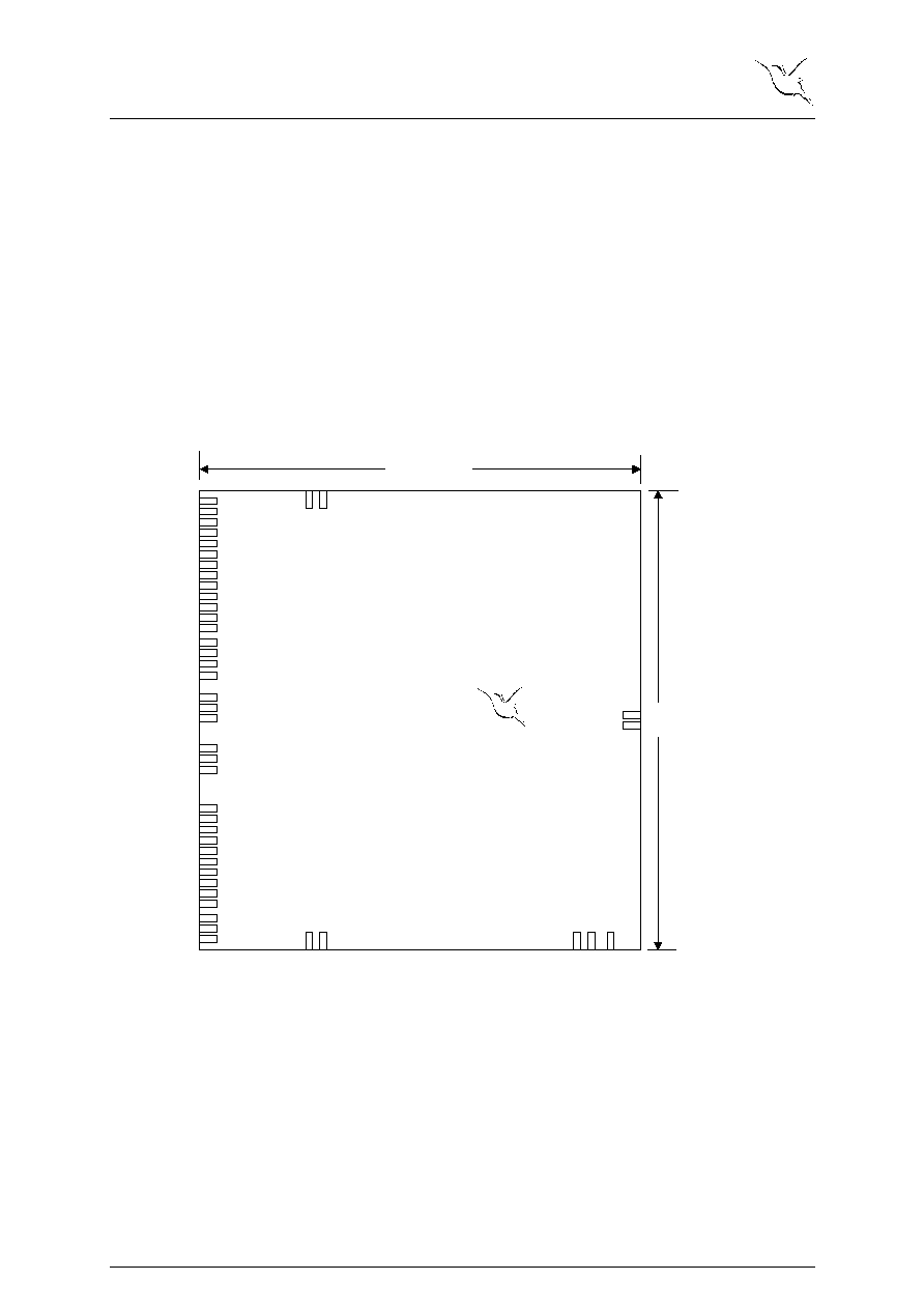
PHYSICAL DESCRIPTION
Dimensions and pin-out configuration for the core
is shown in Figure 2. The core occupies
approximately 1.6 mm
2
of silicon area, and
includes necessary shielding and guardring. It is
implemented in TSMC 0.18
µm CMOS process,
using no extra mixed signal options. All the 6
available metal layers are utilized by the core. No
fill pattern is necessary to meet TSMC density
rules, it meets all TSMC density rules on poly and
metal.
It is designed for, and verified with standard TSMC
I/O pads with ESD protection. I/O Pads are not
included in the core. Recommended pad type for
each pin, if exiting the die, is available in the
integration instruction document. This document
also contains guidelines for padring design and
package requirements.
REFP
REFN
RFLAG0[0]
RFLAG0[1]
RFLAG0[2]
BITO0[0]
BITO0[1]
BITO0[2]
BITO0[3]
BITO0[4]
BITO0[5]
BITO0[6]
BITO0[7]
BITO0[8]
BITO0[9]
INP0
VCM0
INN0
VCM1
INN1
BITO1[9]
BITO1[8]
BITO1[7]
BITO1[6]
BITO1[5]
BITO1[4]
BITO1[3]
BITO1[2]
BITO1[1]
BITO1[0]
RFLAG1[2]
RFLAG1[1]
RFLAG1[0]
nAD10110x2-18a
TOP VIEW
(Pin size and placment not to scale)
CLKBSEL
EXT
R
EF
OP
M[1]
OP
M[0]
AV
DD
1
AV
SS
AV
DD
0
AV
SS
1180
µm
1320
µm
CLKB
CLKA
CLK_OUT
INP1
Figure 2. Core dimensions and pinout configuration
PRELIMINARY PRODUCT SPECIFICATION
nAD10110x2-18a - Dual 10-bit 110 MSPS Analog-to-Digital Converter IP
Nordic VLSI
Page 7 of 13
Revision: 1.0B
THEORY OF OPERATION
General Description
Each nAD10110x2-18a converter channel employs
a fully differential pipelined architecture with
digital error correction. The pipeline has 8 stages
with a low-resolution flash at the end. Each stage
converts with the sufficient redundancy to digitally
correct for errors introduced by the preceding
stage. The first stage samples and holds the
differential analog input at the positive edge of the
conversion clock. Outputs from all stages are
combined into the final 10-bit word by the digital
correction logic.
An internal reference circuit creates the positive
and negative reference voltages, V
REFP
and V
REFN
,
that define the full-scale range of both ADC
channels. The reference voltages are generated
from internal bandgap voltage.
The fully differential architecture effectively makes
the ADC robust towards noise. It thus represents an
ideal ADC with optimum performance even in
highly integrated systems.
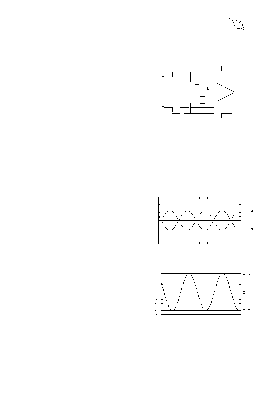
Analog Inputs
The analog input to the nAD10110x2-18a is
differential switched capacitor pipeline stage with
internal sample-and-hold functionality. It is
designed for optimum performance processing a
differential input signal with a common mode equal
to the common mode output voltage V
VCM
,
available at the VCM pin. Referring to Figure 3,
the input stage switches between the sample and
the hold phase. In the sample phase the signal
source must be able to charge the internal sample
capacitors and settle within half a clock cycle. Best
dynamic performance is obtained by matching the
source impedance of the sources driving the inputs
to ensure the common mode errors are
symmetrical. This error is further reduced by the
common mode rejection ratio of the ADC. Proper
termination of the inputs is important to maintain
input signal purity. Small resistor in series with the
inputs reduces peak currents and kickback between
the source and the input. A small capacitor between
the inputs further reduces kickback noise from the
sample-an-hold and provides dynamic charge
current. The precise values of this series resistors
and parallel capacitor should be chosen to fit the
application. For low input signal frequencies these
can be used to provide extra filtering of the input,
for high input frequencies, for example IF signals,
these components should have very small values
not to attenuate the input.
+
-
V
CM
H
H
T
T
T
1 pF
1 pF
INP
INN
Figure 3. Switched capacitor input principle
The full-scale range of the ADC is defined by the
internally generated voltage references V
REFP
and
V
REFN
,
nominally 1.275 and 0.525 V respectively.
These references are symmetrical around the the
internally generated common mode voltage V
VCM
,
nominally 0.9 V. The full-scale range V
FSR
is
defined as twice the difference between the
reference voltages V
RR
, as shown in Figure 4 and
Figure 5.
V
REFP
V
REFP
V
CM
V
INN
V
INP
V
RR
V
DD
V
SS
1.8
0
0
0.15
0.3
0.45
0.6
0.75
0.9
1.05
1.2
1.35
1.5
1.65
1.8
Figure 4. Analog input voltage swing
0.9
0.9
0.9
0.75
0.6
0.45
0.3
0.15
0
0.15
0.3
0.45
0.6
0.75
0.9
V
FSR
V
RR
V
RR
V
INP
-V
INN
Figure 5. Definition of full-scale range
Figure 4 shows a differential full-scale input signal
relative to the supply voltages.
PRELIMINARY PRODUCT SPECIFICATION
nAD10110x2-18a - Dual 10-bit 110 MSPS Analog-to-Digital Converter IP
Nordic VLSI
Page 8 of 13
Revision: 1.0B
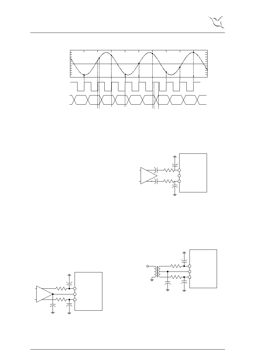
TIMING DIAGRAM
N-6
N-7
N-5
N-4
N-3
N-2
N-1
N
N+1
N-1
N
N+1
N+2
N+3
N+4
N+5
N+6
N+7
V
INP
-V
INN
t
h
t
d
CLK
BIT0[9:0]
t
AP
Figure 6. Timing diagram
Timing
Figure 6 shows the timing diagram for the
nAD10110x2-18a. The analog input voltage is
sampled at the positive edge of the conversion
clock. Latched digital output data is provided with
a pipeline delay of 5 clock cycles, and available
after one propagation delay t
d
after the rinsing edge
of the conversion clock. BITO and RFLAG have
identical timing. The two channels exhibit identical
timing.
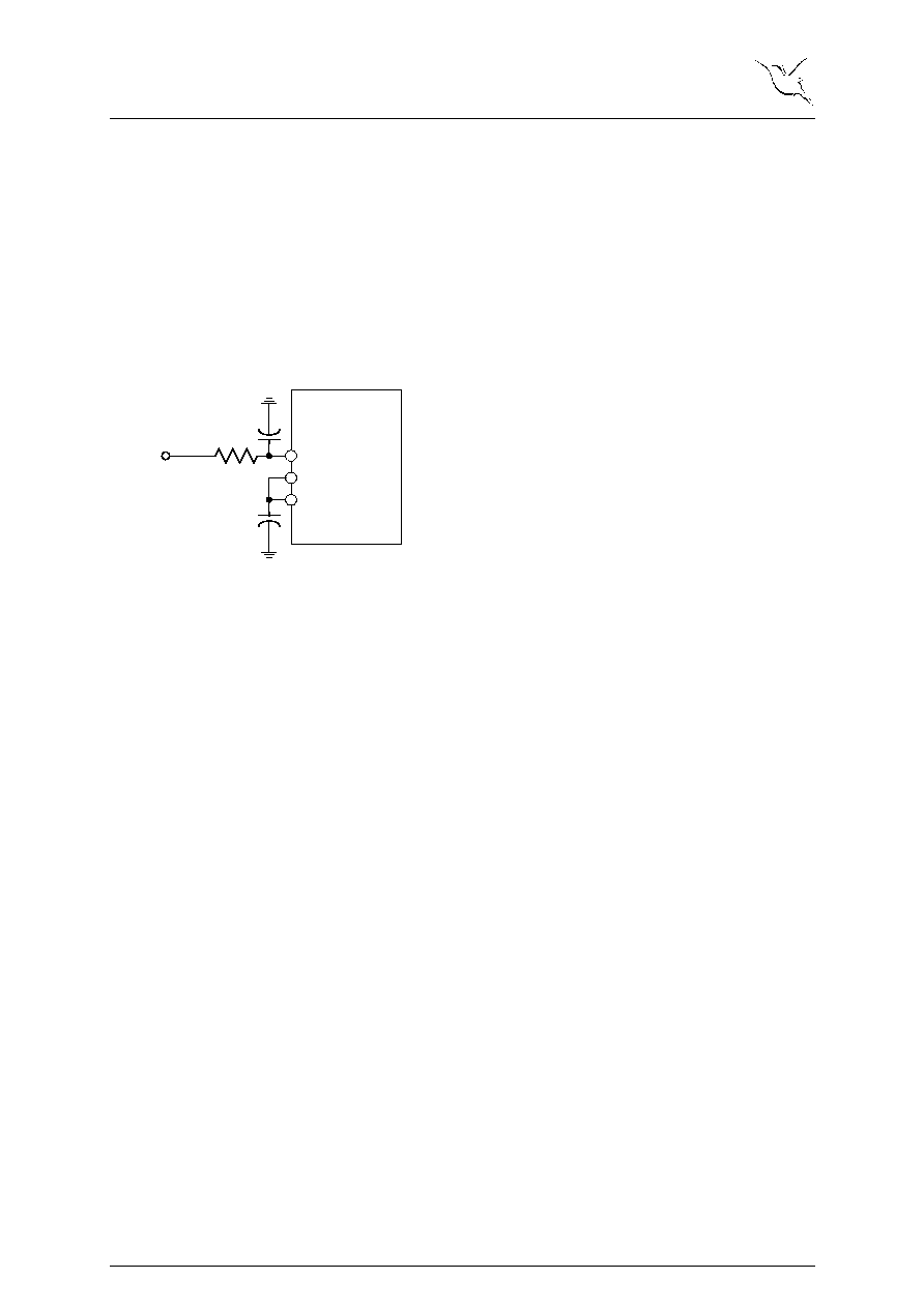
Differential Input Configuration
Optimum performance will be achieved by driving
the nAD10110x2-18a in a differential input
configuration. An example of a DC coupled input
configuration using an off-chip amplifier is shown
in Figure 7. The AD8138 differential amplifier
provides adequate performance for baseband
applications. For low IF sampling, input
frequencies in the range 50 to 100 MHz, the
AD8351 is recommended. The output common
mode of the driving amplifier should be controlled
by the common mode output of the nAD10110x2-
18a. Series resistors and small capacitors to ground
should be used to attenuate kick back noise from
the sample and hold.
+
-
Chip with
nAD IP
VCM
INN
INP
Figure 7. Differential DC coupled input using an
off-chip amplifier
Figure 8 shows an example of an AC coupled input
configuration using an off-chip amplifier. In this
configuration the common mode pin can be
bypassed on-chip, thus reducing external pin count.
+
-
Chip with
nAD IP
VCM
INN
INP
Figure 8. Differential AC coupled input using an
off-chip amplifier
An AC coupled input can also be implemented
using a transformer with a centre tapped secondary
winding. As shown in Figure 9, the center tap
should be connected to the common mode output
pin of the nAD10110x2-18a.
Chip with
nAD IP
VCM
INN
INP
V
IN
Figure 9. Differential AC coupled input using a
off-chip transformer
In order to obtain low distortion, it is important that
the transformer exhibit core saturation at full-scale.
Excellent results can be obtained with the Mini
Circuits T1-6T or T1-1T
PRELIMINARY PRODUCT SPECIFICATION
nAD10110x2-18a - Dual 10-bit 110 MSPS Analog-to-Digital Converter IP
Nordic VLSI
Page 9 of 13
Revision: 1.0B
Single-ended Input Configuration
If a single ended input is preferred, a solution based
on operational amplifiers is recommended. The
AD8138 can be used in a single ended to
differential configuration. A simple low cost
alternative is shown in Figure 10. The negative
input is connected to the common mode output, and
only the positive input is used input. In this
configuration the input full-scale range is halved,
and degradation in performance should be
expected.
Chip with
nAD IP
VCM
INN
INP
V
IN
Figure 10. Single-ended input configuration
Internal References
A nominal differential full-scale range of 1.5 V
peak-to-peak is generated by the internal voltage
reference. However for stable operation the REFP
and REFN pins should be bypassed to ground using
at least 10 nF capacitor. The internal references are
buffered with a low output impedance buffer,
which is disabled for external reference operation.
External Reference Configuration
The internal references can be overridden by
externally generated references. This can be used to
set the full-scale range between
± 0.5 to ± 0.75 V.
Setting the EXTREF signal high disables the
internal reference circuit, and an appropriate
amplifier can set the voltages at the REFP and
REFN pins. Externally generated reference must be
symmetrical about the 0.9 V common mode
voltage.
Clock Input
The nAD10110x2-18a uses both edges of the input
clock to generate internal timing signals, and thus
is sensitive to the conversion clock duty cycle. To
maintain specified performance the clock must
have 50 % duty cycle within 5 % tolerance. In
order to preserve performance at high input
frequencies, it is critical that the clock has low jitter
and steep edges. The ADC can be considered as a
mixer of the clock and the input signal.
Multiplication in the time domain is equivalent to
convolution in the frequency domain. Aperture
jitter on the clock is a wide band noise. This noise
will be sampled and effectively folded into the
output spectrum. This noise will degrade the SNDR
of the ADC.
The ideal SNDR of an N bit ADC is given by:
SNDR = 6.02
◊N + 1.76 [dB]
Which yields 62 dB for a 10-bit converter.
Degradation of the SNDR only due to the effect of
aperture jitter is given by:
SNDR
jitter
= 20log(2
F
in
rms
)
where
rms
is rms value of the conversion clock
jitter. This form of degradation applies to any
number of bits and sampling frequencies. When
considering overall system performance it should
be noted that the clock jitter is summed as root
mean square. If the conversion clock applied to the
converter has a jitter of
s
, this jitter will be added
to the internal jitter t
jitter
of the ADC. The total
degradation due to jitter is then given by:
SNR
jitter
= 20log(2
F
in
(
2
rms
+ t
2
jitter
)
Ú
�
This equation provides much insight into the noise
performance that can be expected from the ADC
with a given clock source. A second effect is
harmonic noise on the clock, generated for example
by circuitry running at a frequency different from
the sampling frequency. These frequencies will
also be mixed with the input signal and show up in
the output spectrum. Although the clock is a signal
with digital levels and transitions it should be
treated very carefully to ensure optimum dynamic
performance.
Digital Outputs
The digital output data BITO[9:0] appears in 10-bit
offset binary code at CMOS levels. Three extra bits
RFLAG[2:0] are provided to indicate out-of range
conditions. Table 8 shows the digital output coding.
A nominal full-scale range of 1.5 V peak-to-peak is
used in the table. The RFLAG[2] output indicates
that the analog input is under-range, RFLAG[1]
that the analog input is over-range. Out-of range is
indicated by RFLAG[0], which is the logical OR of
RFLAG[1] and RFLAG[2].
The digital output drivers are scaled to provide
necessary current to drive on-chip logic. For
applications that require driving of large capacitive
loads, extra buffering should be added to avoid
performance degradations.

PRELIMINARY PRODUCT SPECIFICATION
nAD10110x2-18a - Dual 10-bit 110 MSPS Analog-to-Digital Converter IP
Nordic VLSI
Page 10 of 13
Revision: 1.0B
Clock Input Mux and Output Clock
The nAD10110x2-18a provides two clock inputs
CLKA and CLKB, of which only one can be used
as the active conversion clock at the time. Active
conversion clock is selected by the CLKBSEL
signal. Table 6 shows how to set active conversion
clock with the CLKBSEL signal.
CLKBSEL
Active conversion
clock
High
CLKB
Low
CLKA
Table 6. Input clock mux control settings
A copy of the internally used conversion clock is
available at the CLK_OUT pin.
Operational Mode Control
In addition to the active mode, in which both ADC
channels are operating normally, the nAD10110x2-
18a provides standby, sleep and power down
modes. These idle modes can be used to save
power while the ADC is not required to be active.
The different modes reflects different trade-offs
between power saving and start-up time to active
mode. The start-up time is defined as the time it
takes to reach full performance in active mode
switching from the idle mode. Table 7 shows how
to set the operational mode with the input digital
control code OPM[1:0].
Mode of Operation
( both channels )
OPM[1:0]
Active
11
Standby
10
Sleep
01
Power Down
00
Table 7. Operational mode control settings
For power consumption and start-up times for the
idle modes refer to electrical specifications in Table
2 and Table 3.
Dynamic Power Scaling
The bias level of the nAD10110x2-18a is
automatically adjusted based on the conversion
rate. This means that the ADC is not just functional
at lower conversion rates than the maximum, but
the power dissipation is also continuously
minimized for the current conversion speed. The
power consumption is roughly proportional to the
conversion rate, so halving the conversion rate
roughly halves the power dissipation.
Required Off-Chip Components
In addition to components required by the specific
input configuration, a set of off-chip components is
necessary for correct operation.
The differential reference pins, REFP and REFN
must be bypassed to each other with 10 nF. The
two analog power pins, AVDD0 and AVDD1 must
be bypassed to external ground with 100 nF in
parallel with 1 nF.
DIGITAL OUTPUT CODING
Code
V
INP
-V
INN
1.5 V p-p FSR
Digital Output
BIT0[9:0]
Over-Range Indicator
RFLAG[2:0]
1023
> 0.75 V
1 111 111 111
011
512
0.75 mV
1 000 000 000
000
511
- 0.75 mV
0 111 111 111
000
0
< - 0.75 V
0 000 000 000
101
Table 8. nAD10110x2-18a digital output coding

PRELIMINARY PRODUCT SPECIFICATION
nAD10110x2-18a - Dual 10-bit 110 MSPS Analog-to-Digital Converter IP
Nordic VLSI
Page 11 of 13
Revision: 1.0B
DELIVERABLES
Upon a licensing we provide a complete set of
deliverables. It includes all necessary files for
design-in and integration, like streamfile, HDL
model, timing model and footprint files. In addition
we provide a set of documentation covering
everything from integration guidelines to
production test specification. Table 9 lists and
describes the deliverables.
ENGINEERING SUPPORT
An IP licensing also includes 40 hours of support
from our highly experienced engineers. We have
experience with integration of our IPs in broadband
communication, imaging and video chips.
Examples of areas where our support can be
valuable are:
∑ Design-in
Specification
IP configuration
Extra IP features
∑ Layout integration
Floorplanning
Signal routing and connection
Power supply strategies
Clock strategies
Padring and bond-out
∑ System Verification
LVS , DRC and Antenna check
Functional verification
Timing closure
∑ Characterization
PCB design
Test software
Test instrumentation
∑ Production test
Test strategy
Test software
CUSTOMIZATION
We also offer customization of this IP to meet extra
requirements set by your application.
COMPLETE DESIGN HANDOFF
Using the Nordic VLSI PhysicalExpress service we
are able to offer a complete design handoff. With
our extended mixed signal experience we take your
RTL code, netlist or gds2 and integrate it with our
IP. We can deliverer a complete gds2 or packaged
tested components back to you. Please refer to our
website for more details about this service.
COMPLETE DELIVERABLE LIST
Deliverable
Description
Physical Layout
Physical layout stream file in gds2 format. The stream file includes the
complete IP with necessary guardring and shielding.
Netlist
Flat spice compatible netlist for LVS and simulations.
Footprint
IP footprint in LEF format for floorplanning and placement.
Timing Models
Synopsys .lib files for timing closure.
HDL
Models
Verilog or VHDL behavioral models for system simulation and
verification.
Evaluation Board and Samples
Packaged IP samples on evaluation board for performance measurements
and prototype systems.
Application Notes
Various application notes related to the IP.
Characterization Report
Full characterization report of the packaged IP.
Integration Instructions
Guidelines for IP integration, including signal connection, recommendation
of pads and bond-out, power supply and clock strategies. Includes
description of advanced IP features and system trade-offs.
Test Specification
Guidelines for production test of the integrated IP.
Evaluation Board User Guide
Complete user guide for the evaluation board and samples.
Table 9. List of deliverables

PRELIMINARY PRODUCT SPECIFICATION
nAD10110x2-18a - Dual 10-bit 110 MSPS Analog-to-Digital Converter IP
Nordic VLSI
Page 12 of 13
Revision: 1.0B
DOCUMENT INFO
Preliminary Product Specification
nAD10110x2-18a
Product description:
Dual 10-bit 110 MSPS Analog-to-Digital Converter IP
Revision:
1.0B
Revision Date:
2003-04-10
Template ID:
1159140_045 r.1.1A
LIFE SUPPORT APPLICATIONS
These products are not designed for use in life support appliances, devices, or systems where malfunction of
these products can reasonably be expected to result in personal injury. Nordic VLSI ASA customers using or
selling these products for use in such applications do so at their own risk and agree to fully indemnify Nordic
VLSI ASA for any damages resulting from such improper use or sale.
DEFINITIONS
Data sheet status
Objective product specification
This datasheet contains target specifications for product development.
Preliminary product specification
This datasheet contains preliminary data; supplementary data may be
published from Nordic VLSI ASA later.
Product specification
This datasheet contains final product specifications.
Limiting values
Stress above one or more of the limiting values may cause permanent damage to the device. These are stress
ratings only and operation of the device at these or at any other conditions above those given in the
Specifications sections of the specification is not implied. Exposure to limiting values for extended periods may
affect device reliability.
Application information
Where application information is given, it is advisory and does not form part of the specification.
Table 10. Definitions
All rights reserved Æ. Reproduction in whole or in part is prohibited without the prior written permission of the
copyright holder.

PRELIMINARY PRODUCT SPECIFICATION
nAD10110x2-18a - Dual 10-bit 110 MSPS Analog-to-Digital Converter IP
Nordic VLSI
Page 13 of 13
Revision: 1.0B
Main Office:
Vestre Rosten 81, N-7075 Tiller, Norway
Phone: +47 72 89 89 00, Fax: +47 72 89 89 89
E-mail: datacon@nvlsi.no
Visit the Nordic VLSI ASA website at http://www.nvlsi.no