PRELIMINARY PRODUCT SPECIFICATION
nAD10120x2-13a
Dual 10-bit 120 MSPS Analog-to-Digital Converter IP
Nordic VLSI ASA - Vestre Rosten 81, N-7075 Tiller, Norway - Phone +4772898900 - Fax +4772898989
Revision: 1.0A
Page 1 of 13
2003-04-10
FEATURES
∑
Dual 10-bit ADC
∑
Up to 120 MSPS Conversion Rate
∑
Single 1.2 V Power Supply
∑
1.0 V p-p Differential Inputs
∑
Excellent Dynamic Performance
59 dBFS SNR at Fin = 10 MHz
70 dBc SFDR at Fin = 10 MHz
∑
600 MHz Analog Input Bandwidth
∑
Low Power Consumption
180mW at 120 MSPS
40 mW at 25 MSPS
∑
Excellent Gain and Phase Matching
∑
Dynamic Power Scaling
∑
Power Saving Idle Modes
∑
Internal Voltage Reference
∑
2.66 mm
2
Core Area
APPLICATIONS
∑
Communication Receive Channel
WLAN / HiperLan / 802.11x
∑
Quadrature ( I and Q ) Modulation
∑
Digital Imaging / Video
∑
TV / Video / Radio Decoders
∑
Graphic Capture
GENERAL DESCRIPTION
The nAD10120x2-13a is a monolithic, high-speed,
low power, dual channel analog-to-digital
converter silicon IP. It uses a fully differential
multistage pipeline architecture with digital error
correction to provide 10-bit accuracy from 10 to
120 MSPS conversion speed. The core includes a
wide-band sample-and-hold and an internal voltage
reference that provides a nominal full-scale range
of 1.0 V peak-to-peak. The ADC is designed for
high dynamic performance at input frequencies up
to Nyquist and beyond. It thus represents an ideal
solution for demanding applications like broadband
communication, digital imaging and multimedia.
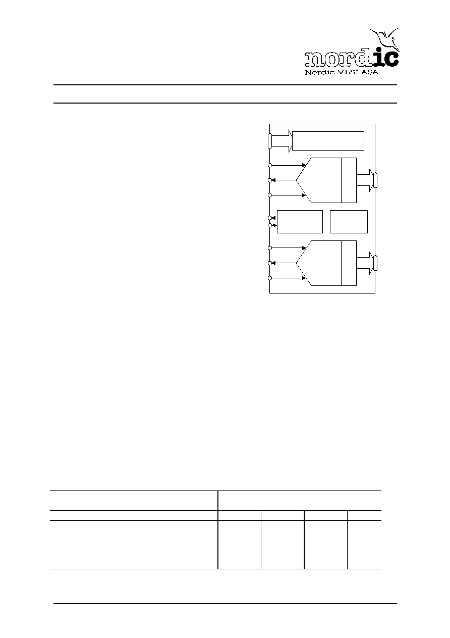
PIPELINE
ADC
DIG
I
T
A
L
CORRE
CTI
O
N
DYNAMIC
BIAS
VOLTAGE
REFERENCE
BITO0[9:0]
RFLAG0[2:0]
OPM[1:0]
CLK
EXTREF
TIMING GENERATOR
DIGITAL CONTROL
INP0
VCM0
INN0
REFP
REFN
PIPELINE
ADC
DI
GIT
A
L
CORRECT
I
O
N
BITO1[9:0]
RFLAG1[2:0]
INP1
VCM1
INN1
Figure 1. Functional block diagram
The ADC consumes only 180 mW at 120 MSPS
operation. Dynamic power scaling means that the
power consumption is scaled with the operating
frequency resulting in only 40 mW consumption at
25 MSPS operation. Combined with power saving
idle modes the ADC is suitable for battery powered
devices. Output data is available in a binary offset
coded format. Three out-of-range indicator bits are
also available for determining if the input signal is
over-range, under-range or out-of-range.
Implemented in a generic 0.13
µ
m CMOS process,
operating from a single 1.2 V supply and
employing a fully differential architecture it
represents an ideal ADC for highly integrated
mixed-signal systems.
QUICK REFERENCE DATA
IP Type / Technology
Hard Macro / TSMC Generic, 8 Metal 0.18
µ
m CMOS
IP Area / Dimensions
2.66 mm
2
/ 1.40
◊
1.90 mm
Parameter
Min.
Typ.
Max.
Unit
Supply Voltage
1.1
1.2
1.2
V
Power Dissipation, @ F
CLK
= 110 MHz
160
mW
Differential Non Linearity
±
0.5
LSB
Integral Non Linearity
±
1.0
LSB
Signal-to-Noise Ration, F
IN
= 10 MHz
59
dBFS
Spurious-Free-Dynamic Range, F
IN
= 10 MHz
70
dBc
Table 1. nAD10120x2-13a quick reference data
PRELIMINARY PRODUCT SPECIFICATION
nAD10120x2-13a - Dual 10-bit 120 MSPS Analog-to-Digital Converter IP
Nordic VLSI
Page 2 of 13
Revision: 1.0A
ELECTRICAL SPECIFICATIONS
DC SPECIFICATIONS
( At T
A
= 25 ∫C, V
AVDD
= V
VDD
= 1.2 V, F
CLK
= 120 MHz, F
IN
= 10 MHz, internal references, differential full-
scale input signal, 50 % duty cycle clock, and 10nF reference decoupling, data per channel, unless otherwise
noted )
Symbol
Parameter (condition)
Test
level
Min.
Typ.
Max.
Unit
DC ACCURACY
N
Resolution
10
Bits
NMC
No Missing Codes Guaranteed
10
Bits
INL
Integral Non Linearity
±
1
LSB
DNL
Differential Non Linearity
±
0.5
LSB
G
Gain Error
±
1.0
% FSR
Gain Matching between channel 0 and 1
0.5
% FSR
V
OS
Offset Error
±
1.0
% FSR
ANALOG INPUT
V
FSR
Input Differential Voltage Range
±
0.5
V
V
VCM,EXT
Input Common Mode Voltage
0.6
0.65
0.7
V
Input Impedance
1.5
pF
AIBW
Analog Input Bandwidth
600
MHz
REFERENCE VOLTAGES
V
REFP
Internal Positive Voltage Reference
0.9
V
V
REFN
Internal Negative Voltage Reference
0.5
V
V
RR
Internal Reference Range
0.5
V
FSR
Internal Differential Full-scale Range
1.0
V p-p
V
VCM
Internal Reference Common Mode Voltage
0.65
V
Internal Voltage Reference Drift
100
ppm /
∞
C
V
RR,EXT
External Reference Range
0.25
0.5
V
FSR
EXT
External Differential Full Scale Range
0.5
1.0
V p-p
V
RCM,EXT
External Reference Common Mode Voltage
0.65
V
POWER SUPPLY
V
AVDD
Positive Analog Supply Voltage
1.1
1.2
1.3
V
V
VDD
Positive Digital Supply Voltage
1.1
1.2
1.3
V
V
SS
Negative Supply Voltage
GND
I
DD
Supply Current, Active
1
150
mA
Supply Current, Standby
2.2
mA
Supply Current, Sleep
1.7
mA
Supply Current, Power down
2.2
µ
A
P
DD
Power Dissipation, Active
1
180
mW
Power Dissipation, Standby
4
mW
Power Dissipation, Sleep
3
mW
Power Dissipation, Power down
4
µ
W
OPERATING CONDITIONS
T
A
Junction Operating Temperature
-40
125
∞
C
Table 2. nAD10120x2-13a DC Specifications
1
Both channels active
PRELIMINARY PRODUCT SPECIFICATION
nAD10120x2-13a - Dual 10-bit 120 MSPS Analog-to-Digital Converter IP
Nordic VLSI
Page 3 of 13
Revision: 1.0A
DYNAMIC SPECIFICATIONS
( At T
A
= 25 ∫C, V
AVDD
= V
VDD
= 1.2 V, F
CLK
= 120 MHz, F
IN
= 10 MHz, internal references, differential full-
scale input signal, 50 % duty cycle clock, and 10nF reference decoupling, data per channel, unless otherwise
noted)
Symbol
Parameter (condition)
Test
level
Min.
Typ.
Max.
Unit
SWITCHING PERFORMANCE
F
CLK,MAX
Maximum Conversion Rate
120
MSPS
F
CLK,MIN
Minimum Conversion Rante
10
MSPS
Input Clock Duty Cycle
45
50
55
%
t
pd
Pipeline Delay ( Latency )
6
clocks
t
d
Output Data Delay Time
2
ns
t
h
Output Data Hold Time
1
ns
t
ad
Aperture Delay Time
0.9
ns
t
jitter
Aperture Uncertainty ( Jitter )
1.5
ps rms
t
standby
Start-up Time from Standby Mode
5
clocks
t
sleep
Start-up Time from Sleep Mode
0.5
µ
s
t
power down
Start-up Time from Power Down Mode
5
µ
s
t
out-of-range
Out-of-Range Recovery Time
SNR
SIGNAL-TO-NOISE RATIO
120 MSPS, F
IN
= 10 MHz
59
dBFS
120 MSPS, F
IN
= 40 MHz
58.5
dBFS
120 MSPS, F
IN
= 72 MHz
58
dBFS
SINAD
SIGNAL-TO-NOISE-AND DISTORTION
RATIO
120 MSPS, F
IN
= 10 MHz
58
dBFS
120 MSPS, F
IN
= 40 MHz
53
dBFS
120 MSPS, F
IN
= 72 MHz
50
dBFS
SFDR
SPURIOUS FREE DYNAMIC RANGE
120 MSPS, F
IN
= 10 MHz
70
dBc
120 MSPS, F
IN
= 40 MHz
62
dBc
120 MSPS, F
IN
= 72 MHz
52
ENOB
EFFECTIVE NUMBER OF BITS
120 MSPS, F
IN
= 5 MHz
9.6
Bit
120 MSPS, F
IN
= 10 MHz
9.34
Bit
120 MSPS, F
IN
= 40 MHz
8.5
Bit
120 MSPS, F
IN
= 72 MHz
8.0
Bit
CHANNEL ISOLATION
120 MSPS, F
IN
= 5 MHz
50
dBc
Table 3. nAD10120x2-13a Dynamic Specifications

PRELIMINARY PRODUCT SPECIFICATION
nAD10120x2-13a - Dual 10-bit 120 MSPS Analog-to-Digital Converter IP
Nordic VLSI
Page 4 of 13
Revision: 1.0A
DEFINITIONS OF SPECIFICATIONS
Integral Non Linearity ( INL )
The deviation of the ADC transfer function from
the ideal transfer function. The ideal transfer
function is defined as a straight line between the
end points of the transfer characteristic corrected
for gain and offset. INL for each code is calculated
at the code transitions.
Differential Non Linearity ( DNL )
In an ideal ADC every code transition to its
neighbours equals to 1 LSB. DNL is the deviation
of each code transition from the ideal value.
Gain Error
The deviation of the actual difference between the
first and last code transition and the ideal
difference.
Channel Gain Matching
Gain difference between the two channels.
Offset Error
Mid code ideally occurs for zero differential input.
The offset error is the differential input voltage that
gives mid code.
Analog Input Bandwidth
The analog input frequency for which the measured
input signal power has dropped by 3 dB.
Temperature Drift
The temperature drift specifies the maximum
change from the nominal junction temperature to
the minimum and maximum junction temperature.
Maximum Conversion Rate
The maximum conversion rate is the conversion
rate at which electrical specifications are tested.
Minimum Conversion Rate
The minimum conversion rate is the slowest
conversion rate where the ADC is functional.
Pipeline Delay ( Latency )
The pipeline delay is the time it takes from a
sample is taken at the input to the sample is
converted and put on the digital output.
Output Data Delay Time
Output data delay time is the time from the clock
edge that defines valid output data to all data
outputs have reached valid logical levels for the
next data sample.
Output Data Hold Time
Output data hold time is the time from the clock
edge that defines valid output data to the output
data is no longer valid.
Aperture Delay Time
The delay between the sampling clock edge and the
time when the input signal is held for conversion.
Aperture Uncertainty ( Jitter )
Aperture uncertainty or jitter is the variation of the
aperture delay time for successive samples.
Clock Duty Cycle
The fraction of the time the clock spends above the
logic threshold.
Start-up Time from Idle Mode
The time it takes to reach full performance after a
transition from an idle mode to active mode.
Out of Range Recovery Time
The time required for the ADC to return to
specified characteristics after an out-of-range
sample.
Signal-to-Noise Ratio ( SNR )
SNR is the rms ratio of the measured input signal
to the sum of all other spectral components
excluding the dc and the first eight harmonics.
Spurious-Free Dynamic Range ( SFDR )
SFDR is the amplitude difference between the
measured input signal and the highest harmonic
component.
Signal-to-Noise and Distortion Ratio ( SNDR )
SNDR is the rms ratio of the measured input signal
to the sum of all other spectral harmonics
excluding the dc component.
Effective Number of Bits ( ENOB )
Effective number of bits specifies the total rms
noise in terms of bits of resolution the ADC
effectively performs. Generally ENOB depends on
the amplitude and frequency of the input signal
used to test it. The ENOB can be calculated
directly from the SNDR as follows:
6.02
1.76
SNDR
ENOB
-
=
Channel Isolation
Coupling into one channel with a ≠40 dBFS input
signal from the other channel driven by a full-scale
input signal.

PRELIMINARY PRODUCT SPECIFICATION
nAD10120x2-13a - Dual 10-bit 120 MSPS Analog-to-Digital Converter IP
Nordic VLSI
Page 5 of 13
Revision: 1.0A
ABSOLUTE MAXIMUM RATINGS
1
Pin / Condition
Min
Max
Unit
All pins referred to AVSS pin
-0.2
1.5
V
Operating Junction Temperature
-40
125
∞
C
Storage Temperature
-65
125
∞
C
Table 4. Absolute maximum ratings
EXPLANATION OF TEST LEVELS
Test Level I:
100% production tested at +25∞C
Test Level II:
100% production tested at +25∞C and sample tested at specified temperatures
Test Level III:
Sample tested only
Test Level IV:
Parameter is guaranteed by design and characterization testing
Test Level V:
Parameter is typical value only
Test Level VI:
100% production tested at +25∞C. Guaranteed by design and characterization testing for
industrial temperature range
COMPLETE PINOUT LIST
Name
Type
1)
Description
INP0, INN0
AI
Differential Voltage Inputs, Channel 0
INP1, INN1
AI
Differential Voltage Inputs, Channel 1
VCM0
AO
Common Mode Voltage Output, Channel 0
VCM1
AO
Common Mode Voltage Output, Channel 1
REFP, REFN
AB
Differential Voltage References
CLK0
DI
Conversion Clock, Channel 0
CLK1
DI
Conversion Clock, Channel 1
BITO0[9:0]
DO
Digital Output Code, Channel 0. BITO0[9] is MSB, BITO0[0] is LSB
BITO1[9:0]
DO
Digital Output Code, Channel 1. BITO1[9] is MSB, BITO1[0] is LSB
RFLAG0[2:0]
DO
Digital Over-Range Indicator Output Code, Channel 0
RFLAG1[2:0]
DO
Digital Over-Range Indicator Output Code, Channel 1
OPM[1:0]
DI
Operational Mode Control Input Code
OECTRL0
DI
Enables Channel 0 Digital Outputs when high
OECTRL1
DI
Enables Channel 1 Digital Outputs when high
AVDD0
AP
Positive 1.2 V Supply, Channel 0
AVDD1
AP
Positive 1.2 V Supply, Channel 1
VDD
DP
Positive 1.2 V Supply, Digital
AVSS
AG
Ground
1)
D = Digital, A = Analog, I = In, O = Out, B = Bidirectional, T = Tristate, P = Power, G = Ground.
Table 5. nAD10120x2-13a pinout list
1
Stress above one or more of the limiting values may cause permanent damage to the device