PRODUCT SPECIFICATION
Main office: Nordic VLSI ASA - Vestre Rosten 81, N-7075 Tiller, Norway - Phone +4772898900 - Fax +4772898989
Revision: 3.0
Page 1 of 11
August 31
st
2001
10-Bit 30MSPS Sampling
Analog-to-Digital Converter
FEATURES
∑
1.8V power supply
∑
SNR typ 60dB for (f
in
= 10MHz)
∑
Low power (21mW @ 1.8V and
30MSPS)
∑
Frequency dependent biasing
∑
Internal Sample/Hold
∑
Differential input
∑
Low input capacitance
∑
Power Down and Sleep Mode
APPLICATIONS
∑
Imaging
∑
Test equipment
∑
Computer scanners
∑
Wireless communication
∑
Powerline communication
∑
Set top boxes
∑
Video products
GENERAL DESCRIPTION
The nAD1030-18 is a compact, high-speed, low power 10-bit monolithic analog-to-
digital converter, implemented in a 0.18
µ
m single poly CMOS process with MiM
capacitor option. The converter includes a high bandwidth sample and hold. Using
internal references, the full scale range is
±
0.75V. The full scale range can be set
between
±
0.5V and
±
0.75V using external references. It operates from a single 1.8V
supply. Its low distortion and high dynamic range offers the performance needed for
demanding imaging, multimedia, telecommunications and instrumentation
applications. The bias current level for the ADC is automatically adjusted based on
the clock input frequency. Hence, the power dissipation of the device is continuously
minimised for the current operation frequency.
QUICK REFERENCE DATA
Symbol
Parameter
Conditions
Min.
Typ.
Max.
Unit
V
DD
Supply voltage
1.6
1.8
2.0
V
I
DD
Supply current
(30 MSPS)
11.6
mA
P
D
Power dissipation
(10 MSPS)
Except digital
output drivers
8
mW
P
D
Power dissipation
(30 MSPS)
Except digital
output drivers
21
mW
DNL
Differential
nonlinearity
f
IN
=0.9991MHz
±0.5
LSB
INL
Integral nonlinearity
f
IN
=0.9991MHz
±
0.75
LSB
f
S
Conversion rate
30
MHz
N
Resolution
10
bit
Table 1. Quick reference data
nAD1030-18
PRODUCT SPECIFICATION
nAD1030-18 10 Bit 30 MSPS Sampling ADC IP
Main office: Nordic VLSI ASA - Vestre Rosten 81, N-7075 Tiller, Norway - Phone +4772898900 - Fax +4772898989
Revision: 3.0
Page 2 of 11
August 31
st
2001
GENERAL DESCRIPTION (Continued)
The nAD1030-18 has a pipelined architecture - resulting in low input capacitance.
Digital error correction of the 9 most significant bits ensures good linearity for input
frequencies approaching Nyquist. The nAD1030-18 is compact. The core occupies
less than 0.9mm
2
of die area in a standard single poly 0.18
µ
m CMOS process. The
fully differential architecture makes it insensitive to substrate noise. Thus it is ideal as
a mixed signal ASIC macro cell.
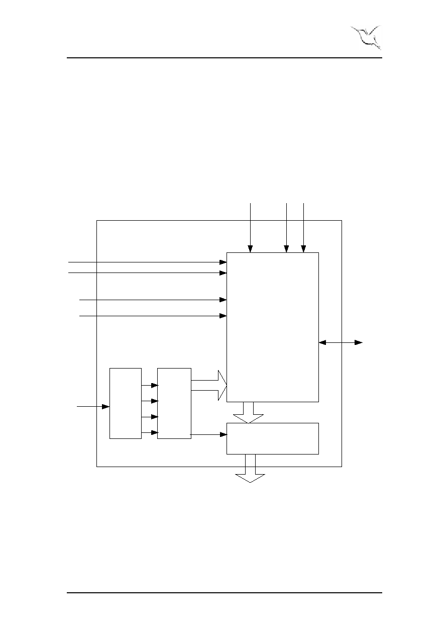
BLOCK DIAGRAM
Figure 1. Block diagram nAD1030-18
ANALOG
CORR_LOG
ANC
L
OC
K
BIT<9:0>
IN_CORR<17:0>
CKBUS<3:0>
CLOCK
INN
INP
REFP
REFN
BIAS0
BIAS1
C
L
OC
KBU
F
EXTREF
CKCORR<1:0>
CK0
CK0B
CK2
CK2B
VCM
PRODUCT SPECIFICATION
nAD1030-18 10 Bit 30 MSPS Sampling ADC IP
Main office: Nordic VLSI ASA - Vestre Rosten 81, N-7075 Tiller, Norway - Phone +4772898900 - Fax +4772898989
Revision: 3.0
Page 3 of 11
August 31
st
2001
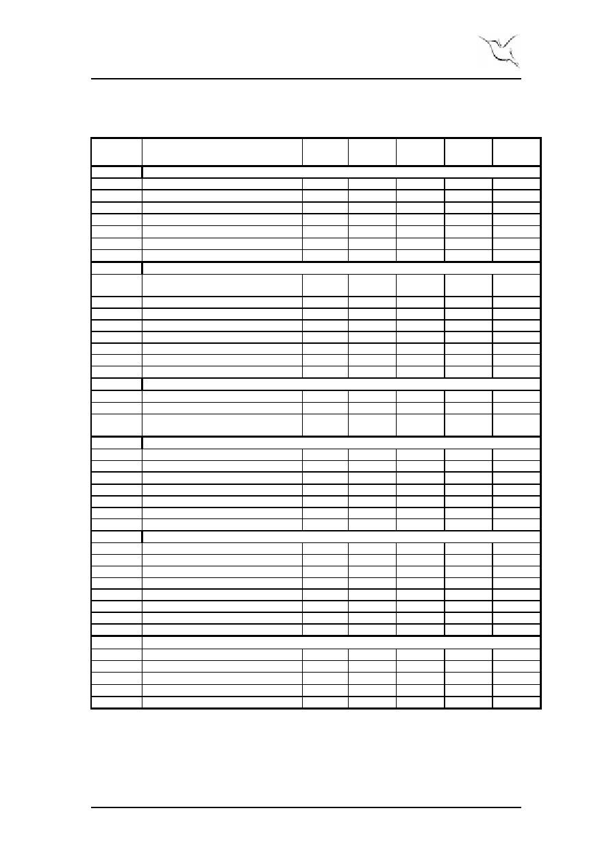
ELECTRICAL SPECIFICATIONS
(
At T
A
= 25
∞
C, V
DD
= 1.8V, Sampling Rate = 30MHz, Input frequency = 10MHz, Differential input
signal, 50% duty cycle clock unless otherwise noted
)
Symbol Parameter (condition)
Test
Level
Min.
Typ.
Max.
Units
DC Accuracy
DNL
Differential Nonlinearity
f
IN
= 0.9991 MHz
IV
±
0.5
LSB
INL
Integral Nonlinearity
f
IN
= 0.9991 MHz
IV
±
0.75
LSB
V
OS
Midscale offset
±
1
%FS
CMRR
Common Mode Rejection Ratio
-59
dB
G
Gain Error
±
1
%FS
Dynamic Performance
SNR
Signal to Noise Ratio (without
harmonics)
f
IN
= 10 MHz
IV
56
60
dBFS
f
IN
= 40 MHz
IV
55
58.5
dBFS
SINAD
Signal to Noise and Distortion Ratio
f
IN
= 10 MHz
IV
59
dBFS
SFDR
Spurious Free Dynamic Range
f
IN
= 10 MHz
IV
67
dB
f
IN
= 40 MHz
IV
57
dB
Analog Input
V
FSR
Input Voltage Range (differential)
IV
±
0.75
V
V
CMI
Common mode input voltage
IV
0.9
V
C
INA
Input Capacitance (from each input to
ground)
1.5
pF
Reference Voltages
V
REFNI
Internal reference voltage on pin 10
IV
0.525
V
V
REFPI
Internal reference voltage on pin 11
IV
1.275
V
Internal reference voltage drift
100
ppm/
∞
C
V
REFNO
Negative Input Voltage
IV
0.525
V
V
REFPO
Positive Input Voltage
IV
1.275
V
V
REFP
-V
REFN
Reference input voltage range
1)
IV
0.75
V
V
CM
Common mode output voltage
IV
0.9
V
Switching Performance
F
S
Conversion Rate
IV
30
MSPS
Pipeline Delay
IV
6
Clocks
t
AP
Aperture delay, IP
V
0.9
ns
t
h
Output hold time, IP
V
0.5
ns
t
d
Output delay time, IP
V
2.5
ns
t
AP
Aperture delay, with bonding pad
V
1.0
ns
t
h
Output hold time, with bonding pad
V
1.0
ns
t
d
Output delay time, with bonding pad
V
4.0
ns
Digital Inputs
V
IL
Logic "0" voltage
IV
0.4
V
V
IH
Logic "1" voltage
IV
AV
DD
-0.4
V
I
IL
Logic "0" current (V
I
=V
SS
)
IV
±
10
µ
A
I
IH
Logic "1" current (V
I
=V
DD
)
IV
±
10
µ
A
C
IND
Input Capacitance
IV
5
pF
(table continued on next page)
PRODUCT SPECIFICATION
nAD1030-18 10 Bit 30 MSPS Sampling ADC IP
Main office: Nordic VLSI ASA - Vestre Rosten 81, N-7075 Tiller, Norway - Phone +4772898900 - Fax +4772898989
Revision: 3.0
Page 4 of 11
August 31
st
2001
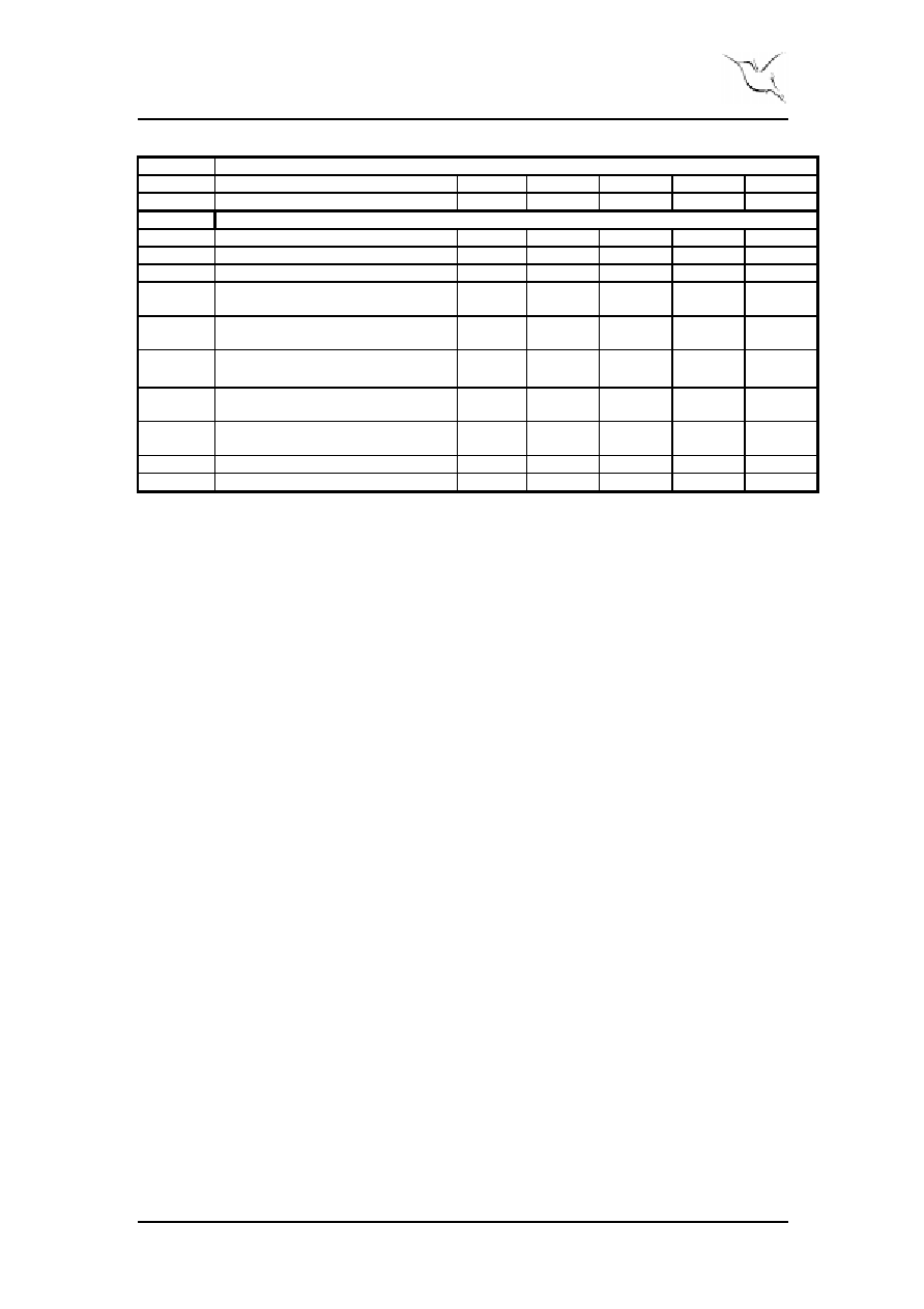
Digital Outputs
V
OL
Logic "0" voltage (I = 2 mA)
IV
0.2
0.4
V
V
OH
Logic "1" voltage (I = 2 mA)
IV
85% OV
DD
90% OV
DD
V
Power Supply
V
DD
Supply voltage
V
1.6
1.8
2.0
V
I
DD
Supply current (except digital output)
IV
mA
V
SS
Supply voltage
GND
P
D
Power dissipation (except digital output)
(10 MSPS)
IV
8
mW
P
D
Power dissipation (except digital output)
(30 MSPS)
IV
21
mW
P
D
Power dissipation (except digital output)
Power Down Mode
2)
IV
45
µW
P
D
Power dissipation (except digital output)
Sleep Mode
IV
655
µW
AV
DD
-
DV
DD1
Analog power ≠ digital power pins
-0.2
+0.2
V
OV
DD
Output driver supply voltage
1.6
1.8
2.0
V
T
Ambient operating temperature
-40
+85
∞
C
Table 2. Electrical specifications
1)
See Figure 5.
2)
Power Down Mode is only available for IP version of nAD1030-18.
Test Levels
Test Level I: 100% production tested at +25∞C
Test Level II: 100% production tested at +25∞C and sample tested at specified
temperatures
Test Level III: Sample tested only
Test Level IV: Parameter is guaranteed by design and characterization testing
Test Level V: Parameter is typical value only
Test Level VI: 100% production tested at +25∞C. Guaranteed by design and
characterization testing for industrial temperature range
ABSOLUTE MAXIMUM RATINGS
Supply voltages
AV
DD
............................- 0.2V to +2.2V
DV
DD1
..................- 0.2V to V
DD
+ 0.2V
OV
DD
...................- 0.2V to V
DD
+ 0.2V
Input voltages
Analog In.......... - 0.2V to AV
DD
+ 0.2V
Digital In..............- 0.2V to V
DD
+ 0.2V
REF
P
................. - 0.2V to AV
DD
+ 0.2V
REF
N
................. - 0.2V to AV
DD
+ 0.2V
CLOCK ...............- 0.2V to V
DD
+ 0.2V
Temperatures
Operating Temperature ....-40 to +85
∞
C
Storage Temperature.. ... - 65 to +125
∞
C
Note: Stress above one or more of the limiting values may cause permanent damage
to the device.

PRODUCT SPECIFICATION
nAD1030-18 10 Bit 30 MSPS Sampling ADC IP
Main office: Nordic VLSI ASA - Vestre Rosten 81, N-7075 Tiller, Norway - Phone +4772898900 - Fax +4772898989
Revision: 3.0
Page 5 of 11
August 31
st
2001
PIN FUNCTIONS
Pin Name
Description
INP INN
Differential input signal pins. Common mode voltage: 0.9V
REFP REFN
Reference input pins. Bypass with 100nF capacitors close to the pins. See Application
Information below.
BIAS0, BIAS1
Digital inputs for max. sampling rate programming.
BIAS1=0, BIAS0=0: Sleep mode (power save)
BIAS1=0, BIAS0=1: - 12.5% bias
BIAS1=1, BIAS0=0: +12.5% bias
BIAS1=1, BIAS0=1: Typ. Bias
The bias setting is automatically performed based on the clock input frequency. This
function should be used ONLY if another bias setting than typical must be used.
CLOCK
Clock input
VCM
Common mode voltage output
BIT9 - BIT0
Digital outputs ( MSB to LSB)
OR
OverRange. High if all outputs are zeros or ones. Available on IP.
OUTEN
Enable digital outputs (Keep low for active outputs)
EXTREF
Disable internal references (Keep low for internal references)
PD
Power Down (Keep low for normal operation) Available on IP or with bonding option.
V
DD
Power pins for on chip power
V
SS
Ground pins
OV
DD
Power pins for output drivers
Table 3. Pin functions
PIN ASSIGNMENT
nAD1030-18
28 PIN SSOP
1
2
3
4
5
6
7
8
9
10
11
12
13
14
BIT9
BIT8
BIT7
BIT6
BIT5
OV
DD
OV
DD
V
SS
V
SS
BIT4
BIT3
BIT2
BIT1
BIT0
28
27
26
25
24
23
22
21
20
19
18
17
16
15
VCM
BIAS1
REFN
REFP
BIAS0
CLOCK
OUTEN
INP
INN
V
DD
V
SS
EXTREF
V
DD
V
SS
Figure 2. Pin assignment for the 28 pin package used for samples