PRODUCT SPECIFICATION
Main office: Nordic VLSI ASA - Vestre Rosten 81, N-7075 Tiller, Norway - Phone +4772898900 - Fax +4772898989
Revision: 3.0
Page 1 of 11
August 31
st
2001
10-Bit 50MSPS Sampling
Analog-to-Digital Converter
FEATURES
∑
1.8V power supply
∑
SNR typ 59dB for (f
in
= 10MHz)
∑
Low power (33mW @ 1.8V and
50MSPS)
∑
Frequency dependent biasing
∑
Internal Sample/Hold
∑
Differential input
∑
Low input capacitance
∑
Power Down and Sleep Mode
APPLICATIONS
∑
Imaging
∑
Test equipment
∑
Computer scanners
∑
Wireless communication
∑
Powerline communication
∑
Set top boxes
∑
Video products
GENERAL DESCRIPTION
The nAD1050-18 is a compact, high-speed, low power 10-bit monolithic analog-to-
digital converter, implemented in a 0.18
µ
m single poly CMOS process with MiM
capacitor option. The converter includes a high bandwidth sample and hold. Using
internal references, the full scale range is
±
0.75V. The full scale range can be set
between
±
0.5V and
±
0.75V using external references. It operates from a single 1.8V
supply. Its low distortion and high dynamic range offers the performance needed for
demanding imaging, multimedia, telecommunications and instrumentation
applications. The bias current level for the ADC is automatically adjusted based on
the clock input frequency. Hence, the power dissipation of the device is continuously
minimised for the current operation frequency.
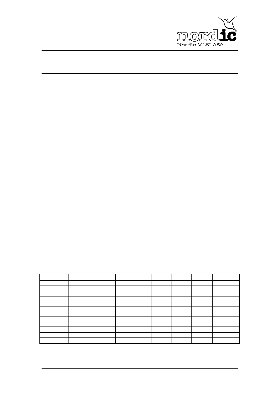
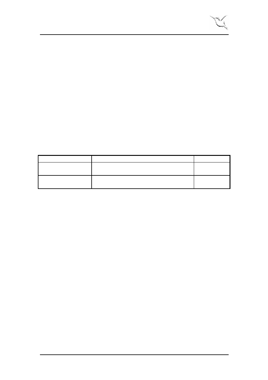
QUICK REFERENCE DATA
Symbol
Parameter
Conditions
Min.
Typ.
Max.
Unit
V
DD
Supply voltage
1.6
1.8
2.0
V
I
DD
Supply current
(50 MSPS)
18.3
mA
P
D
Power dissipation
(10 MSPS)
Except digital
output drivers
8
mW
P
D
Power dissipation
(50 MSPS)
Except digital
output drivers
33
mW
DNL
Differential
nonlinearity
f
IN
=0.9991MHz
±0.5
LSB
INL
Integral nonlinearity
f
IN
=0.9991MHz
±
0.75
LSB
f
S
Conversion rate
50
MHz
N
Resolution
10
bit
Table 1. Quick reference data
nAD1050-18
PRODUCT SPECIFICATION
nAD1050-18 10 Bit 50 MSPS Sampling ADC IP
Main office: Nordic VLSI ASA - Vestre Rosten 81, N-7075 Tiller, Norway - Phone +4772898900 - Fax +4772898989
Revision: 3.0
Page 2 of 11
August 31
st
2001
GENERAL DESCRIPTION (Continued)
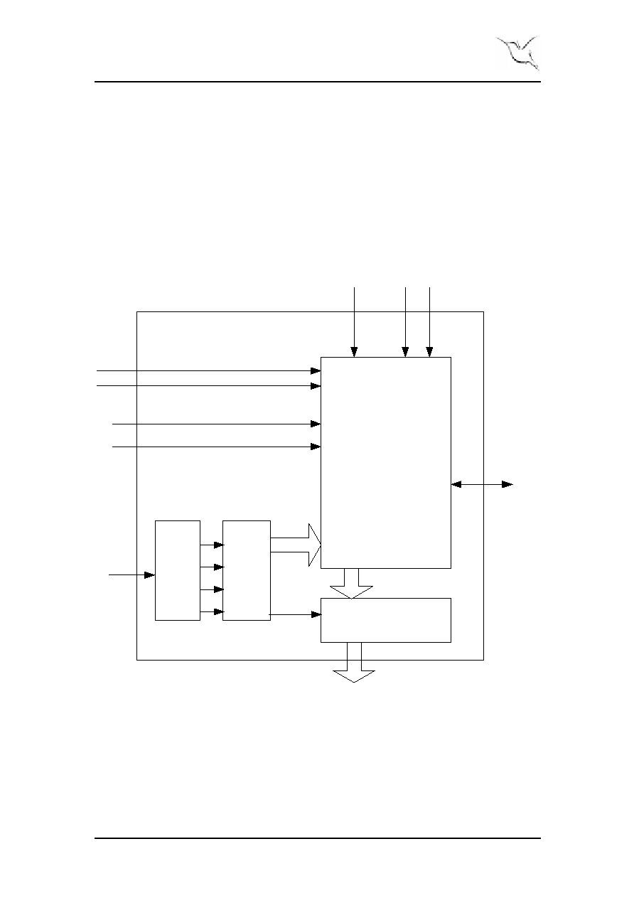
The nAD1050-18 has a pipelined architecture - resulting in low input capacitance.
Digital error correction of the 9 most significant bits ensures good linearity for input
frequencies approaching Nyquist. The nAD1050-18 is compact. The core occupies
less than 0.9mm
2
of die area in a standard single poly 0.18
µ
m CMOS process. The
fully differential architecture makes it insensitive to substrate noise. Thus it is ideal as
a mixed signal ASIC macro cell.
BLOCK DIAGRAM
Figure 1. Block diagram nAD1050-18
ANALOG
CORR_LOG
ANC
L
OC
K
BIT<9:0>
IN_CORR<17:0>
CKBUS<3:0>
CLOCK
INN
INP
REFP
REFN
BIAS0
BIAS1
C
L
OC
KBU
F
EXTREF
CKCORR<1:0>
CK0
CK0B
CK2
CK2B
VCM
PRODUCT SPECIFICATION
nAD1050-18 10 Bit 50 MSPS Sampling ADC IP
Main office: Nordic VLSI ASA - Vestre Rosten 81, N-7075 Tiller, Norway - Phone +4772898900 - Fax +4772898989
Revision: 3.0
Page 3 of 11
August 31
st
2001
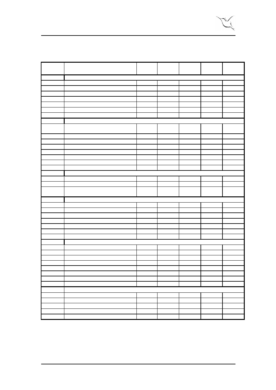
ELECTRICAL SPECIFICATIONS
(
At T
A
= 25
∞
C, V
DD
= 1.8V, Sampling Rate = 50MHz, Input frequency = 10MHz, Differential input
signal, 50% duty cycle clock unless otherwise noted
)
Symbol Parameter (condition)
Test
Level
Min.
Typ.
Max.
Units
DC Accuracy
DNL
Differential Nonlinearity
f
IN
= 0.9991 MHz
IV
±
0.5
LSB
INL
Integral Nonlinearity
f
IN
= 0.9991 MHz
IV
±
0.75
LSB
V
OS
Midscale offset
±
1
%FS
CMRR
Common Mode Rejection Ratio
-59
dB
G
Gain Error
±
1
%FS
Dynamic Performance
SNR
Signal to Noise Ratio (without
harmonics)
f
IN
= 10 MHz
IV
56
59
dBFS
f
IN
= 40 MHz
IV
55
58.5
dBFS
SINAD
Signal to Noise and Distortion Ratio
f
IN
= 10 MHz
IV
59
dBFS
SFDR
Spurious Free Dynamic Range
f
IN
= 10 MHz
IV
65
dB
f
IN
= 40 MHz
IV
57
dB
Analog Input
V
FSR
Input Voltage Range (differential)
IV
±
0.75
V
V
CMI
Common mode input voltage
IV
0.9
V
C
INA
Input Capacitance (from each input to
ground)
1.5
pF
Reference Voltages
V
REFNI
Internal reference voltage on pin 10
IV
0.525
V
V
REFPI
Internal reference voltage on pin 11
IV
1.275
V
Internal reference voltage drift
100
ppm/
∞
C
V
REFNO
Negative Input Voltage
IV
0.525
V
V
REFPO
Positive Input Voltage
IV
1.275
V
V
REFP
-V
REFN
Reference input voltage range
1)
IV
0.75
V
V
CM
Common mode output voltage
IV
0.9
V
Switching Performance
F
S
Conversion Rate
IV
50
MSPS
Pipeline Delay
IV
6
Clocks
t
AP
Aperture delay, IP
V
0.9
ns
t
h
Output hold time, IP
V
0.5
ns
t
d
Output delay time, IP
V
2.5
ns
t
AP
Aperture delay, with bonding pad
V
1.0
ns
t
h
Output hold time, with bonding pad
V
1.0
ns
t
d
Output delay time, with bonding pad
V
4.0
ns
Digital Inputs
V
IL
Logic "0" voltage
IV
0.4
V
V
IH
Logic "1" voltage
IV
AV
DD
-0.4
V
I
IL
Logic "0" current (V
I
=V
SS
)
IV
±
10
µ
A
I
IH
Logic "1" current (V
I
=V
DD
)
IV
±
10
µ
A
C
IND
Input Capacitance
IV
5
pF
(table continued on next page)
PRODUCT SPECIFICATION
nAD1050-18 10 Bit 50 MSPS Sampling ADC IP
Main office: Nordic VLSI ASA - Vestre Rosten 81, N-7075 Tiller, Norway - Phone +4772898900 - Fax +4772898989
Revision: 3.0
Page 4 of 11
August 31
st
2001
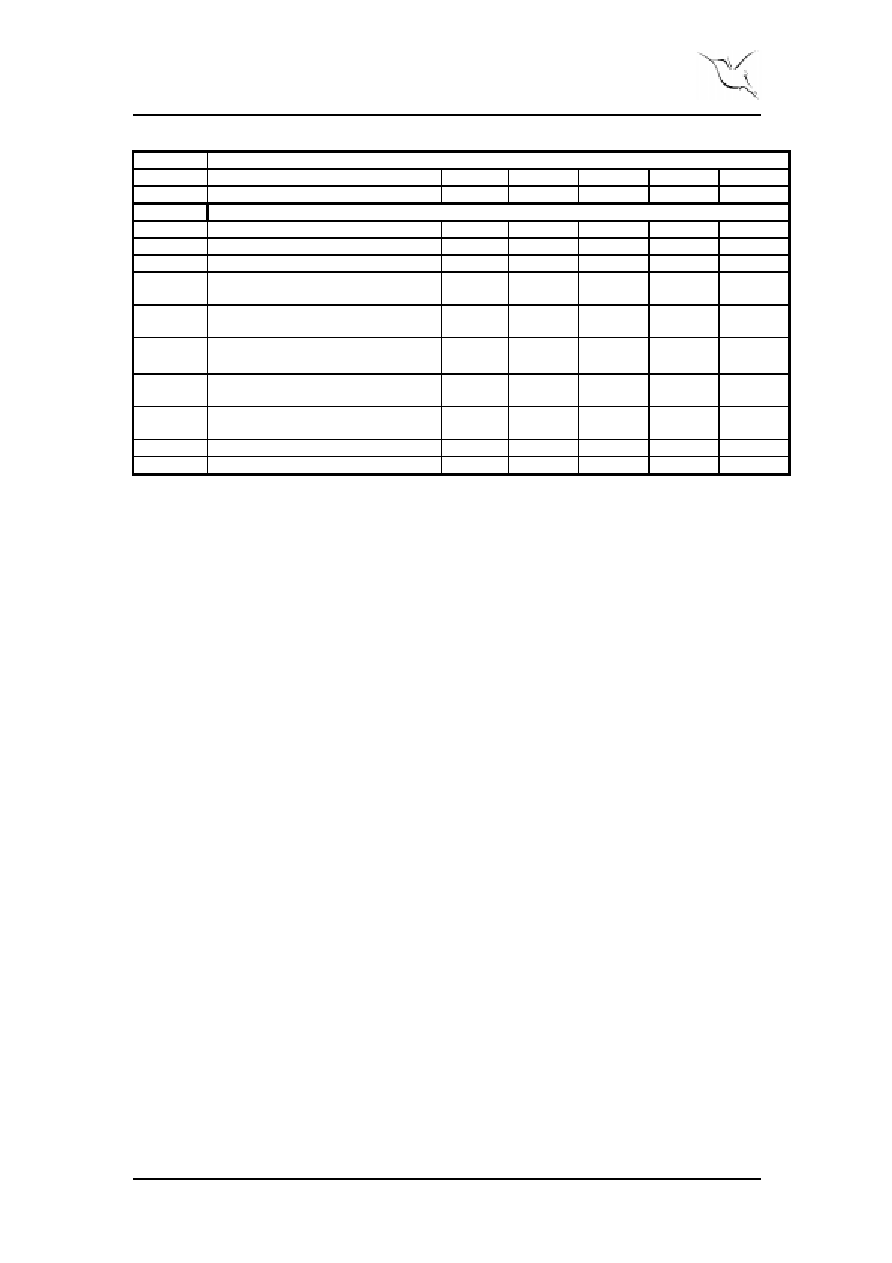
Digital Outputs
V
OL
Logic "0" voltage (I = 2 mA)
IV
0.2
0.4
V
V
OH
Logic "1" voltage (I = 2 mA)
IV
85% OV
DD
90% OV
DD
V
Power Supply
V
DD
Supply voltage
V
1.6
1.8
2.0
V
I
DD
Supply current (except digital output)
IV
mA
V
SS
Supply voltage
GND
P
D
Power dissipation (except digital output)
(10 MSPS)
IV
8
mW
P
D
Power dissipation (except digital output)
(50 MSPS)
IV
33
mW
P
D
Power dissipation (except digital output)
Power Down Mode
2)
IV
45
µW
P
D
Power dissipation (except digital output)
Sleep Mode
IV
655
µW
AV
DD
-
DV
DD1
Analog power ≠ digital power pins
-0.2
+0.2
V
OV
DD
Output driver supply voltage
1.6
1.8
2.0
V
T
Ambient operating temperature
-40
+85
∞
C
Table 2. Electrical specifications
1)
See Figure 5.
2)
Power Down Mode is only available for IP version of nAD1050-18.
Test Levels
Test Level I: 100% production tested at +25∞C
Test Level II: 100% production tested at +25∞C and sample tested at specified
temperatures
Test Level III: Sample tested only
Test Level IV: Parameter is guaranteed by design and characterization testing
Test Level V: Parameter is typical value only
Test Level VI: 100% production tested at +25∞C. Guaranteed by design and
characterization testing for industrial temperature range
ABSOLUTE MAXIMUM RATINGS
Supply voltages
AV
DD
............................- 0.2V to +2.2V
DV
DD1
..................- 0.2V to V
DD
+ 0.2V
OV
DD
...................- 0.2V to V
DD
+ 0.2V
Input voltages
Analog In.......... - 0.2V to AV
DD
+ 0.2V
Digital In..............- 0.2V to V
DD
+ 0.2V
REF
P
................. - 0.2V to AV
DD
+ 0.2V
REF
N
................. - 0.2V to AV
DD
+ 0.2V
CLOCK ...............- 0.2V to V
DD
+ 0.2V
Temperatures
Operating Temperature ....-40 to +85
∞
C
Storage Temperature.. ... - 65 to +125
∞
C
Note: Stress above one or more of the limiting values may cause permanent damage
to the device.
PRODUCT SPECIFICATION
nAD1050-18 10 Bit 50 MSPS Sampling ADC IP
Main office: Nordic VLSI ASA - Vestre Rosten 81, N-7075 Tiller, Norway - Phone +4772898900 - Fax +4772898989
Revision: 3.0
Page 5 of 11
August 31
st
2001
PIN FUNCTIONS
Pin Name
Description
INP INN
Differential input signal pins. Common mode voltage: 0.9V
REFP REFN
Reference input pins. Bypass with 100nF capacitors close to the pins. See Application
Information below.
BIAS0, BIAS1
Digital inputs for max. sampling rate programming.
BIAS1=0, BIAS0=0: Sleep mode (power save)
BIAS1=0, BIAS0=1: - 12.5% bias
BIAS1=1, BIAS0=0: +12.5% bias
BIAS1=1, BIAS0=1: Typ. Bias
The bias setting is automatically performed based on the clock input frequency. This
function should be used ONLY if another bias setting than typical must be used.
CLOCK
Clock input
VCM
Common mode voltage output
BIT9 - BIT0
Digital outputs ( MSB to LSB)
OR
OverRange. High if all outputs are zeros or ones. Available on IP.
OUTEN
Enable digital outputs (Keep low for active outputs)
EXTREF
Disable internal references (Keep low for internal references)
PD
Power Down (Keep low for normal operation) Available on IP or with bonding option.
V
DD
Power pins for on chip power
V
SS
Ground pins
OV
DD
Power pins for output drivers
Table 3. Pin functions
PIN ASSIGNMENT
nAD1050-18
28 PIN SSOP
1
2
3
4
5
6
7
8
9
10
11
12
13
14
BIT9
BIT8
BIT7
BIT6
BIT5
OV
DD
OV
DD
V
SS
V
SS
BIT4
BIT3
BIT2
BIT1
BIT0
28
27
26
25
24
23
22
21
20
19
18
17
16
15
VCM
BIAS1
REFN
REFP
BIAS0
CLOCK
OUTEN
INP
INN
V
DD
V
SS
EXTREF
V
DD
V
SS
Figure 2. Pin assignment for the 28 pin package used for samples
PRODUCT SPECIFICATION
nAD1050-18 10 Bit 50 MSPS Sampling ADC IP
Main office: Nordic VLSI ASA - Vestre Rosten 81, N-7075 Tiller, Norway - Phone +4772898900 - Fax +4772898989
Revision: 3.0
Page 6 of 11
August 31
st
2001
IP BLOCK LAYOUT
REFP
REFN
BIAS1
BIAS0
EXT
R
E
F
VC
M
IN
P
IN
N
CLOCK
OR
BIT
9
:
BIT
0
AVSS
AVDD
AVSS
AVDD
VDD
X
Y
AVSS
AVDD
AVSS
AVDD
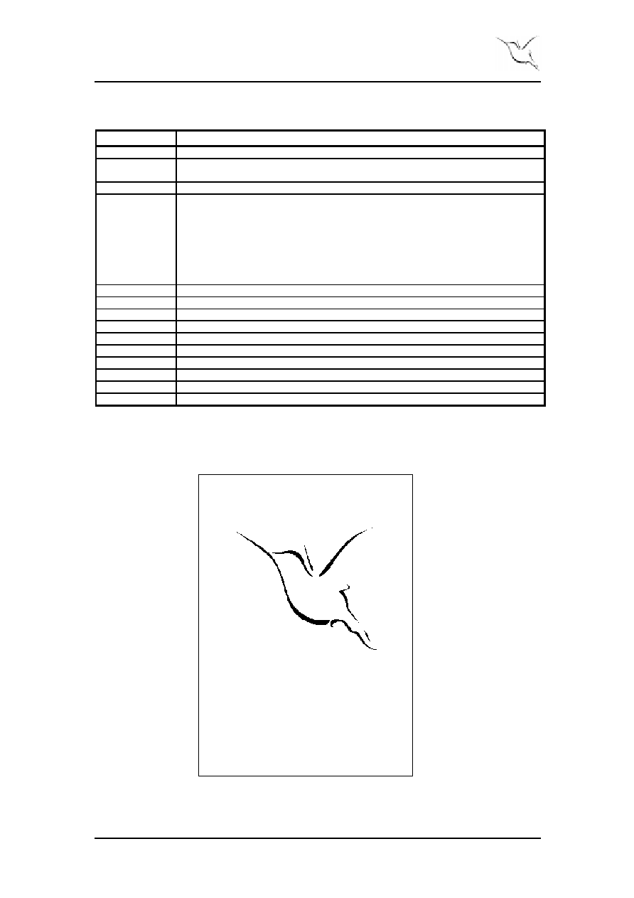
Figure 3. Size and pin placement for nAD1050-18.
The height and width of the layout is X =1208
µ
m and Y=711
µ
m respectively in the
0.18
µ
m CMOS process.
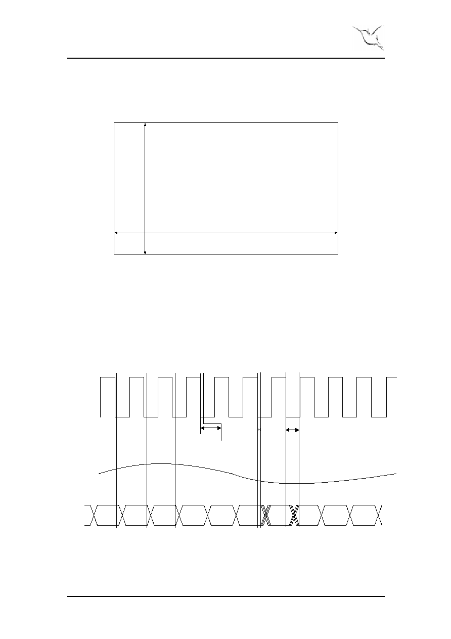
TIMING DIAGRAM
Figure 4. Timing diagram
DATA
CLOCK
S
A
M
N - 1
P
L
E
S
A
M
N + 1
P
L
E
S
A
M
N
P
L
E
Data
N
Data
N-1
Data
N+1
t
d
t
AP
S
A
M N + 2
P
L
E
t
h
PRODUCT SPECIFICATION
nAD1050-18 10 Bit 50 MSPS Sampling ADC IP
Main office: Nordic VLSI ASA - Vestre Rosten 81, N-7075 Tiller, Norway - Phone +4772898900 - Fax +4772898989
Revision: 3.0
Page 7 of 11
August 31
st
2001
INPUT SIGNAL RANGE
Figure 5. Definition of full scale range
DEFINITIONS
Data sheet status
Objective product specification
This datasheet contains target specifications for product development.
Preliminary product
specification
This datasheet contains preliminary data; supplementary data may be
published from Nordic VLSI ASA later.
Product specification
This datasheet contains final product specifications.
Limiting values
Stress above one or more of the limiting values may cause permanent damage to the device. These are stress
ratings only and operation of the device at these or at any other conditions above those given in the
Specifications sections of the specification is not implied. Exposure to limiting values for extended periods may
affect device reliability.
Application information
Where application information is given, it is advisory and does not form part of the specification.
Table 4. Definitions
LIFE SUPPORT APPLICATIONS
These products are not designed for use in life support appliances, devices, or systems
where malfunction of these products can reasonably be expected to result in personal
injury. Nordic VLSI ASA customers using or selling these products for use in such
applications do so at their own risk and agree fully indemnify Nordic VLSI ASA for
any damages resulting from such improper use or sale.
V
REFP
V
REFN
V
CM
V
INP
V
INN
V
INP
-V
INN
V
RR
+V
RR
-V
RR
V
FSR
PRODUCT SPECIFICATION
nAD1050-18 10 Bit 50 MSPS Sampling ADC IP
Main office: Nordic VLSI ASA - Vestre Rosten 81, N-7075 Tiller, Norway - Phone +4772898900 - Fax +4772898989
Revision: 3.0
Page 8 of 11
August 31
st
2001
APPLICATION INFORMATION
References
The nAD1050-18 has a differential analog input. The input range is determined by the
voltages V
REFP
and V
REFN
applied to reference pins REFP and REFN respectively, and
is equal to
±
(V
REFP
-V
REFN
). Externally generated reference voltages connected to
REFP and REFN should be symmetrical around 0.9V. The input range can be defined
between
±
0.5V and
±
0.75V. The references should be bypassed as close to the
converter pins as possible using 100nF capacitors in parallel with smaller capacitors
(e.g. 1nF) (to ground).
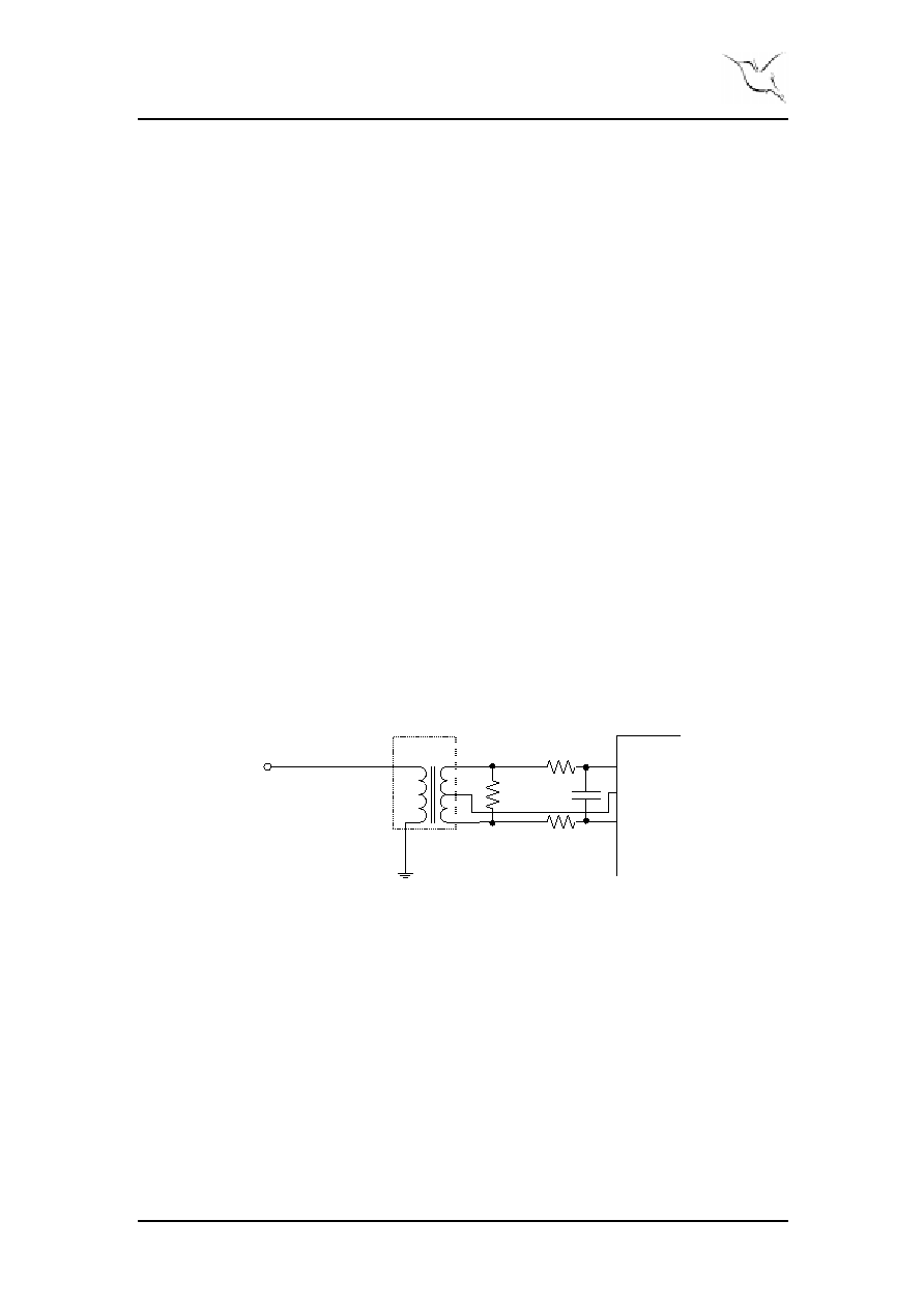
Analog input
The input of the nAD1050-18 can be configured in various ways - dependent upon
whether a single ended or differential, AC- or DC-coupled input is wanted.
AC-coupled input is most conveniently implemented using a transformer with a center
tapped secondary winding. The center tap is connected to the CM-node, as shown in
figure 6. In order to obtain low distortion, it is important that the selected transformer
does not exhibit core saturation at full-scale. Excellent results are obtained with the
Mini Circuits T1-6T or T1-1T. Proper termination of the input is important for input
signal purity. A small capacitor across the inputs attenuates kickback-noise from the
sample and hold. Series resistors as shown in Figure 6 may be advantageous to
improve linearity. The VCM-node should be bypassed to ground as closed to the
converter pin as possible using 100nF capacitors in parallel with a small one.
INP
INN
VCM
Mini Circuits
T1-6T
V
in
ADC
51
50
50
22pF
Figure 6. Example of AC coupled input using transformer configuration
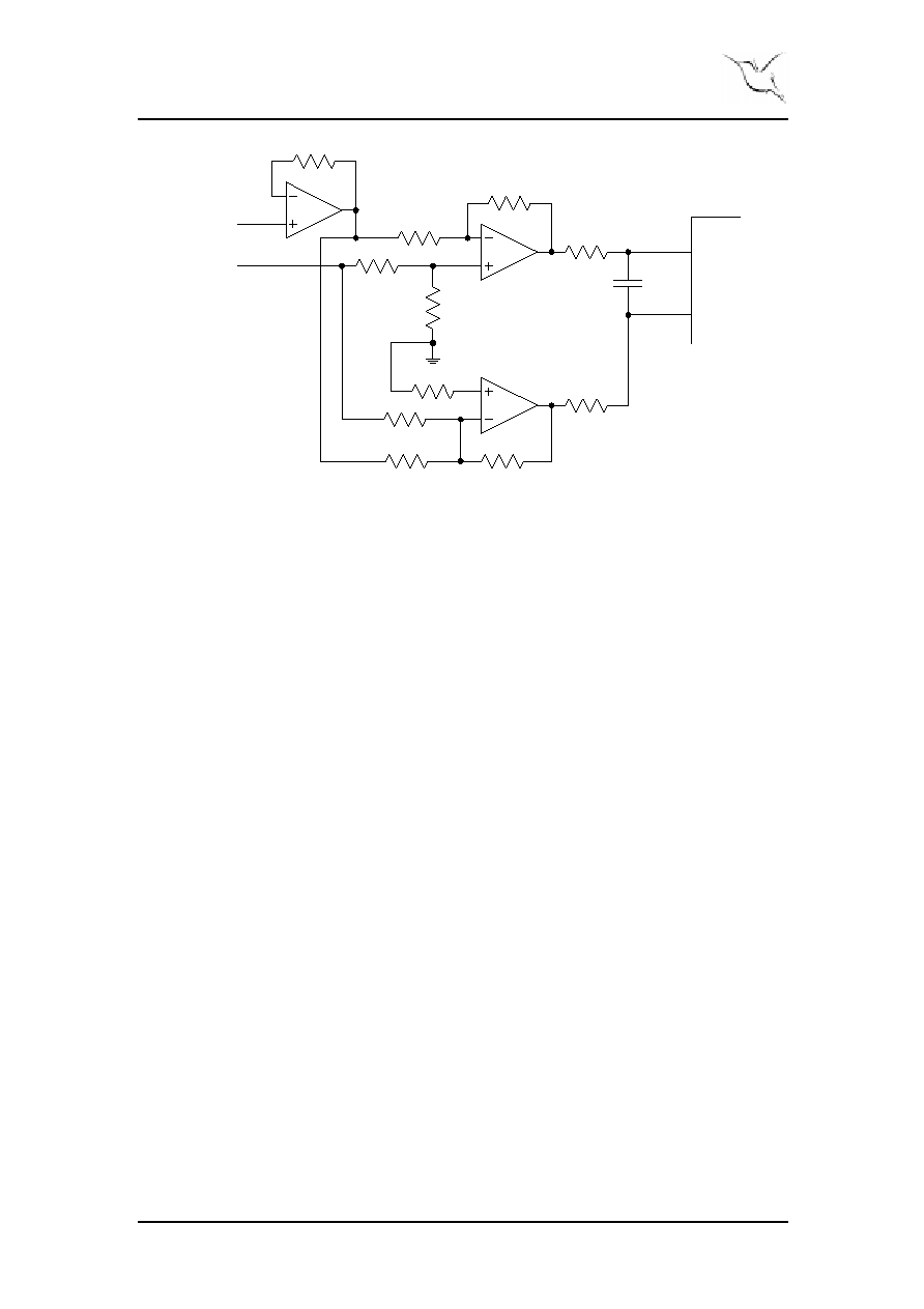
If a DC-coupled single ended input is wanted, a solution based on operational
amplifiers - as shown in Figure 7, is usually preferred. The AD826 is suggested for
low distortion and video bandwidth. Lower cost operational amplifiers may be used if
the demands are less strict. A good alternative for high performance applications is to
use AD8138 single ended to differential amplifier.
PRODUCT SPECIFICATION
nAD1050-18 10 Bit 50 MSPS Sampling ADC IP
Main office: Nordic VLSI ASA - Vestre Rosten 81, N-7075 Tiller, Norway - Phone +4772898900 - Fax +4772898989
Revision: 3.0
Page 9 of 11
August 31
st
2001
AD826
AD826
51
51
470
470
100
100
470
470
AD826
51
IN
P
IN
N
51
470
Input
offset
Video
in
ADC
15pF
Figure 7. DC-coupled single ended to differential conversion (power supplies and
bypassing not shown)
Clock
In order to preserve accuracy at high input frequency, it is important that the clock has
low jitter and steep edges. Rise/fall times should be kept shorter than 2ns whenever
possible. Overshoot should be avoided. Low jitter is especially important when
converting high frequency input signals. Jitter causes the noise floor to rise
proportionally to input signal frequency. Jitter may be caused by crosstalk on the PCB.
It is therefore recommended that the clock trace on the PCB is made as short as
possible.
Digital outputs
The digital output data appears in offset binary code at CMOS logic levels. Full-scale
negative input results in output code 000...0. Full-scale positive input results in output
code 111...1. Output data are available 6 clock cycles after the data are sampled. The
analog input is sampled one aperture delay (t
AP
) after the high to low clock transition.
Output data should be sampled as shown in the timing diagram.
PCB layout and decoupling
A well designed PCB is necessary to get good spectral purity from any high
performance ADC. A multilayer PCB with a solid ground plane is recommended for
optimum performance. If the system has a split analog and digital ground plane, it is
recommended that all ground pins on the ADC are connected to the analog ground
plane. It is our experience that this gives the best performance. The power supply pins
should be bypassed using 100nF surface mounted capacitors as close to the package
pins as possible. Analog and digital supply pins should be separately filtered.

PRODUCT SPECIFICATION
nAD1050-18 10 Bit 50 MSPS Sampling ADC IP
Main office: Nordic VLSI ASA - Vestre Rosten 81, N-7075 Tiller, Norway - Phone +4772898900 - Fax +4772898989
Revision: 3.0
Page 10 of 11
August 31
st
2001
Dynamic testing
Careful testing using high quality instrumentation is necessary to achieve accurate test
results on high speed A/D-converters. It is important that the clock source and signal
source has low jitter. A spectrally pure, low noise RF signal generator - such as the
HP8662A or HP8644B is recommended for the test signal. Low pass filtering or band
pass filtering of the input signal is usually necessary to obtain the required spectral
purity (SFDR > 75dB). The clock signal can be obtained from either a crystal
oscillator or a low-jitter pulse generator. Alternatively, a low-jitter RF-generator can
be used as a clock source. At Nordic VLSI, the Marconi Instruments 2041A is used.
The sinewave clock must then be applied to an ultra high-speed comparator (e.g.
AD9696) and a TTL to CMOS level shifter (e.g. 74LV04) before application to the
converter. The most consistent results are obtained if the clock signal is phase locked
to the input signal. Phase locking allows testing without windowing of output data. A
logic analyzer with deep memory - such as the HP16500-series, is recommended for
test data acquisition.
Power Down Mode and Sleep Mode
The nAD1050-18 has both Power Down Mode and Sleep Mode. The Power Down
Mode can be used when the ADC should be put to `zero current consumption' state
and when a somewhat longer startup time is allowed. The Sleep Mode can be used to
put the ADC in an `idle' state and when the application require a quick startup. The
two different power consumption saving schemes can be activated through the PD,
BIAS0 and BIAS1 pins/connections in the following manner:
Power Down Mode: PD=1, BIAS0=0, BIAS1=0
Sleep Mode: PD=0, BIAS0=0, BIAS1=0
The actual startup time from these modes are dependent on the external decopling
configuration.
PRODUCT SPECIFICATION
nAD1050-18 10 Bit 50 MSPS Sampling ADC IP
Main office: Nordic VLSI ASA - Vestre Rosten 81, N-7075 Tiller, Norway - Phone +4772898900 - Fax +4772898989
Revision: 3.0
Page 11 of 11
August 31
st
2001
DESIGN CENTER
Nordic VLSI ASA
Vestre Rosten 81
N-7075 TILLER
NORWAY
Telephone:
+47 72898900
Telefax:
+47 72898989
E-mail: For further information regarding our state of the art data converters, please e-
mail us at datacon@nvlsi.no.
World Wide Web/Internet: Visit our site at http://www.nvlsi.no.
ORDERING INFORMATION
Type number
Description
Price
nAD1050-18-IC
nAD1050-18 sample in SSOP28 package
(limited availability)
USD 50
nAD1050-18-EVB
nAD1050-18 evaluation board including
characterisation report and user guide
USD 300
Table 5. Ordering information
Product Specification. Revision Date: August 31
st
, 2001
All rights reserved Æ. Reproduction in whole or in part is prohibited without the prior
written permission of the copyright holder. Company and product names referred to in
this datasheet belong to their respective copyright/trademark holders.