PRELIMINARY PRODUCT SPECIFICATION
Main office: Nordic VLSI ASA - Vestre Rosten 81, N-7075 Tiller, Norway - Phone +4772898900 - Fax +4772898989
Revision: 2.0
Page 1 of 10
December 13
th
2002
12-Bit 80MSPS 0.18
µ
m
Analog-to-Digital Converter IP
FEATURES
∑
1.8V power supply
∑
SNR typ 65dB for (f
in
= 10MHz)
∑
Low power (75mW @ 1.8V and
80MSPS)
∑
Compact area (0.86mm
2
)
∑
Frequency dependent biasing
∑
Differential input
∑
Low input capacitance
∑
Three power saving idle modes
APPLICATIONS
∑
Imaging
∑
Wireless communication
∑
WLAN/IEEE 802.11x
∑
DVB receivers
∑
Powerline communication
∑
Video products
GENERAL DESCRIPTION
The nAD1280-18 is a compact, high-speed, low power 12-bit monolithic analog-to-
digital converter, implemented in the TSMC logic 0.18
µ
m CMOS process. No mixed
mode process options are needed. The converter includes a high bandwidth sample
and hold. Using internal references, the full scale range is
±
0.75V. The full scale range
can be set between
±
0.5V and
±
0.75V using external references. It operates from a
single 1.8V supply. Its low distortion and high dynamic range offers the performance
needed for demanding imaging, multimedia, telecommunications and instrumentation
applications. The bias current level for the ADC is automatically adjusted based on
the clock input frequency. Hence, the power dissipation of the device is continuously
minimised for the current operation frequency.
The nAD1280-18 has a pipelined architecture - resulting in low input capacitance.
Digital error correction of the 11 most significant bits ensures good linearity for input
frequencies approaching Nyquist. The nAD1280-18 is compact. The core occupies
0.86mm
2
of die area. The fully differential architecture makes it insensitive to
substrate noise. Thus it is ideal as a mixed mode IP in a SoC design.
QUICK REFERENCE DATA
Symbol
Parameter
Conditions
Min.
Typ.
Max.
Unit
V
DD
Supply voltage
1.6
1.8
2.0
V
P
D
Power dissipation
(80 MSPS)
Except digital
output drivers
75
mW
DNL
Differential nonlinearity
f
IN
=0.9991MHz
±0.5
LSB
INL
Integral nonlinearity
f
IN
=0.9991MHz
±
1.5
LSB
SNR
Signal to noise ratio
f
IN
=10MHz
62
65
dB
SFDR
Spurious free dynamic
range
f
IN
=10MHz
70
dB
Table 1: Quick reference data
nAD1280-18
PRELIMINARY PRODUCT SPECIFICATION
nAD1280-18: 12 Bit 80 MSPS 0.18
µ
m ADC IP
Main office: Nordic VLSI ASA - Vestre Rosten 81, N-7075 Tiller, Norway - Phone +4772898900 - Fax +4772898989
Revision: 2.0
Page 2 of 10
December 13
th
2002
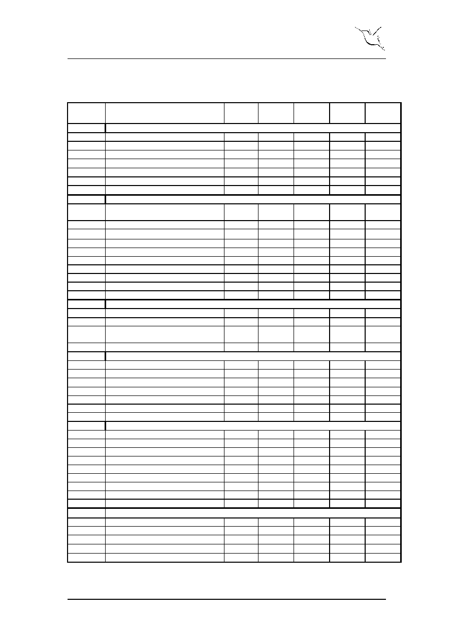
ELECTRICAL SPECIFICATIONS
(
At T
A
= 25
∞
C, V
DD
= 1.8V, Sampling Rate = 80MHz, Input frequency = 10MHz, Differential input
signal, 50% duty cycle clock and 300nF Reference decoupling unless otherwise noted
)
Symbol Parameter (condition)
Test
Level
Min.
Typ.
Max.
Units
DC Accuracy
DNL
Differential Nonlinearity
f
IN
= 0.9991 MHz
IV
±
0.5
LSB
INL
Integral Nonlinearity
f
IN
= 0.9991 MHz
IV
±
1.5
LSB
V
OS
Midscale offset
±
1
%FS
CMRR
Common Mode Rejection Ratio
-59
dB
G
Gain Error
±
1
%FS
Dynamic Performance
SNR
Signal to Noise Ratio (without
harmonics)
f
IN
= 10 MHz
IV
62
65
dBFS
f
IN
= 40 MHz
1)
IV
60
63
dBFS
f
IN
= 72 MHz
1)
IV
56
60
dBFS
SINAD
Signal to Noise and Distortion Ratio
f
IN
= 10 MHz
IV
64
dBFS
SFDR
Spurious Free Dynamic Range
f
IN
= 10 MHz
IV
70
dB
f
IN
= 40 MHz
IV
63
dB
f
IN
= 72 MHz
IV
50
dB
Analog Input
V
FSR
Input Voltage Range (differential)
IV
±
0.75
V
V
CMI
Analog input common mode voltage
IV
0.8
0.9
1.0
V
C
INA
Input Capacitance (from each input to
ground)
2.2
pF
Input signal attenuation @ 70MHz
0.35
dB
Reference Voltages
V
REF0
Internal reference voltage on pin 10
IV
0.525
V
V
REF1
Internal reference voltage on pin 11
IV
1.275
V
Internal reference voltage drift
100
ppm/
∞
C
V
REF0
Negative Input Voltage (external ref)
IV
0.525
V
V
REF1
Positive Input Voltage (external ref)
IV
1.275
V
V
RR
Reference input voltage range
2)
IV
0.75
V
V
CM
Common mode voltage output
IV
0.9
V
Switching Performance
F
S max
Maximum Conversion Rate
IV
80
105
MSPS
F
S min
Minimum Conversion Rate
10
15
MSPS
Pipeline Delay
IV
7
Clocks
t
AP
Aperture delay, IP
V
0.9
ns
t
h
Output hold time, IP (0.1 ≠ 0.8 pF load)
V
1
ns
t
d
Output delay time, IP (0.1 - 0.8 pF load)
V
2
ns
t
AP
Aperture delay, with bonding pad
V
1.0
ns
t
h
Output hold time, with bonding pad
V
1.0
ns
t
d
Output delay time, with bonding pad
V
4.0
ns
Digital Inputs
V
IL
Logic "0" voltage
IV
0.4
V
V
IH
Logic "1" voltage
IV
AV
DD
≠0.4
V
I
IL
Logic "0" current (V
I
=V
SS
)
IV
±
10
µ
A
I
IH
Logic "1" current (V
I
=V
DD
)
IV
±
10
µ
A
C
IND
Input Capacitance
IV
0.03
0.1
pF
(table continued on next page)
1)
Requires 1ps clock source jitter, and 1.5ps total on-chip jitter.
2)
See Figure 5.
PRELIMINARY PRODUCT SPECIFICATION
nAD1280-18: 12 Bit 80 MSPS 0.18
µ
m ADC IP
Main office: Nordic VLSI ASA - Vestre Rosten 81, N-7075 Tiller, Norway - Phone +4772898900 - Fax +4772898989
Revision: 2.0
Page 3 of 10
December 13
th
2002
Digital Outputs
V
OL
Logic "0" voltage (I = 2 mA)
IV
0.2
0.4
V
V
OH
Logic "1" voltage (I = 2 mA)
IV
85% OV
DD
90% OV
DD
V
Power Supply
V
DD
Supply voltage
V
1.6
1.8
2.0
V
I
DD
Supply current (except digital output)
IV
27.8
mA
V
SS
Supply voltage
GND
P
D
Power dissipation (except digital output)
(active 10 MSPS)
IV
12
mW
P
D
Power dissipation (except digital output)
(active 80 MSPS)
IV
75
mW
P
D
Power dissipation (except digital output)
Power Down Mode
IV
70
µW
P
D
Power dissipation (except digital output)
Sleep Mode
IV
3
mW
P
D
Power dissipation (except digital output)
Standby Mode
IV
12
mW
t
start
Start-up time from Power down
1.3
ms
t
start
Start-up time from Sleep mode
2
µ
s
t
start
Start-up time from Stand By
8
clock cycles
OV
DD
Output driver supply voltage
1.6
1.8
3.6
V
T
Junction operating temperature
-40
+125
∞
C
Table 2: Electrical specifications
Test Levels
Test Level I: 100% production tested at +25∞C
Test Level II: 100% production tested at +25∞C and sample tested at specified
temperatures
Test Level III: Sample tested only
Test Level IV: Parameter is guaranteed by design and characterization testing
Test Level V: Parameter is typical value only
Test Level VI: 100% production tested at +25∞C. Guaranteed by design and
characterization testing for industrial temperature range
ABSOLUTE MAXIMUM RATINGS
Supply voltages
V
DD
............................... - 0.2V to +2.2V
OV
DD
.............................. - 0.2V to 3.6V
Input voltages
Analog In ............ - 0.2V to V
DD
+ 0.2V
Digital In ........................ - 0.2V to 3.6V
REF
P
.................... - 0.2V to V
DD
+ 0.2V
REF
N
................... - 0.2V to V
DD
+ 0.2V
CLOCK.......................... - 0.2V to 3.6V
Temperatures
Operating Temperature....-40 to +125
∞
C
Storage Temperature.. - 65 to +125
∞
C
Note: Stress above one or more of the limiting values may cause permanent damage
to the device.
PRELIMINARY PRODUCT SPECIFICATION
nAD1280-18: 12 Bit 80 MSPS 0.18
µ
m ADC IP
Main office: Nordic VLSI ASA - Vestre Rosten 81, N-7075 Tiller, Norway - Phone +4772898900 - Fax +4772898989
Revision: 2.0
Page 4 of 10
December 13
th
2002
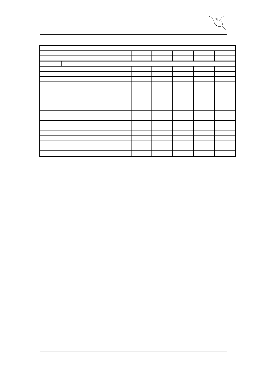
PIN FUNCTIONS
Table 3: Pin functions
IP BLOCK LAYOUT
Figure 1: IP-footprint for nAD1280-18
Pin Name
Description
X
Y
Metal layer
INN
Differential input signal.
40
651.5
2
VCM
Common mode voltage
42
651.5
2
INP
Differential input signal.
44
651.5
2
AVDD
Analog power
0-35,50-1312
651.5
2
AVSS
Analog and digital ground
0-35,50-1312
651.5
3
REF[1]
Reference pin
1312.5
550
5
REF[0]
Reference pin
1312.5
540
5
VDD
Digital power
1312.5
280
4
EXTREF
Disables internal voltage references when high. External
voltages must be applied to REF[1:0]
1249.8
0.5
2
BCTRL[2]
Power consumption scaling
1249.0
0.5
2
BCTRL[1]
Power consumption scaling
1248.2
0.5
2
BCTRL[0]
Power consumption scaling
1247.4
0.5
2
PD
Power down
1246.6
0.5
2
STBY
Standby mode
1245.8
0.5
2
AVDD
Analog power
0-1200
0.5
2
AVSS
Analog and digital ground
0-1200
0.5
3
OR
Over-range Flag
0
285.5
2
BITO[0]
Output bit
0
289.5
2
BITO[1]
Output bit
0
290.5
2
BITO[2]
Output bit
0
291.5
2
BITO[3]
Output bit
0
292.5
2
BITO[4]
Output bit
0
293.5
2
BITO[5]
Output bit
0
294.5
2
BITO[6]
Output bit
0
295.5
2
BITO[7]
Output bit
0
296.6
2
BITO[8]
Output bit
0
297.5
2
BITO[9]
Output bit
0
298.5
2
BITO[10]
Output bit
0
299.5
2
BITO[11]
Output bit
0
300.5
2
VDD
Digital power
0
304
4
CLK
ADC clock
0
317
2
IP_footprint
REF[1:0]
V
C
M
I
N
P
I
N
N
CLK
OR
BITO[11:0]
A
V
S
S
A
V
D
D
A
V
S
S
A
V
D
D
VDD
Y
=
6
5
2
u
m
VDD
X=1313um
B
C
T
R
L
[
2
:
0
]
E
X
T
R
E
F
O
P
M
[
1
:
0
]
PRELIMINARY PRODUCT SPECIFICATION
nAD1280-18: 12 Bit 80 MSPS 0.18
µ
m ADC IP
Main office: Nordic VLSI ASA - Vestre Rosten 81, N-7075 Tiller, Norway - Phone +4772898900 - Fax +4772898989
Revision: 2.0
Page 5 of 10
December 13
th
2002
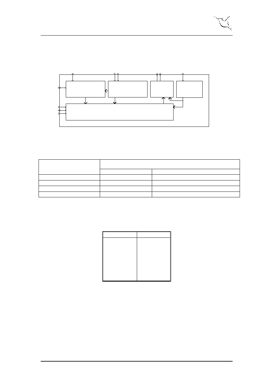
FUNCTIONAL BLOCK DIAGRAM
Figure 2: Functional Block diagram nAD1280-18
MODES OF OPERATION
The ADC has four different modes of operation, controlled as described in Table 4:
OPM control settings
Mode of operation
OPM[1]
OPM[0]
Active
HIGH
HIGH
Standby
HIGH
LOW
Sleep
LOW
HIGH
Power down
LOW
LOW
Table 4: Control settings for ADC operational modes
Active mode
In the active mode, the ADC is fully functional.
The current consumption can be adjusted with the BCTRL[2:0] bus:
BCTRL[2:0]
CURRENT
000
Typical*3/7
001
Typical*4/7
010
Typical*5/7
011
Typical*6/7
100
Typical
101
Typical*8/7
110
Typical*9/7
111
Typical*10/7
Idle modes
In the three idle modes, the ADC is not functional. The different modes are
distinguished primary by power consumption and start-up time. Start-up time is
defined as the time it takes for the ADC to reach full performance in active mode
when switched from an idle mode. Refer to `Electrical Specifications' for power
consumption and start-up times for the different modes.
While the start-up times for standby and sleep modes are constant, the start-up time in
power down mode will be proportional to Off-Chip REF[1:0] decoupling. The amount
of decoupling on the REF[1:0] will have impact on the performance.
CURRENT
BIAS
VOLTAGE
REFERENCE
DIGITAL
CLOCK
DRIVER
PIPELINE CHAIN
INN
INP
REF[1:0]
E
X
T
R
E
F
O
P
M
[
1
:
0
]
B
C
T
R
L
[
2
:
0
]
C
L
K
B
I
T
O
[
1
1
:
0
]
O
R
VCM