PRELIMINARY PRODUCT SPECIFICATION
Main office: Nordic VLSI ASA - Vestre Rosten 81, N-7075 Tiller, Norway - Phone +4772898900 - Fax +4772898989
Revision: 1.0
Page 1 of 7
May 7
th
2002
12-Bit 80MSPS 0.18
µ
m
Analog-to-Digital Converter IP
FEATURES
∑
3.3V power supply
∑
150
µ
V input referred noise
∑
Low power (250mW @ 3.3V and
80MSPS)
∑
Compact area (2.47mm
2
)
∑
Frequency dependent biasing
∑
Single ended input
∑
1X-2X gain input stage
∑
Low input capacitance
∑
Two power saving idle modes
∑
TSMC Imaging process: 4 metal
layers
GENERAL DESCRIPTION
The nAD1280-18TS is a compact, high-speed, low power 12-bit monolithic analog-
to-digital converter, implemented in the TSMC imaging 0.18
µ
m CMOS process with
MiM capacitor and thick oxide options, and 4 metal layers. The converter includes a
single ended to differential low-noise input stage, with 1X or 2X gain, making it ideal
for imaging applications. Using internal references, the full scale range is 0-1V in 2X
mode and 0-2V in 1X mode. The full scale range can be reduced by using external
references. It operates from a single 3.3V supply. The bias current level for the ADC
is automatically adjusted based on the clock input frequency. Hence, the power
dissipation of the device is continuously minimised for the current operation
frequency.
The nAD1280-18TS has a pipelined architecture - resulting in low input capacitance.
Digital error correction of the 11 most significant bits ensures good linearity for input
frequencies approaching Nyquist. The nAD1280-18TS is compact. The core occupies
less than 2.5mm
2
of die. The differential architecture makes it insensitive to substrate
noise. Thus it is ideal as a mixed signal ASIC macro cell.
QUICK REFERENCE DATA
Symbol
Parameter
Conditions
Min.
Typ.
Max.
Unit
V
DD
Supply voltage
2.95
3.3
3.6
V
P
D
Power dissipation
80MSPS
250
mW
DNL
Differential nonlinearity
f
IN
=0.9991MHz
±0.5
LSB
INL
Integral nonlinearity
f
IN
=0.9991MHz
TBD
LSB
Vnrms
Input referred noise
1X-mode
250
400
µ
V
Vnrms
Input referred noise
2X-mode
150
200
µ
V
Table 1: Quick reference data
nAD1280-18TS
PRODUCT SPECIFICATION
nAD1280-18TS: 12 Bit 80 MSPS 0.18
µ
m 3.3V ADC IP
Main office: Nordic VLSI ASA - Vestre Rosten 81, N-7075 Tiller, Norway - Phone +4772898900 - Fax +4772898989
Revision: 1.0
Page 2 of 7
May 7
th
2002
ELECTRICAL SPECIFICATIONS
(
At T
A
= 25
∞
C, V
DD
= 3.3V, Sampling Rate = 80MHz, Input frequency = 10MHz, Differential input
signal, 50% duty cycle clock and 300nF Reference decoupling unless otherwise noted
)
Symbol Parameter (condition)
TestLev.
Min.
Typ.
Max.
Units
DC Accuracy
DNL
Differential Nonlinearity
f
IN
= 0.9991 MHz
±
0.5
LSB
INL
Differential Nonlinearity
f
IN
= 0.9991 MHz
TBD
LSB
V
OS
Midscale offset
±
1
%FS
G
Gain Error
±
2
%FS
Dynamic Performance
Vnrms
Input referred noise (1X-mode)
250
400
µ
V
Vnrms
Input referred noise (2X mode)
150
200
µ
V
Analog Input
V
FSR
Input Voltage Range (1X-mode)
2
V
V
FSR
Input Voltage Range (2X-mode)
1
V
C
INA
Input Capacitance (1X-mode)
1.8
pF
C
INA
Input Capacitance (1X-mode)
3.5
pF
Input signal attenuation
TBD
dB
Reference Voltages
V
REF[0]
Internal reference voltage on ref[0]
1.15
V
V
REF[1]
Internal reference voltage on ref[1]
2.15
V
Internal reference voltage drift
100
ppm/
∞
C
V
REF[0]
Negative Input Voltage (external ref)
1.15
V
V
REF[1]
Positive Input Voltage (external ref)
2.15
V
V
RR
Reference input voltage range
1
V
Switching Performance
F
S max
Maximum Conversion Rate
80
MSPS
F
S min
Minimum Conversion Rate
15
MSPS
Pipeline Delay
7
Clocks
t
AP
Aperture delay, IP
0.7
1
1.5
ns
t
h
Output hold time, IP (max 0.2 pF load)
1.5
2
3.5
ns
t
d
Output delay time, IP (max 0.2 pF load)
2
3
4.5
ns
Digital Inputs
V
IL
Logic "0" voltage
0.25
V
V
IH
Logic "1" voltage
AV
DD
≠0.25
V
I
IL
Logic "0" current (V
I
=V
SS
)
±
10
µ
A
I
IH
Logic "1" current (V
I
=V
DD
)
±
10
µ
A
C
IND
Input Capacitance
0.03
0.1
pF
Digital Outputs
V
OL
Logic "0" voltage (I = 2 mA)
0.1
0.25
V
V
OH
Logic "1" voltage (I = 2 mA)
85% OV
DD
90% OV
DD
V
Power Supply
V
DD
Supply voltage
3.0
3.3
3.6
V
I
DD
Supply current (except digital output)
755
mA
V
SS
Supply voltage
GND
P
D
Power dissipation active 15 MSPS
TBD
mW
P
D
Power dissipation active 80 MSPS
250
mW
P
D
Power dissipation Power Down Mode
TBD
µW
P
D
Power dissipation Standby Mode
TBD
mW
t
start
Start-up time from Power down
TBD
ms
t
start
Start-up time from Stand By
TBD
clock cycles
T
Junction operating temperature
-40
+125
∞
C
Table 2: Electrical specifications
PRODUCT SPECIFICATION
nAD1280-18TS: 12 Bit 80 MSPS 0.18
µ
m 3.3V ADC IP
Main office: Nordic VLSI ASA - Vestre Rosten 81, N-7075 Tiller, Norway - Phone +4772898900 - Fax +4772898989
Revision: 1.0
Page 3 of 7
May 7
th
2002
PIN FUNCTIONS AND PLACEMENT
Signals
Pads
Functions
X-coordinate
Y-coordinate
Metal-layer
GAIN_CTRL
1
1X/2X gain setting
337
1466
2
BITO(11:0)
12
Output bits
854,829,804,779,
755,230,705,680,
655,630,605,580
1466
2
OR_FLAG
1
Overflow-flag
880
1466
2
CLK
1
Clock
904
1466
2
REF_SEL
1
Disabling internal references
920
1466
2
PDBUS(2:0)
3
Powerdown control
952,944,936
1466
2
BSC(1:0)
1
Bias current control
969,984
1466
2
VDD_DIG
1
Digital power
1661-1683
0
2,3,Top
REF(1:0)
2
Reference voltages
1595,1572
0
3
AVSS
2
Common ground
875-1525
0
3,Top
AVDD
2
Analog ground
0-870
0
3,Top
IN_REF
1
Negative input
56
0
2
IN
1
Input signal
50
0
2
Table 3: Pin functions and placement
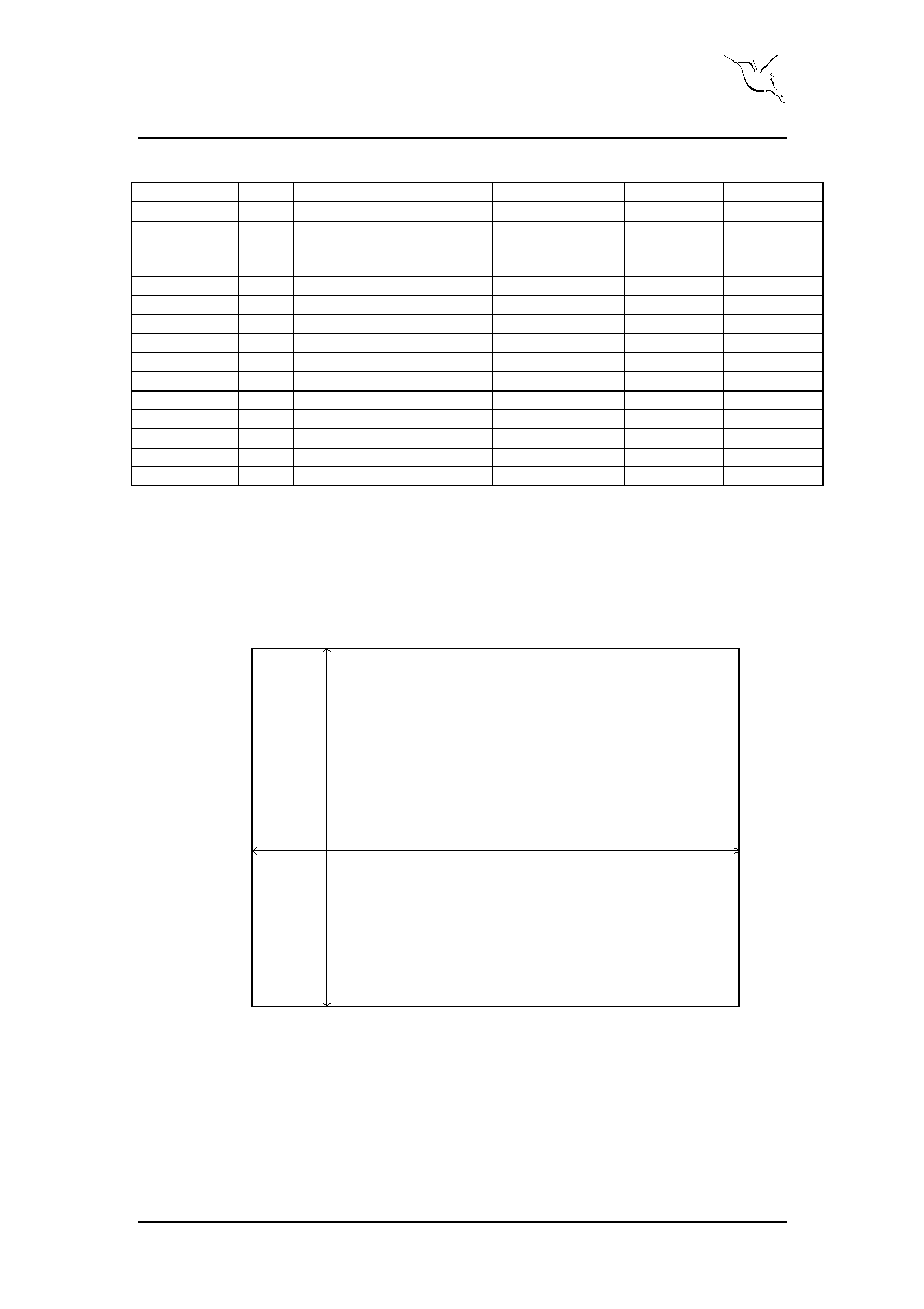
IP BLOCK LAYOUT
Figure 1: Size and pin placement for nAD1280-18TS IP
Y
=
1
4
6
6
u
m
X=1684um
C
L
K
G
A
I
N
_
C
T
R
L
B
S
C
(
1
:
0
)
R
E
F
_
S
E
L
O
R
_
F
L
A
G
AVDD
V
D
D
_
D
I
G
P
D
B
U
S
(
2
:
0
)
IP_nAD1280-18TS
AVSS
I
N
I
N
_
R
E
F
B
I
T
O
(
1
1
:
0
)
R
E
F
(
1
:
0
)

PRODUCT SPECIFICATION
nAD1280-18TS: 12 Bit 80 MSPS 0.18
µ
m 3.3V ADC IP
Main office: Nordic VLSI ASA - Vestre Rosten 81, N-7075 Tiller, Norway - Phone +4772898900 - Fax +4772898989
Revision: 1.0
Page 4 of 7
May 7
th
2002
FUNCTIONAL BLOCK DIAGRAM
Figure 2: Functional Block diagram nAD1280-18TS
MODES OF OPERATION
The ADC has four different modes of operation, controlled as described in Table 4:
Digital control and clock settings
Mode of operation
BSC(1:0)
PDBUS(2:0)
CLOCK
Active
HIGH,HIGH
LOW,LOW,LOW
Running
Standby
LOW,LOW
HIGH,LOW,HIGH
Running
Power down
LOW,LOW
HIGH,HIGH,HIGH
Stopped
Table 4: Control settings for ADC operational modes
Active mode
In the active mode, the ADC is fully functional.
A performance versus power consumption trade off can be made by adding or
subtracting 12.5% of the pipeline bias current with the bias1 and bias0 pins:
BSC(1:0)
CURRENT
01
-12.5%
10
+12.5%
11
Typical
Idle modes
In the two idle modes, the ADC is not functional. The different modes are
distinguished primary by power consumption and start-up time. Start-up time is
defined as the time it takes for the ADC to reach full performance in active mode
REF(1:0)
REF_SEL
nAD1280_18T
S2D
B
S
C
(
1
:
0
)
ADC_INP
ADC_INN
C
L
K
O
R
_
F
L
A
G
B
I
T
O
(
1
1
:
0
)
IN
IN_REF
nAD1280S
P
D
B
U
S
(
2
:
0
)
G
A
I
N
_
C
T
R
L

PRODUCT SPECIFICATION
nAD1280-18TS: 12 Bit 80 MSPS 0.18
µ
m 3.3V ADC IP
Main office: Nordic VLSI ASA - Vestre Rosten 81, N-7075 Tiller, Norway - Phone +4772898900 - Fax +4772898989
Revision: 1.0
Page 5 of 7
May 7
th
2002
when switched from an idle mode. Refer to `Electrical Specifications' for power
consumption and start-up times for the different modes.
While the start-up times for standby is constant, the start-up time in power down
mode will be proportional to Off-Chip REF(1:0) decoupling. The amount of
decoupling on the REF(1:0) will have impact on the performance.
TIMING DIAGRAM
DATA
CLOCK
S
A
M N
P
L
E
S
A
M N + 2
P
L
E
S
A
P
L
E
Data
N
Data
N-1
Data
N+1
t
d
t
AP
S
A
M N + 3
P
L
E
t
h
M N + 1
Figure 3: Timing diagram
DEFINITIONS
Data sheet status
Objective product specification
This datasheet contains target specifications for product development.
Preliminary product
specification
This datasheet contains preliminary data; supplementary data may be
published from Nordic VLSI ASA later.
Product specification
This datasheet contains final product specifications.
Limiting values
Stress above one or more of the limiting values may cause permanent damage to the device. These are stress
ratings only and operation of the device at these or at any other conditions above those given in the
Specifications sections of the specification is not implied. Exposure to limiting values for extended periods may
affect device reliability.
Application information
Where application information is given, it is advisory and does not form part of the specification.
Table 5: Definitions
LIFE SUPPORT APPLICATIONS
These products are not designed for use in life support appliances, devices, or systems
where malfunction of these products can reasonably be expected to result in personal
injury. Nordic VLSI ASA customers using or selling these products for use in such
applications do so at their own risk and agree fully indemnify Nordic VLSI ASA for
any damages resulting from such improper use or sale.