 | –≠–ª–µ–∫—Ç—Ä–æ–Ω–Ω—ã–π –∫–æ–º–ø–æ–Ω–µ–Ω—Ç: NRF2401AG | –°–∫–∞—á–∞—Ç—å:  PDF PDF  ZIP ZIP |
PRODUCT SPECIFICATION
Nordic Semiconductor ASA - Vestre Rosten 81, N-7075 Tiller, Norway -
Phone +4772898900
-
Fax +4772898989
Revision: 1.1
Page 1 of 40
March 2006
Single chip 2.4 GHz Transceiver
FEATURES
APPLICATIONS
∑
True single chip GFSK transceiver in a small
24-pin package (QFN24 5x5mm)
∑ Wireless mouse, keyboard, joystick
∑
Keyless entry
∑
Data rate 0 to1Mbps
∑
Wireless data communication
∑
Only 2 external components
∑
Alarm and security systems
∑ Multi channel operation
∑ 125 channels
∑ Channel switching time <200µs.
∑ Support frequency hopping
∑ Home automation
∑ Surveillance
∑ Automotive
∑
Data slicer / clock recovery of data
∑
Telemetry
∑
Address and CRC computation
∑
Intelligent sports equipment
∑
DuoCeiverTM for simultaneous dual receiver
topology
∑
ShockBurstTM mode for ultra-low power
operation and relaxed MCU performance
∑
Industrial sensors
∑
Toys
∑ Power supply range: 1.9 to 3.6 V
∑ Low supply current (TX), typical 10.5mA peak
@ -5dBm output power
∑ Low supply current (RX), typical 18mA peak in
receive mode
∑ 100 % RF tested
∑ No need for external SAW filter
∑ World wide use
GENERAL DESCRIPTION
nRF2401A is a single-chip radio transceiver for the world wide 2.4 - 2.5 GHz ISM
band. The transceiver consists of a fully integrated frequency synthesizer, a power
amplifier, a crystal oscillator and a modulator. Output power and frequency channels
are easily programmable by use of the 3-wire serial interface. Current consumption is
very low, only 10.5mA at an output power of -5dBm and 18mA in receive mode.
Built-in Power Down modes makes power saving easily realizable.
QUICK REFERENCE DATA
Parameter Value
Unit
Minimum supply voltage
1.9
V
Maximum output power
0
dBm
Maximum data rate
1000
kbps
Supply current in transmit @ -5dBm output power
10.5
mA
Supply current in receive mode
18
mA
Temperature range
-40 to +85
∞C
Sensitivity -93
dBm
Supply current in Power Down mode
900
nA
Table 1 nRF2401A quick reference data
nRF2401A
PRODUCT SPECIFICATION
nRF2401A Single Chip 2.4 GHz Radio Transceiver
Nordic Semiconductor ASA - Vestre Rosten 81, N-7075 Tiller, Norway -
Phone +4772898900
-
Fax +4772898989
Revision: 1.1
Page 2 of 40
March 2006
Type Number
Description
Version
NRF2401AG
24 pin QFN 5x5, RoHS & SS-00259 compliant
B
NRF2401A-EVKIT
Evaluation kit (2 test PCB, 2 configuration PCB, SW)
1.0
Table 2 nRF2401A ordering information
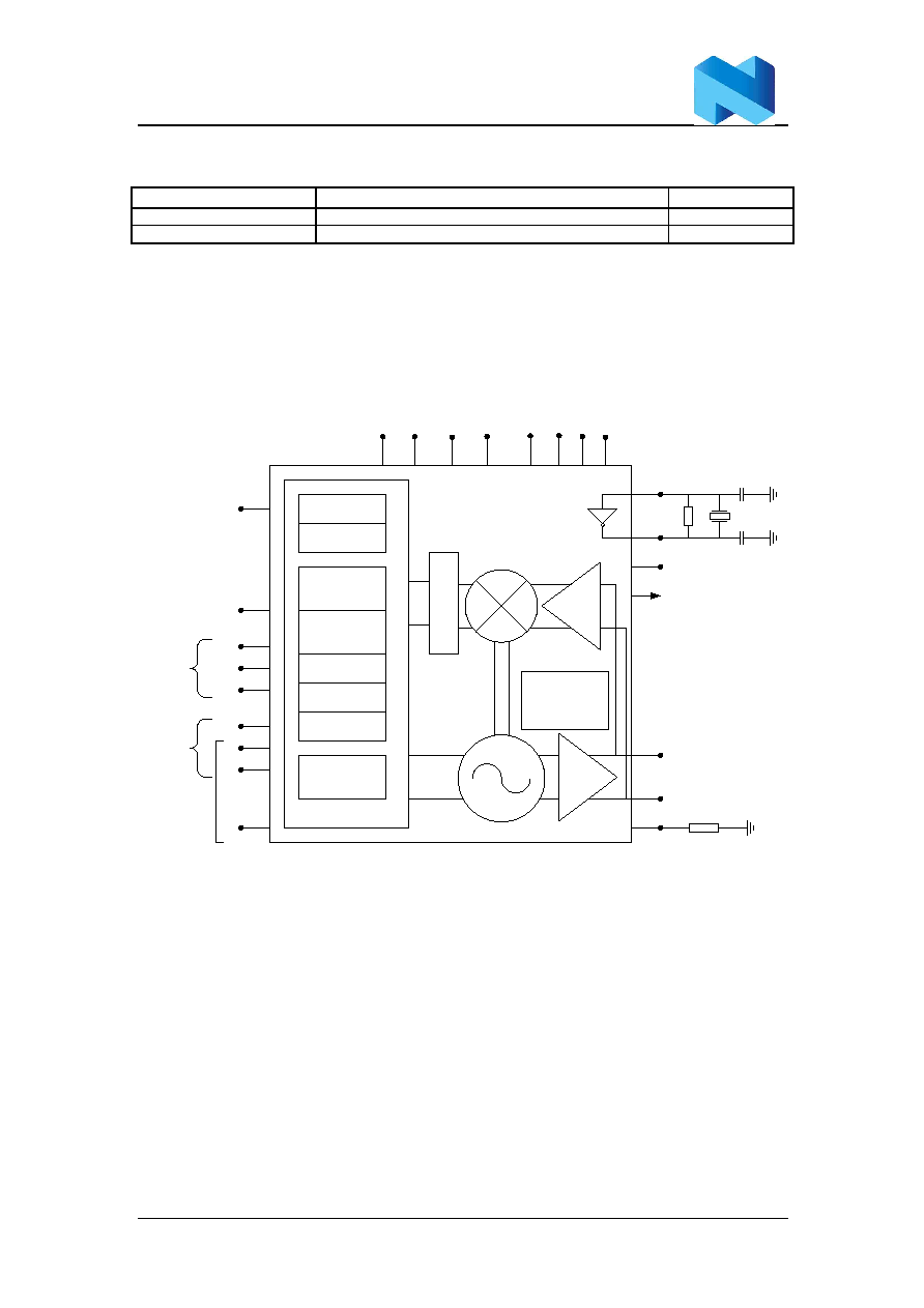
BLOCK DIAGRAM
DV
D
D
VD
D
=
3V
VD
D
=
3V
XC1
XC2
400
IREF
VDD_PA=1.8V
VSS_PA=0V
ANT1
ANT2
22k
VSS=
0V
VSS
=
0
V
VD
D
=
3V
VSS
=
0
V
VSS
=
0
V
Frequency
Synthesiser
PA
LNA
IF
B
P
F
DEMOD
Clock
Recovery,
DataSlicer
ADDR
Decode
FIFO
In/Out
CRC
Code/Decode
DuoCeiver
TM
ShockBurst
TM
GFSK
Filter
DATA
CS
CLK1
3-wire
interface
PWR_UP
CE
CLK2
DOUT2
DR2
DR1
Data
Channel 2
Data
Channel 1
Figure 1 nRF2401A with external components.

PRODUCT SPECIFICATION
nRF2401A Single Chip 2.4 GHz Radio Transceiver
Nordic Semiconductor ASA - Vestre Rosten 81, N-7075 Tiller, Norway -
Phone +4772898900
-
Fax +4772898989
Revision: 1.1
Page 3 of 40
March 2006
PIN FUNCTIONS
Pin Name
Pin function
Description
1
CE
Digital Input
Chip Enable Activates RX or TX mode
2
DR2
Digital Output
RX Data Ready at Data Channel 2 (ShockBurstTM only)
3
CLK2
Digital I/O
Clock Output/Input for RX Data Channel 2
4
DOUT2
Digital Output
RX Data Channel 2
5
CS
Digital Input
Chip Select Activates Configuration Mode
6
DR1
Digital Output
RX Data Ready at Data Channel 1 (ShockBurstTM only)
7
CLK1
Digital I/O
Clock Input (TX) & Output/Input (RX) for Data Channel 1
3-wire interface
8
DATA
Digital I/O
RX Data Channel 1/TX Data Input/ 3-wire interface
9
DVDD
Power Output
Positive Digital Supply output for de-coupling purposes
10 VSS
Power
Ground
(0V)
11
XC2
Analog Output
Crystal Pin 2
12
XC1
Analog Input
Crystal Pin 1
13
VDD_PA
Power Output
Power Supply (+1.8V) to Power Amplifier
14
ANT1
RF
Antenna interface 1
15
ANT2
RF
Antenna interface 2
16 VSS_PA Power
Ground
(0V)
17
VDD
Power
Power Supply (+3V DC)
18 VSS
Power
Ground
(0V)
19
IREF
Analog Input
Reference current
20 VSS
Power
Ground
(0V)
21
VDD
Power
Power Supply (+3V DC)
22 VSS
Power
Ground
(0V)
23
PWR_UP
Digital Input
Power Up
24
VDD
Power
Power Supply (+3V DC)
Table 3 nRF2401A pin function
PIN ASSIGNMENT
VDD
DATA
nRF2401A
QFN24 5x5
DVDD
VDD
PWR_UP
VSS
ANT2
VSS
VSS_PA
CLK1
CE
23
22
21
24
9
8
7
4
3
2
1
18
17
16
6
5
VDD_PA
ANT1
14
IREF
VSS
20
19
11
12
13
15
10
CS
XC2
XC1
DR1
DR2
CLK2
VDD
VSS
Figure 2 nRF2401A pin assignment (top view) for a QFN24 5x5 package.
PRODUCT SPECIFICATION
nRF2401A Single Chip 2.4 GHz Radio Transceiver
Nordic Semiconductor ASA - Vestre Rosten 81, N-7075 Tiller, Norway -
Phone +4772898900
-
Fax +4772898989
Revision: 1.1
Page 4 of 40
March 2006
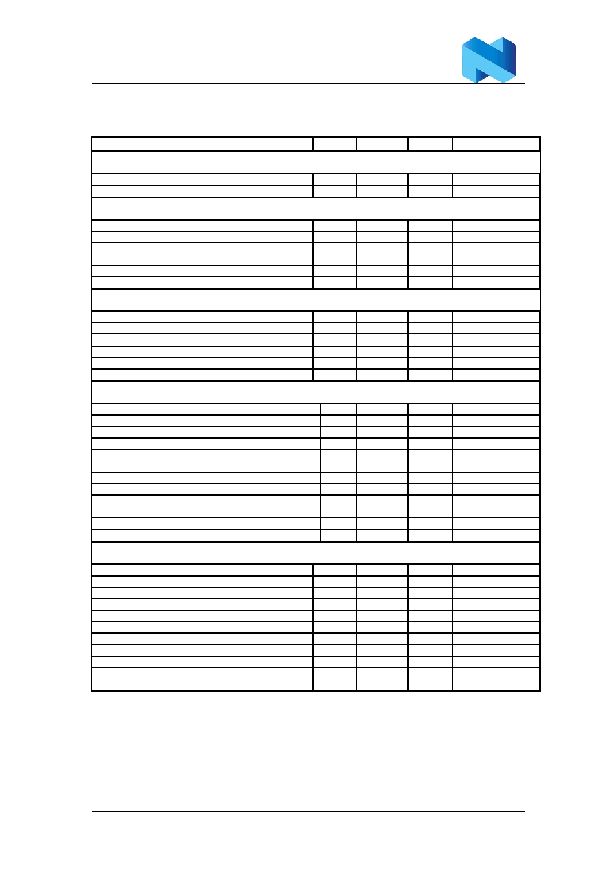
ELECTRICAL SPECIFICATIONS
Conditions: VDD = +3V, VSS = 0V, T
A
= - 40∫C to + 85∫C
Symbol Parameter
(condition)
Notes
Min.
Typ.
Max. Units
Operating conditions
VDD
Supply voltage
1.9
3.0
3.6
V
TEMP
Operating Temperature
-40
+27
+85
∫C
Digital input pin
V
IH
HIGH level input voltage
VDD- 0.3
VDD
V
V
IL
LOW level input voltage
Vss
0.3
V
Digital output pin
V
OH
HIGH level output voltage (I
OH
=-0.5mA)
VDD-
0.3
VDD
V
V
OL
LOW level output voltage (I
OL
=0.5mA) Vss
0.3
V
General RF conditions
f
OP
Operating
frequency
1)
2400
2524 MHz
f
XTAL
Crystal frequency
2)
4
20
MHz
f
Frequency deviation
±156
kHz
R
GFSK
Data rate ShockBurstTM
>0
1000
kbps
R
GFSK
Data rate Direct Mode
3)
250
1000
kbps
F
CHANNEL
Channel
spacing
1
MHz
Transmitter operation
P
RF
Maximum
Output
Power
4)
0
+4
dBm
P
RFC
RF Power Control Range
16
20
dB
P
RFCR
RF Power Control Range Resolution
±3
dB
P
BW
20dB Bandwidth for Modulated Carrier
1000
kHz
P
RF2
2
nd
Adjacent Channel Transmit Power 2MHz
-20
dBm
P
RF3
3
rd
Adjacent Channel Transmit Power 3MHz
-40
dBm
I
VDD
Supply current @ 0dBm output power
5)
13
mA
I
VDD
Supply current @ -20dBm output power
5)
8.8
mA
I
VDD
Average Supply current @ -5dBm output
power, ShockBurstTM
6) 0.8 mA
I
VDD
Average Supply current in stand-by mode
7)
12
µA
I
VDD
Average Supply current in power down
900
nA
Receiver operation
I
VDD
Supply current one channel 250kbps
18
mA
I
VDD
Supply current one channel 1000kbps
19
mA
I
VDD
Supply current two channels 250kbps
23
mA
I
VDD
Supply current two channels 1000kbps
25
mA
RX
SENS
Sensitivity at 0.1%BER (@250kbps)
-93
dBm
RX
SENS
Sensitivity at 0.1%BER (@1000kbps)
-85
dBm
C/I
CO
C/I
Co-channel
8)
10/4
dB
C/I
1ST
1
st
Adjacent Channel Selectivity C/I 1MHz
8)
-20/0
dB
C/I
2ND
2
nd
Adjacent Channel Selectivity C/I 2MHz
8)
-37/-20
dB
C/I
3RD
3
rd
Adjacent Channel Selectivity C/I 3MHz
8)
-43/-30
dB
RX
B
Blocking Data Channel 2
-45/-41
dB
1)
Usable band is determined by local regulations
2)
The crystal frequency may be chosen from 5 different values (4, 8, 12, 16, and 20MHz) which are specified in the
configuration word, see Table 8. 16MHz are required for 1Mbps operation.
3)
Data rate must be either 250kbps or 1000kbps.
4)
Antenna load impedance = 100
+j175
5)
Antenna load impedance = 100
+j175. Effective data rate 250kbps or 1Mbps.
6)
Antenna load impedance = 100
+j175. Effective data rate 10kbps.
7)
Current if 4 MHz crystal is used.
8)
250kbps/1000kbps.
Table 4 nRF2401A RF specifications
PRODUCT SPECIFICATION
nRF2401A Single Chip 2.4 GHz Radio Transceiver
Nordic Semiconductor ASA - Vestre Rosten 81, N-7075 Tiller, Norway -
Phone +4772898900
-
Fax +4772898989
Revision: 1.1
Page 5 of 40
March 2006
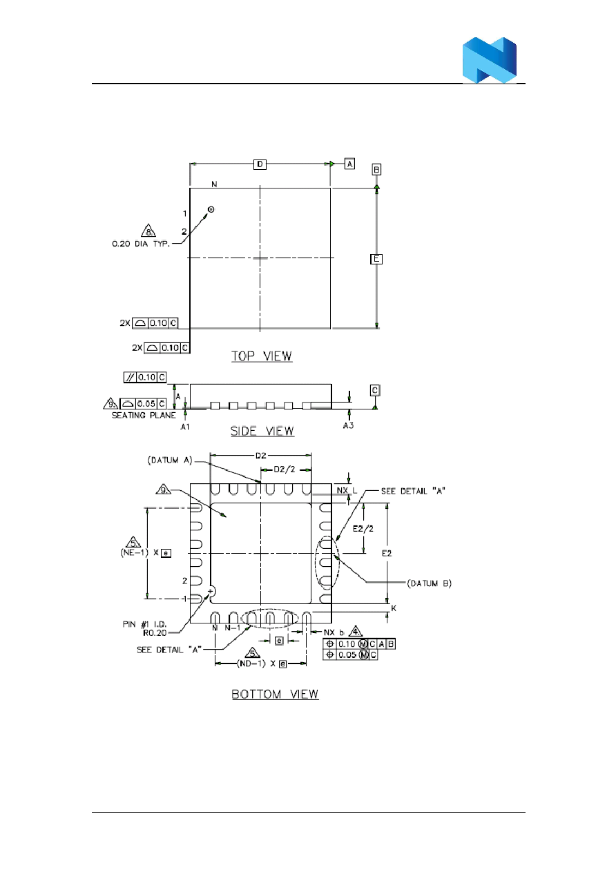
PACKAGE OUTLINE
nRF2401AG uses the QFN24 5x5 package, with matt tin plating.