 | –≠–ª–µ–∫—Ç—Ä–æ–Ω–Ω—ã–π –∫–æ–º–ø–æ–Ω–µ–Ω—Ç: nRF2402 | –°–∫–∞—á–∞—Ç—å:  PDF PDF  ZIP ZIP |
PRODUCT SPECIFICATION
Nordic VLSI ASA - Vestre Rosten 81, N-7075 Tiller, Norway - Phone +4772898900 - Fax +4772898989
Revision: 1.0
Page 1 of 25
August 2003
Single chip 2.4 GHz Transmitter
)($785(6
$33/,&$7,216
∑
True single chip GFSK transmitter in a
small 16-pin package (QFN16 4x4)
∑
Wireless mouse, keyboard, joystick
∑
Keyless entry
∑
Adjustable output power up to 0dBm
∑
Wireless data communication
∑
Data rate 0 to 1Mbps
∑
Alarm and security systems
∑
Low Bill of Material
∑
Home Automation
∑
Multi Channel operation
∑
128 channels
∑
Support frequency hopping
∑
Channel switching time <200
µ
s.
∑
Remote control
∑
Surveillance
∑
Automotive
∑
Telemetry
∑
Power supply range: 1.9 to 3.6 V
∑
CRC computation
∑
Intelligent sports equipment
∑
Industrial sensors
∑
ShockBurstTM mode for ultra-low power
operation
∑
Toy
∑
Low supply current, typical 10mA peak
@ -5dBm output power
∑
World wide use
*(1(5$/ '(6&5,37,21
nRF2402 is a single-chip radio transmitter for the world wide 2.4 - 2.5 GHz ISM
band. The transmitter consists of a fully integrated frequency synthesizer, a power
amplifier, a crystal oscillator and a modulator. Output power and frequency channel is
easily programmable by use of the 3-wire interface. Current consumption is very low,
only 10 mA at an output power of -5dBm. Built-in ShockBurstTM and Power Down
modes makes power saving easily realizable.
48,&. 5()(5(1&( '$7$
3DUDPHWHU
9DOXH
8QLW
Minimum supply voltage
1.9
V
Maximum output power
0
dBm
Maximum GFSK data rate
1000
kbps
Supply current GFSK transmitter @ -5dBm output power
10
mA
Supply current in Power Down mode
200
n
Table 1 nRF2402 quick reference data
7\SH 1XPEHU
'HVFULSWLRQ
9HUVLRQ
nRF2402 IC
16 pin QFN 4x4
A
Table 2 nRF2402 ordering information
Q5)
PRODUCT SPECIFICATION
Q5) 6LQJOH &KLS *+] 5DGLR 7UDQVPLWWHU
Nordic VLSI ASA - Vestre Rosten 81, N-7075 Tiller, Norway - Phone +4772898900 - Fax +4772898989
Revision: 1.0
Page 2 of 25
August 2003
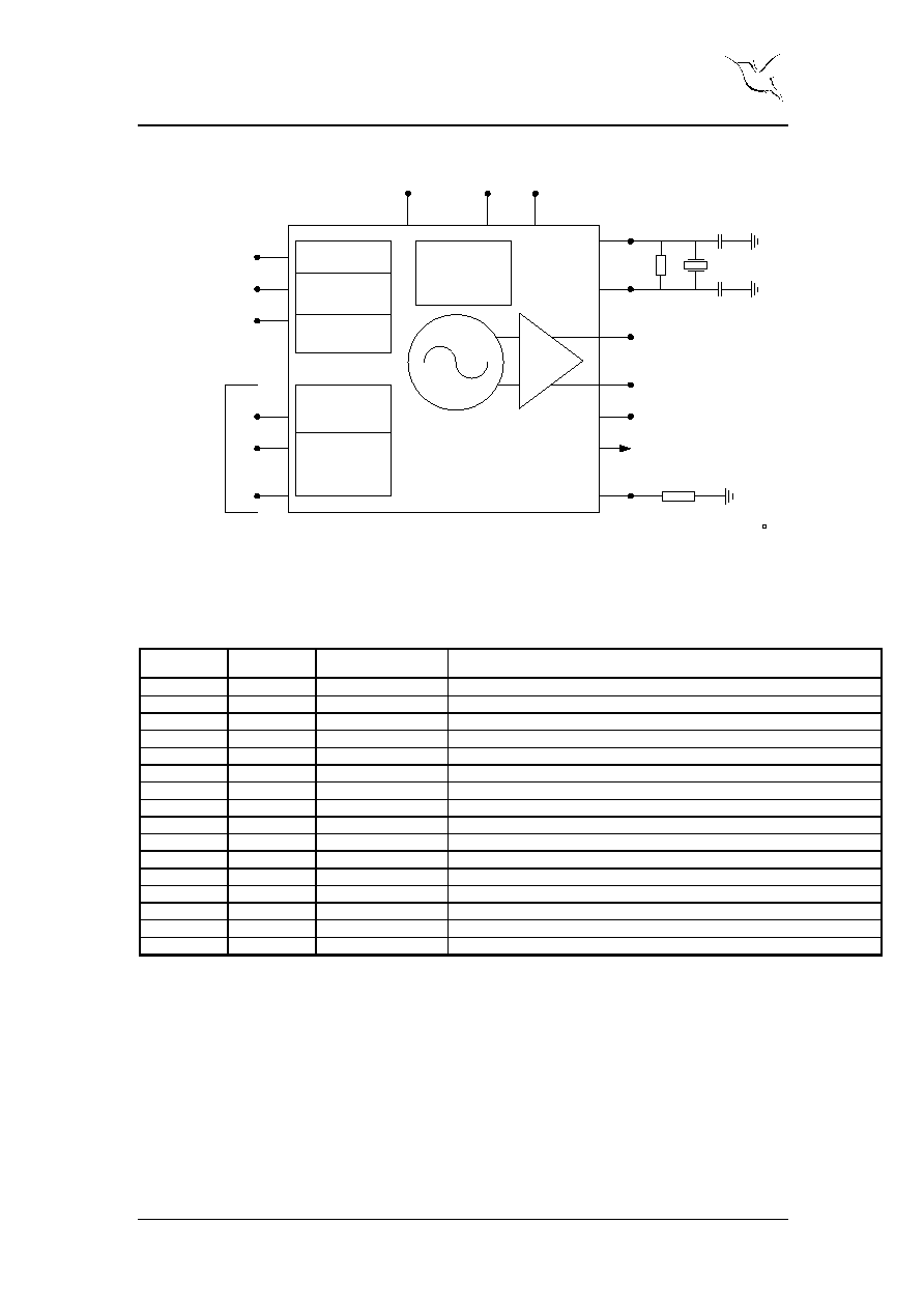
%/2&. ',$*5$0
400
VDD=3V
XC1
VSS=0V
IREF
VDD_PA=1.8V
VSS_PA=0V
PA
Frequency
Synthesiser
VDD=3V
XC2
ANT1
ANT2
22k
FIFO
In
CRC
Code
ShockBurst
TM
DIN
CLK
CS
3-wire
Interface
PWR_UP
CE
VSS=0V
3-wire
Programming
Interface
GFSK
Filter
Figure 1 nRF2402 with external components.
3,1 )81&7,216
3LQ
1DPH
3LQ IXQFWLRQ
'HVFULSWLRQ
1
CE
Input
Chip Enable Activates TX mode
2
CS
Input
Chip Select Activates Configuration Mode
3
CLK
Input
Clock Input TX Data and 3-wire Interface
4
DIN
Input
TX Data Input / Configuration Data Input
5
VSS
Power
Ground (0V)
6
XC2
Output
Crystal pin 2
7
XC1
Input
Crystal pin 1
8
VDD
Power
Power Supply (+3V DC)
9
VSS_PA
Power
Ground (0V)
10
ANT1
Power/RF
Antenna output 1
11
ANT2
Power/RF
Antenna output 2
12
VDD_PA
Power Output
Power Supply (+1.8V DC) to the PA
13
VDD
Power
Power Supply (+3V DC)
14
IREF
Input
Reference current
15
VSS
Power
Ground (0V)
16
PWR_UP
Input
Power Up
Table 3 nRF2402 pin functions
PRODUCT SPECIFICATION
Q5) 6LQJOH &KLS *+] 5DGLR 7UDQVPLWWHU
Nordic VLSI ASA - Vestre Rosten 81, N-7075 Tiller, Norway - Phone +4772898900 - Fax +4772898989
Revision: 1.0
Page 3 of 25
August 2003
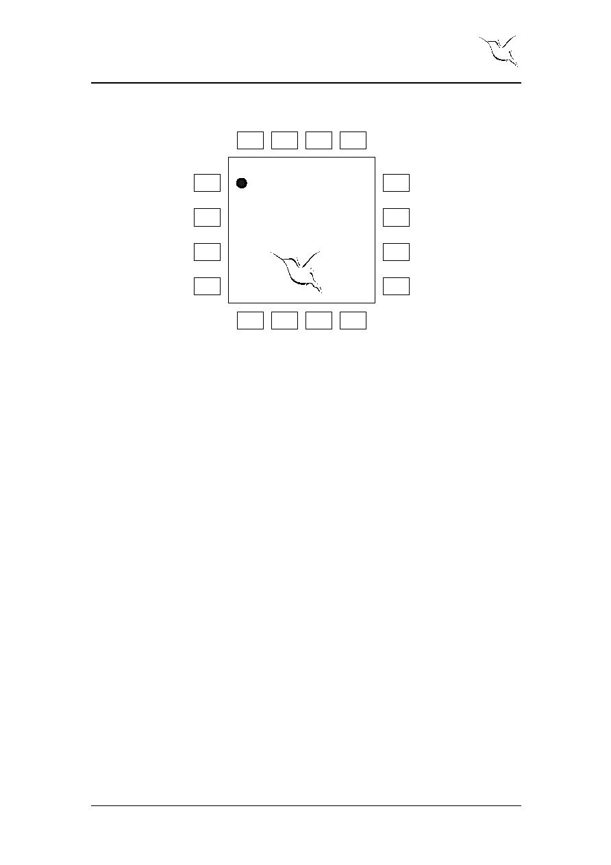
3,1
$66,*10(17
CE
CLK
CS
VSS
VDD
DIN
XC1
Q5)
QFN16 4x4
VDD
ANT2
PWR_UP
VDD_PA
VSS_PA
XC2
ANT1
VSS
IREF
15
14
13
16
8
7
6
5
4
3
2
1
12
11
10
9
Figure 2. nRF2402 pin assignment (top view).

PRODUCT SPECIFICATION
Q5) 6LQJOH &KLS *+] 5DGLR 7UDQVPLWWHU
Nordic VLSI ASA - Vestre Rosten 81, N-7075 Tiller, Norway - Phone +4772898900 - Fax +4772898989
Revision: 1.0
Page 4 of 25
August 2003
(/(&75,&$/ 63(&,),&$7,216
Conditions: VDD = +3V, VSS = 0V, T
A
= - 40∫C to + 85∫C
6\PERO 3DUDPHWHU FRQGLWLRQ�
1RWHV
0LQ
7\S
0D[
8QLWV
2SHUDWLQJ FRQGLWLRQV
VDD
Supply voltage
1.9
3.0
3.6
V
TEMP
Operating Temperature
-40
+27
+85
∫C
'LJLWDO LQSXW SLQ
V
IH
HIGH level input voltage
VDD- 0.3
VDD
V
V
IL
LOW level input voltage
Vss
0.3
V
'LJLWDO RXWSXW SLQ
V
OH
HIGH level output voltage (I
OH
=-0.5mA)
VDD- 0.3
VDD
V
V
OL
LOW level output voltage (I
OL
=0.5mA)
Vss
0.3
V
*HQHUDO 5) FRQGLWLRQV
f
OP
Operating frequency
1)
2400
2527
MHz
f
XTAL
Crystal frequency
2)
4
20
MHz
f
Frequency deviation
±115
±156
±175
kHz
R
GFSK
GFSK data rate ShockBurstTM
>0
1000
kbps
R
GFSK
GFSK data rate Direct Mode
3)
250
1000
kbps
F
CHANNEL
Channel spacing
1
MHz
7UDQVPLWWHU RSHUDWLRQ
P
RF
Maximum Output Power
4)
0
+4
dBm
P
RFC
RF Power Control Range
16
20
dB
P
RFCR
RF Power Range Control Resolution
±3
dB
P
BW
20dB Bandwidth for Modulated Carrier
1000
kHz
P
RF2
2
nd
Adjacent Channel Transmit Power 2MHz
-20
dBc
P
RF3
3
rd
Adjacent Channel Transmit Power 3MHz
-40
dBc
I
VDD
Supply current @ 0dBm output power
5)
11.5
13
mA
I
VDD
Supply current @ -5dBm output power
5)
10.0
11
mA
I
VDD
Average Supply current @ -5dBm output
power, ShockBurstTM
6)
500
µ
A
I
VDD
Average Supply current in stand-by mode
12
µ
A
I
VDD
Average Supply current in power down
200
nA
NOTES:
1)
Usable band is determined by local regulations
2)
The crystal frequency may be chosen from 5 different values (4, 8, 12, 16, and 20MHz) which are specified in
the configuration word, see Table 8. 16MHz are required
for 1Mbps operation.
3)
Data rate must be either 250kbps or 1000kbps.
4)
Antenna load impedance = 400
5)
Antenna load impedance = 400
. Effective data rate 250kbps or 1Mbps.
6)
Antenna load impedance = 400
. Effective data rate 10kbps.
Table 4 nRF2402 electrical specifications
PRODUCT SPECIFICATION
Q5) 6LQJOH &KLS *+] 5DGLR 7UDQVPLWWHU
Nordic VLSI ASA - Vestre Rosten 81, N-7075 Tiller, Norway - Phone +4772898900 - Fax +4772898989
Revision: 1.0
Page 5 of 25
August 2003
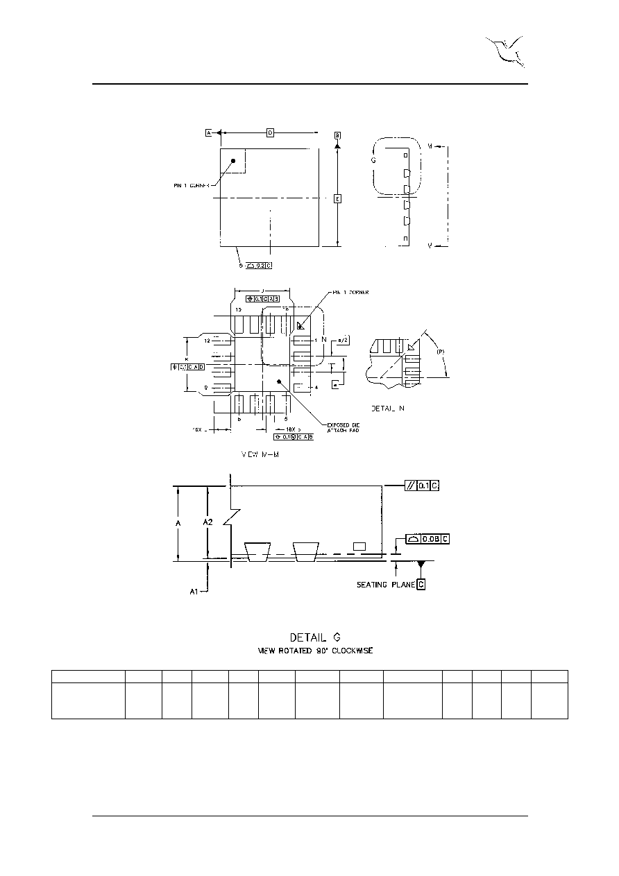
3$&.$*( 287/,1(
nRF2402, uses the QFN16 4x4 package. Dimensions are in mm.
3DFNDJH 7\SH
$
$
$
E
'
(
H
-
.
/
3
QFN16
(4x4 mm)
0LQ
W\S
0D[
0.8
1
0.0
0.05
0.75
1
0.23
0.3
0.38
4 BSC
4 BSC
0.65 BSC
0.75
2.25
0.7
2.25
0.45
0.55
0.75
45
∞
REF
Figure 3 nRF2402 Package outline.