
PRELIMINARY PRODUCT SPECIFICATION
Nordic Semiconductor ASA - Vestre Rosten 81, N-7075 Tiller, Norway -
Phone +4772898900
-
Fax +4772898989
Revision: 2.0
Page 1 of 37
April 2005
Single chip 2.4 GHz Transceiver
with Embedded ANT protocol
FEATURES
∑ Integrated PAN (Personal Area
Network)
∑ Drop in wireless networking with
simple serial interface
∑ 2.4GHz Worldwide ISM Band
∑ Ultra-low power (coin cell battery)
∑ Fully scaleable
∑ Broadcast, Acknowledged or Burst
Data
∑ Message rates 0.5Hz -> 200Hz
(8byte data payload)
∑ Burst transfer rates up to 20kbps
(true data throughput)
∑ Public and private networks
∑ 1 Mbps RF data rate
∑ 125 RF channels
APPLICATIONS
∑ Sensor Networks
∑ Industrial Automation
∑ Home Automation
∑ Sports Monitoring
GENERAL DESCRIPTION
The nRF24AP1 is an ultra-low power single-chip radio transceiver with embedded ANT
protocol for personal area networks. The transceiver's RF operating frequency range falls
within the world-wide 2.4 - 2.5 GHz RF ISM band, allowing for regulatory compliance
and product sales into global markets.
QUICK REFERENCE DATA
Parameter Value
Unit
Minimum supply voltage
1.9
V
Maximum output power
0
dBm
Maximum data rate (over the air)
1000
kbps
Temperature range
-40 to +85
∞C
Sensitivity -80
dBm
Average current consumption as low as
40
µA
Peak current consumption TX @-5dBm
13.5mA for 350us
mA
Peak current consumption RX
22mA for 600us
mA
Max # of simultaneous connections
1
>65000
connections
Max # of simultaneous independent 2-way connections
4
2-way connections
Maximum sustained transfer rate (all data ≠ no overhead)
2
20
kbps
CR2032 Battery life in a typical sensor application
3
5 years
Table 1: nRF24AP1 quick reference data
1
Using Shared Channel Network
2
Transfer rate refers to data rate of the end application's message payload
3
Message interval of 2s, 1 hour/day usage
Simple Networks
Complex
Networks
Independent Networks
Broadcast
Networks
Shared Channel
Networks
nRF24AP1
ANT by Dynastream
© 2005 all rights reserved
PRELIMINARY PRODUCT SPECIFICATION
nRF24AP1 Single Chip 2.4 GHz Radio Transceiver with Embedded ANT Protocol
Nordic Semiconductor ASA - Vestre Rosten 81, N-7075 Tiller, Norway -
Phone +4772898900
-
Fax +4772898989
Revision: 2.0
Page 2 of 37
April 2005
The transceiver consists of the ANT fully integrated protocol engine, frequency
synthesizer, power amplifier, crystal oscillator and modulator, and can be interfaced to a
host microcontroller over either a synchronous or asynchronous serial interface. Designed
to run on a wrist-watch coin cell battery, current consumption of the device is extremely
low - a typical sensor application can operate on approximately 40µA average current
consumption. Short, low peak current transitions are battery friendly.
The embedded ANT protocol makes for easy, low cost integration. Eliminating the need
for 3
rd
party RF protocol implementation, the on-chip ANT protocol combined with the
2.4GHz transceiver enables system and application developers to interact with the
nRF24AP1 as a black box wireless solution. The simple serial interface (asynchronous or
synchronous) to the device allows for flexibility and scalability from ultra-low power
sensors (40µA) through to higher data rate (20kbps) applications implemented in a
multitude of network configurations. Networks can be scaled from as little as two nodes
to thousands. With 2
32
unique IDs, multiple radio frequencies, public and private network
management and scalable data rates, an unlimited number of network configurations and
applications are possible.
Prior to reading this document, the "ANT Message Protocol and Usage" document should
be read to gain understanding of the ANT protocol capabilities.
ORDERING INFORMATION
Type Number
Description
Version
nRF24AP1
24 pin QFN 5x5, lead free (green)
A
nRF24AP1-EVKIT
4 node network evaluation and development kit
A
Table 2: nRF24AP1 ordering information

PRELIMINARY PRODUCT SPECIFICATION
nRF24AP1 Single Chip 2.4 GHz Radio Transceiver with Embedded ANT Protocol
Nordic Semiconductor ASA - Vestre Rosten 81, N-7075 Tiller, Norway -
Phone +4772898900
-
Fax +4772898989
Revision: 2.0
Page 3 of 37
April 2005
TABLE OF CONTENTS
1.
BLOCK DIAGRAM ...............................................................................................................................4
2. PIN FUNCTIONS ...................................................................................................................................5
3.
PIN ASSIGNMENT................................................................................................................................5
4.
ELECTRICAL SPECIFICATIONS ........................................................................................................6
5.
PACKAGE OUTLINE............................................................................................................................7
6.
ABSOLUTE MAXIMUM RATINGS ....................................................................................................8
7.
ARCHITECTURAL OVERVIEW........................................................................................................10
8.
ANT INTERFACE................................................................................................................................11
8.1
Physical Layer ≠ Serial Interfacing ................................................................................................. 11
8.2
ANT Message Summary ................................................................................................................. 11
8.3
Message Summary .......................................................................................................................... 12
9.
APPLICATION SPECIFIC CURRENT CONSUMPTION..................................................................13
10.
ASYNCHRONOUS SERIAL COMMUNICATION .....................................................................14
10.1
Description ................................................................................................................................. 14
10.2
Interconnect ................................................................................................................................ 14
10.3
Port Select (PORTSEL).............................................................................................................. 14
10.4
Speed Select (BR1,BR2) ............................................................................................................ 14
10.5
Suspend Control (
SUSPEND
)................................................................................................. 15
10.6
32kHz Clock Signal (EXT32K) ................................................................................................. 15
10.7
Asynchronous Port Control (RTS) ............................................................................................. 15
10.8
SLEEP ENABLE (SLEEP) ........................................................................................................ 16
10.9
Link Layer Protocol ................................................................................................................... 17
10.10
ANT Messages ........................................................................................................................... 18
11.
SYNCHRONOUS SERIAL COMMUNICATION ........................................................................19
11.1
Description ................................................................................................................................. 19
11.2
Interconnect ................................................................................................................................ 19
11.3
Port Select (PORTSEL).............................................................................................................. 19
11.4
Flow Control Select (SFLOW)................................................................................................... 20
11.5
32kHz Clock Signal (EXT32K) ................................................................................................. 20
11.6
Operating Mechanism ................................................................................................................ 20
11.7
Power Down / Power Up............................................................................................................ 20
11.8
General Synchronous Port Operation ......................................................................................... 21
11.9
Link Layer Protocol ................................................................................................................... 21
11.10
ANT Messages ........................................................................................................................... 23
11.11
Synchronous Messaging with Byte Flow Control ..................................................................... 23
11.12
Synchronous Messaging with Bit Flow Control........................................................................ 26
11.13
Optional Serial Enable Control (ANT
HOST) ...................................................................... 26
11.14
Synchronization.......................................................................................................................... 27
11.15
Using an Epson MCU as a host controller ................................................................................. 27
12.
PERIPHERAL RF INFORMATION..............................................................................................29
12.1
Antenna output ........................................................................................................................... 29
12.2
Output Power adjustment ........................................................................................................... 29
12.3
Crystal Specification .................................................................................................................. 29
12.4
Sharing crystal with micro controller. ........................................................................................ 30
12.5
Crystal parameters:..................................................................................................................... 30
12.6
Input crystal amplitude & Current consumption ........................................................................ 30
12.7
PCB layout and de-coupling guidelines ..................................................................................... 31
13.
APPLICATION EXAMPLE...........................................................................................................32
13.1
nRF24AP1 with single ended matching network ....................................................................... 32
13.2
PCB layout example................................................................................................................... 34
14.
DEFINITIONS................................................................................................................................35
14.1
Nordic Semiconductor ASA ≠ World Wide Distributors ........................................................... 37
PRELIMINARY PRODUCT SPECIFICATION
nRF24AP1 Single Chip 2.4 GHz Radio Transceiver with Embedded ANT Protocol
Nordic Semiconductor ASA - Vestre Rosten 81, N-7075 Tiller, Norway -
Phone +4772898900
-
Fax +4772898989
Revision: 2.0
Page 5 of 37
April 2005
2.
PIN FUNCTIONS
Pin Name
Pin function
Description
1
BR2 / SCLK
Digital IO
Asynchronous baud rate select / Synchronous clock signal
2
BR1 / SFLOW
Digital Input
Asynchronous baud rate select / Synch. Bit or byte flow select
3
EXT32K
Digital Input
Optional External 32kHz clock, tied to GND when not used
4
RXD / SIN
Digital Input
Asynchronous UART receive data / Synchronous receive data
5
TXD / SOUT
Digital Output
Asynchronous UART transmit data / Synchronous transmit data
6
SUSPEND / SRDY
Digital Input
Asynchronous suspend control / Synchronous port ready signal
7
SLEEP / SMSGRDY
Digital Input
Asynchronous sleep enable / Synchronous message ready signal
8
RTS / SEN
Digital Output
Asynchronous flow control RTS /Synchronous serial enable
9
DVDD
Power Output
Positive Digital Supply output for de-coupling purposes
10 VSS
Power
Ground
(0V)
11
XC2
Analog Output
Crystal Pin 2
12
XC1
Analog Input
Crystal Pin 1
13
VDD_PA
Power Output
Power Supply (+1.8V) to Power Amplifier
14
ANT1
RF
Antenna interface 1
15
ANT2
RF
Antenna interface 2
16 VSS_PA
Power
Ground
(0V)
17
VDD
Power
Power Supply (+3V DC)
18 VSS
Power
Ground
(0V)
19
IREF
Analog Input
Reference current
20 VSS
Power
Ground
(0V)
21
VDD
Power
Power Supply (+3V DC)
22 VSS
Power
Ground
(0V)
23
PORTSEL
Digital Input
Asynchronous / Synchronous port selection
24
VDD
Power
Power Supply (+3V DC)
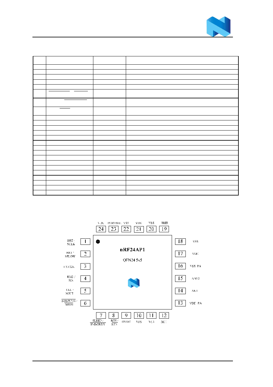
Table 3: nRF24AP1 pin function
3.
PIN ASSIGNMENT
Figure 2: nRF24AP1 pin assignment (top view) for a QFN24 5x5 package.
