
OKI Semiconductor
FEDSMS81V26000-02
Issue Date: Dec 15, 2004
MS81V26000
1,114,112-Word
◊
24-Bit Field Memory
1/20
GENERAL DESCRIPTION
The OKI MS81V26000 is a high performance 26-Mbit, 1,100K
◊
24-bit, Field Memory. It is especially designed
for high-speed serial access applications such as HDTVs, conventional NTSC TVs, VTRs, digital movies and
Multi-media systems. MS81V26000 is a FRAM for wide or low end use in general commodity TVs and VTRs
exclusively. MS81V26000 is not designed for the other use or high end use in medical systems, professional
graphics systems which require long term picture storage, data storage systems and others. More than two
MS81V26000s can be cascaded directly without any delay devices among the MS81V26000s. (Cascading of
MS81V26000 provides larger storage depth or a longer delay).
Each of the 24-bit planes has separate serial write and read ports. These employ independent control clocks to
support asynchronous read and write operations. Different clock rates are also supported that allow alternate data
rates between write and read data streams.
The MS81V26000 provides high speed FIFO, First-In First-Out, operation without external refreshing:
MS81V26000 refreshes its DRAM storage cells automatically, so that it appears fully static to the users.
Moreover, fully static type memory cells and decoders for serial access enable the refresh free serial access
operation, so that serial read and/or write control clock can be halted high or low for any duration as long as the
power is on. Internal conflicts of memory access and refreshing operations are prevented by special arbitration
logic.
The MS81V26000's function is simple, and similar to a digital delay device whose delay-bit-length is easily set by
reset timing. The delay length, number of read delay clocks between write and read, is determined by externally
controlled write and read reset timings.
Additionally, the MS81V26000 has write mask function or input enable function (IE), and read-data skipping
function or output enable function (OE) . The differences between write enable (WE) and input enable (IE), and
between read enable (RE) and output enable (OE) are that WE and RE can stop serial write/read address
increments, but IE and OE cannot stop the increment, when write/read clocking is continuously applied to
MS81V26000. The input enable (IE) function allows the user to write into selected locations of the memory only,
leaving the rest of the memory contents unchanged. This facilitates data processing to display a "picture in picture"
on a TV screen.

FEDS81V26000-02
OKI Semiconductor
MS81V26000
2/20
FEATURES
∑
Single power supply: 3.3 V
±
0.3 V
∑
1,114,112
words
◊
24 bits
∑
Fast FIFO (First-In First-Out) operation
∑
High speed asynchronous serial access
Read/write cycle time 12 ns
Access
time
9
ns
∑
Randomly accessible leading address
∑
Variable length delay bit (350 to 1,114,112)
∑
Write/Read start address settable
∑
Write mask function (Input enable control)
∑
Data skipping function (Output enable control)
∑
Self refresh (No refresh control is required)
∑
Package
options:
100-pin plastic TQFP
(TQFP100-P-1414-0.50-K) (MS81V26000-xxTB)
xx indicates speed rank.
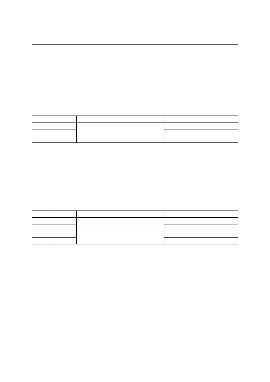
PRODUCT FAMILY
Family
Access Time (Max.)
Cycle Time (Min.)
Package
MS81V26000-12TB
9 ns
12 ns (83 MHz)
100-pin TQFP

FEDS81V26000-02
OKI Semiconductor
MS81V26000
3/20
PIN CONFIGURATION (TOP VIEW)
Pin Name
Function
SWCK
Serial Write Clock
SRCK
Serial Read Clock
WE Write
Enable
RE Read
Enable
IE Input
Enable
OE Output
Enable
RSTW
Write Reset Clock
RSTR
Read Reset Clock
WAD
Write Address Input
RAD
Read Address Input
D
IN
0 to 23
Data Input
D
OUT
0 to 23
Data Output
V
CC
Power Supply (3.3 V)
V
SS
Ground (0 V)
V
CC
Q
Power Supply for output
V
SS
Q
Ground for output
NC No
Connection
Note: The same power supply voltage must be provided to every V
CC
pin and V
CC
Q pin, and the same
GND voltage level must be provided to every V
SS
pin and V
SS
Q pin.
V
SS
DI4
DI5
DI6
DI7
V
SS
DI8
DI9
DI10
DI1
1
V
SS
V
CC
NC
NC
V
SS
V
CC
V
SS
Q
DO1
1
DO10
V
CC
Q
DO9
DO8
V
SS
Q
DO7
DO6
100-Pin TQFP
1
2
3
4
5
6
7
8
9
10
11
12
13
14
15
16
17
18
19
20
21
22
23
24
25
75
74
73
72
71
70
69
68
67
66
65
64
63
62
61
60
59
58
57
56
55
54
53
52
51
V
CC
DI3
DI2
DI1
DI0
V
SS
WAD
IE
WE
RSTW
V
CC
SWCK
V
SS
SRCK
V
CC
RSTR
RE
OE
RAD
V
SS
DI12
DI13
DI14
DI15
V
CC
100
99
98
97
96
95
94
93
92
91
90
89
88
87
86
85
84
83
82
81
80
79
78
77
76
26
27
28
29
30
31
32
33
34
35
36
37
38
39
40
41
42
43
44
45
46
47
48
49
50
V
SS
DI16
DI17
DI18
DI19
V
SS
DI20
DI21
DI22
DI23
V
SS
V
CC
NC
NC
V
SS
V
CC
V
SS
Q
DO23
DO22
V
CC
Q
DO21
DO20
V
SS
Q
DO19
DO18
V
CC
V
CC
Q
DO5
DO4
V
SS
Q
V
SS
DO3
DO2
V
CC
Q
DO1
DO0
V
SS
V
SS
Q
V
CC
DO12
DO13
V
CC
Q
DO14
DO15
V
SS
V
SS
Q
DO16
DO17
V
CC
Q
V
CC

FEDS81V26000-02
OKI Semiconductor
MS81V26000
4/20
BLOCK DIAGRAM
Refresh
Counter
Data-output
Buffer
Read Data Register
X
Decoder
(X24)
Serial Read Controller
(X24)
Serial Write Controller
Data-input
Buffer
Read/Write
Refresh
Timing Generater
DO (X24)
OE
RE
RSTR
SRCK
DI (X24)
IE
WE
RSTW
SWCK
1,114,112 x 24
Memory
Array
Write Data Register
RAD
WAD

FEDS81V26000-02
OKI Semiconductor
MS81V26000
5/20
PIN DESCRIPTION
Serial Write Clock: SWCK
The SWCK latches the input data on chip when WE is high, and also increments the internal write address pointer.
Data-in setup time tDS, and hold time tDH are referenced to the rising edge of SWCK.
Write Reset: RSTW
RSTW is used to set the internal write address pointer. RSTW setup and hold times are referenced to the rising
edge of SWCK. The SWCK latches the write address data (21bits serial LSB) from WAD.
Write Enable: WE
WE is used for data write enable/disable control. WE high level enables the input, and WE low level disables the
input and holds the internal write address pointer. There are no WE disable time (low) and WE enable time (high)
restrictions, because the MS81V26000 is in fully static operation as long as the power is on. Note that WE setup
and hold times are referenced to the rising edge of SWCK. The latency for the write operation control by WE is 4.
After write reset, WE must remain low for more than 1600 ns (tFWD). After write reset, the write operation at
address 0 is started after a time tWL form the cycle in which WE is brought high.
After write reset, WE should be remained high for 2 cycles after driving WE high first.
Input Enable: IE
IE is used to enable/disable writing into memory. IE high level enables writing. The internal write address pointer
is always incremented by cycling SWCK regardless of the IE level. Note that IE setup and hold times are
referenced to the rising edge of SWCK. The latency for the write operation control by IE is 4.
Write Address Input: WAD
These pins are used for write address input.
Data Inputs: (DI0-23)
These pins are used for serial data inputs.
Write Reset: RSTW
RSTW is used to set the internal write address pointer. RSTW setup and hold times are referenced to the rising
edge of SWCK. The SWCK latches the write address data (21bits serial LSB) from WAD.
Data Out: (DO0-23)
These pins are used for serial data outputs.
Serial Read Clock: SRCK
Data is shifted out of the data registers. It is triggered by the rising edge of SRCK when RE is high during a read
operation. The SRCK input increments the internal read address pointer when RE is high.
The three-state output buffer provides direct TTL compatibility (no pullup resistor required). Data out is the same
polarity as data in. The output becomes valid after the access time interval tAC that begins with the rising edge of
SRCK. *There are no output valid time restriction on MS81V26000.
Read Reset: RSTR
RSTR is used to set the internal read address pointer. RSTR setup and hold times are referenced to the rising edge
of SRCK. The SWCK latches the read address data (21bits serial LSB) from RAD.
Read Enable: RE
The function of RE is to gate of the SRCK clock for incrementing the read pointer. When RE is high before the
rising edge of SRCK, the read pointer is incremented. When RE is low, the read pointer is not incremented. RE
setup times (tRENS and tRDSS) and RE hold times (tRENH and tRDSH) are referenced to the rising edge of the
SRCK clock.

FEDS81V26000-02
OKI Semiconductor
MS81V26000
6/20
The latency for the read operation control by RE is 4. After read reset, RE must remain low for more than 1600 ns
(tFRD). After read reset, the read data at address 0 is output after a time tRL from the cycle in which WE is brought
high.
After read reset, RE should be remained high for 2 cycles after driving RE high first.
Output Enable: OE
OE is used to enable/disable the outputs. OE high level enables the outputs. The internal read address pointer is
always incremented by cycling SRCK regardless of the OE level. Note that OE setup and hold times are referenced
to the rising edge of SRCK. The latency for the read operation control by OE is 4.
Read Address Input: RAD
These pins are used for read address input.

FEDS81V26000-02
OKI Semiconductor
MS81V26000
7/20
ELECTRICAL CHARACTERISTICS
Absolute Maximum Ratings
Parameter Symbol
Conditon
Rating Unit
Power Supply Voltage
V
CC
Ta
=
25
∞
C
≠0.5 to +4.6
V
Input Output Voltage
V
T
at Ta = 25
∞
C, V
SS
≠0.5 to +4.6
V
Output Current
I
OS
Ta
=
25
∞
C 50
mA
Power Dissipation
P
D
Ta
=
25
∞
C 1
W
Operating Temperature
T
opr
--
0 to 70
∞
C
Storage Temperature
T
stg
--
≠55 to +150
∞
C
Recommended Operating Conditions
Parameter Symbol
Min.
Typ
Max. Unit
Power Supply Voltage
V
CC
3.0
3.3
3.6
V
Input High Voltage
V
IH
2.0
V
CC
V
CC
+ 0.3
V
Input Low Voltage
V
IL
≠0.3
0
+0.8 V
DC Characteristics
Parameter Symbol
Condition Min.
Max.
Unit
Input Leakage Current
I
LI
0 < V
I
< V
CC
+ 0.3 V, Other Pins Tested at V = 0 V
≠10
+10
µA
Output Leakage Current
I
LO
0 < V
O
< V
CC
≠10
+10
µA
Output "H" Level Voltage
V
OH
I
OH
= ≠2 mA
2.4
--
V
Output "L" Level Voltage
V
OL
I
OL
= 2 mA
--
0.4
V
Operating Current
I
CC1
Minimum Cycle Time, Output Open
--
200
mA
Standby Current
I
CC2
Input Pin = V
IH
/V
IL
--
5
mA
Capacitance
(V
CC
= 3.3 V
±
0.3 V, Ta = 25
∞
C, f = 1 MHz)
Parameter Symbol
Max.
Unit
Input Capacitance
C
I
6 pF
Output Capacitance
C
O
7 pF

FEDS81V26000-02
OKI Semiconductor
MS81V26000
8/20
AC Characteristics
(V
CC
= 3.3 V
±
0.3 V, Ta = 0 to 70
∞
C)
MS81V26000-12
Parameter Symbol
Min. Max.
Unit
Access Time from SRCK
t
AC
-- 9
ns
D
OUT
Hold Time from SRCK
t
DDCK
3 --
ns
D
OUT
Enable Time from SRCK
t
DECK
3 9
ns
SWCK "H" Pulse Width
t
WSWH
4 --
ns
SWCK "L" Pulse Width
t
WSWL
4 --
ns
Input Data Setup Time
t
DS
3
--
ns
Input Data Hold Time
t
DH
1
--
ns
WE Enable Setup Time
t
WENS
3 --
ns
WE Enable Hold Time
t
WENH
1 --
ns
WE Disable Setup Time
t
WDSS
3 --
ns
WE Disable Hold Time
t
WDSH
1 --
ns
IE Enable Setup Time
t
IENS
3 --
ns
IE Enable Hold Time
t
IENH
1 --
ns
IE Disable Setup Time
t
IDSS
3 --
ns
IE Disable Hold Time
t
IDSH
1 --
ns
WE "H" Pulse Width
t
WWEH
4 --
ns
WE "L" Pulse Width
t
WWEL
4 --
ns
IE "H" Pulse Width
t
WIEH
4 --
ns
IE "L" Pulse Width
t
WIEL
4 --
ns
RSTW Setup Time
t
RSTWS
3 --
ns
RSTW Hold Time
t
RSTWH
1 --
ns
SRCK "H" Pulse Width
t
WSRH
4 --
ns
SRCK "L" Pulse Width
t
WSRL
4 --
ns
RE Enable Setup Time
t
RENS
3 --
ns
RE Enable Hold Time
t
RENH
1 --
ns
RE Disable Setup Time
t
RDSS
3 --
ns
RE Disable Hold Time
t
RDSH
1 --
ns
OE Enable Setup Time
t
OENS
3 --
ns
OE Enable Hold Time
t
OENH
1 --
ns
OE Disable Setup Time
t
ODSS
3 --
ns
OE Disable Hold Time
t
ODSH
1 --
ns
RE "H" Pulse Width
t
WREH
4 --
ns
RE "L" Pulse Width
t
WREL
4 --
ns
OE "H" Pulse Width
t
WOEH
4 --
ns
OE "L" Pulse Width
t
WOEL
4 --
ns
RSTR Setup Time
t
RSTRS
3 --
ns
RSTR Hold Time
t
RSTRH
1 --
ns
SWCK Cycle Time
t
SWC
12 --
ns
SRCK Cycle Time
t
SRC
12 --
ns
Transition Time (Rise and Fall)
t
T
1
5
ns

FEDS81V26000-02
OKI Semiconductor
MS81V26000
9/20
MS81V26000-12
Parameter Symbol
Min. Max.
Unit
WE "L" Period before W Reset
t
LWE
4 --
clk
RE "L" Period before R Reset
t
LRE
4 --
clk
RE Delay after Reset
t
FRD
1,600 -- ns
WE Delay after Reset
t
FWD
1,600 -- ns
Write address input period
T
WAE
21 --
Clk
Read address input period
T
RAE
21 --
clk
Latency
Parameter Symbol MS81V26000-12
Unit
Write Latency
t
WL
4
clk
Read Latency
t
RL
4
clk
WE Write Control Latency
t
WEL
4
clk
IE Write Control Latency
t
IEL
4
clk
RE Read Control Latency
t
REL
4
clk
OE Read Control Latency
t
OEL
4
clk
AC Characteristic Measuring Conditions
Output Compare Level
1.4 V
Output Load
1 TTL + 30 pF
Input Signal Level
2.4 V/0.4 V
Input Signal Rise/Fall Time
1 ns
Input Signal Measuring Reference Level
1.4 V
Note: When transition time t
T
becomes 1 ns or more, the input signal reference levels for the parameter
measurement are V
IH
(min.) and V
IL
(max.).
FEDS81V26000-02
OKI Semiconductor
MS81V26000
10/20
OPERATION MODE
Write Operation Cycle
The write operation is controlled by four control signals, SWCK, RSTW, WE and IE. The write operation is
accomplished by cycling SWCK, and holding WE high after the write address pointer reset operation or RSTW.
RSTW must be performed for internal circuit initialization before write operation. WE must be low before and
after the reset cycle (t
LWE
+ t
WAE
+ t
FWD
).
Each write operation, which begins after RSTW must contain at least 231 active write cycles, i.e., SWCK cycles
while WE and IE are high.
Settings of WE and IE to the operation mode of Write address pointer and Data input.
WE
IE
Internal Write address pointer
Data input (Latency 4)
H H
Input
H L
Incremented
L X
Halted
Not input
X indicates "don't care"
Read Operation Cycle
The read operation is controlled by four control signals, SRCK, RSTR, RE, and OE. The read operation is
accomplished by cycling SRCK, and holding both RE and OE high after the read address pointer reset operation or
RSTR.
Each read operation, which begins after RSTR, must contain at least 231 active read cycles, i.e., SRCK cycles
while RE and OE are high. RE must be low before and after the reset cycle (t
LRE
+ t
RAE
+ t
FWD
).
Settings of RE and OE to the operation mode of read address pointer and Data output.
RE
OE
Internal Read address pointer
Data output (Latency 4)
H H
Output
H L
Incremented
High impedance
L H
Output
L L
Halted
High impedance
Power-up and Initialization
To assure proper operation of this Memory, place an interval of at least 200
µ
s after Vcc has stabilized to a value
within the range of recommended operating conditions after power-up prior to the operation start. After this 200
µ
s
stabilization interval, the following initialization sequence must be performed. Because the read and write address
pointers are undefined after power-up, a minimum of 150 dummy write operations (SWCK cycles) and read
operations (SRCK cycles) must be performed, followed by an RSTW operation and an RSTR operation, to
properly initialize the write and the read address pointer.

FEDS81V26000-02
OKI Semiconductor
MS81V26000
11/20
New Data Read Access
In order to read out "new data," i.e., to read out data that has been written in a follow-up manner, read reset must be
input after write address 150 and the difference between the read address and the write address must be 350 or
more but 1,114,111 or less.
Old Data Read Access
In order to read out "old data," i.e., to read out data that was written prior to the write operation being carried out,
the difference between the read address and the write address must be 0 or more but 30 or less. If the difference
between the read address and the write address is between 31 and 349 or 1,114,112 or more, it is unpredictable
whether the new data is output or whether the old data is output. In this case, however, the write data will be written
normally.

FEDS81V26000-02
OKI Semiconductor
MS81V26000
12/20
SWCK
RSTW
DI 0-23
t
SWC
Dn-3
WE
Dn-2
D0
D1
t
WS
WH
t
WS
WL
t
RSTW
S
t
RSTW
H
t
DS
t
DH
t
LW
E
t
FW
D
t
WL
t
W
AE
(=
21clk):Period
of Addres
s input from W
r
ite Reset.
A
fter write rese
t, WE
should b
e
remain
ed h
i
g
h
for 2 cycles a
fter driving WE high first.
IE
Dn-1
Dn
0 cycle
1 cycle
WAD
WA0
WA1
WA2
W19
WA20
t
WA
E
t
WAN
S
t
WAN
H
TIMIN
G
DI
AGR
A
M
Write
Cycle T
i
ming (Write
Reset)

FEDS81V26000-02
OKI Semiconductor
MS81V26000
13/20
Write Cycle Timing (Write Enable)
Write Cycle Timing (Input Enable)
SWCK
WE
DI 0-23
D0
RSTW
D1
D6
D7
t
WWEL
t
WWEH
t
WEL
6 cycle
1 cycle 2 cycle 3 cycle
5 cycle
4 cycle
D4
D5
D2
D3
t
WENS
t
WENH
"L"
t
WDSS
t
WDSH
7 cycle
IE
"H"
SWCK
IE
DI 0-23
D0
RSTW
D1
D10 D11
t
WIEL
t
WIEH
t
IEL
10 cycle
1 cycle 2 cycle 3 cycle
9 cycle
8 cycle
D4
D5
D2
D3
t
IENS
t
IENH
"L"
t
IDSS
t
IDSH
11 cycle
WE
"H"
6 cycle
5 cycle
4 cycle
7 cycle

FEDS81V26000-02
OKI Semiconductor
MS81V26000
14/20
Read Cycle
Ti
ming (Re
a
d
Reset)
SRCK
RSTR
DO 0-23
t
SRC
Qn-3
RE
Q0
Q1
t
WSR
H
t
WSR
L
t
RSTRS
t
RSTRH
t
LRE
t
FRD
t
RL
t
AC
OE
"H"
Qn
Qn-2
Qn-1
0 cycle
1 cycle
RAD
RA0
RA1
RA2
RA19
RA20
t
RAE
t
RAN
S
t
RANH
t
RA
E
(=
21clk): Period
of Addres
s input from Re
ad Res
e
t.
A
fter read rese
t, RE should b
e
remain
ed h
i
g
h
for 2 cycles a
fter driving RE
high first.

FEDS81V26000-02
OKI Semiconductor
MS81V26000
15/20
Read Cycle Timing (Read Enable)
Read Cycle Timing (Output Enable)
Q5
SRCK
RE
DO 0-23
Q0
RSTR
Q1 Q6
Q7
t
WREL
t
WREH
t
REL
6 cycle
1 cycle 2 cycle 3 cycle
5 cycle
4 cycle
Q2
t
RENS
t
RENH
"L"
t
RDSS
t
RDSH
7 cycle
t
AC
OE
"H"
Q3
Q4
SRCK
OE
DO 0-23
Q0
RSTR
Q1
Q10 Q11
t
WOEL
t
WOEH
t
OEL
10 cycle
1 cycle 2 cycle 3 cycle
9 cycle
8 cycle
Q2
t
OENS
t
OENH
"L"
t
ODSS
t
ODSH
11 cycle
t
AC
RE
"H"
Q3
t
DECK
t
DDCK
6 cycle
5 cycle
4 cycle
7 cycle
Q4
Q5
FEDS81V26000-02
OKI Semiconductor
MS81V26000
16/20
Read
/
Wri
t
e Cycle
Timing (Ne
w
Data Re
ad)
SWCK
RSTW
DI 0-23
WE
t
LW
E
t
WA
E
+ t
FW
D
n
Xn-3
Xn-2
148
149 150
151 152
IE
"H"
SRCK
RSTR
DO 0-23
RE
t
LRE
t
RAE
+ t
FR
D
t
RL
n
0 1
2
3
OE
"H"
4 5
6
7
Xn
A0
A
1
A
2
A3
A
4
A
5
A
6
t
AC
Read
Rese
t sh
ould
be
inpu
t
afte
r wri
t
e addre
s
s 150.
A
ddress differe
n
ce
is 3
50 o
r
more
and 1
,
114
,111
or
le
ss.
Xn-1
Xn
t
WL
A0
A
1
0 1
2
T
he setting ad
dress for read
i
ng an
d that for writing ar
e the
same.

FEDS81V26000-02
OKI Semiconductor
MS81V26000
17/20
Read / Wri
t
e
Cycle Timing
(Old
Data
R
ea
d)
SWCK
RSTW
DI 0-23
WE
t
LW
E
t
WA
E
+ t
FW
D
n
Bn-3
Bn-2
IE
"H"
SRCK
RSTR
DO 0-23
RE
t
LRE
t
RAE
+ t
FR
D
t
RL
n
0 1 2 3
OE
"H"
4
Xn B0
B1
B2
B3
B4
A
ddress differe
n
ce
is 3
0
or
le
ss.
Bn-1
Bn
t
WL
A
0
A1
A
2
0 1 2 3
A
3
4
A
4
T
he setting ad
dress for read
i
ng an
d that for writing ar
e the
same.

FEDS81V26000-02
OKI Semiconductor
MS81V26000
18/20
PACKAGE DIMENSIONS
Notes for Mounting the Surface Mount Type Package
The surface mount type packages are very susceptible to heat in reflow mounting and humidity absorbed in storage.
Therefore, before you perform reflow mounting, contact Oki's responsible sales person for the product name,
package name, pin number, package code and desired mounting conditions (reflow method, temperature and
times).
TQFP100-P-1414-0.50-K
Mirror finish
Package material
Epoxy resin
Lead frame material
42 alloy
Pin treatment
Solder plating (
5µm)
Package weight (g)
0.55 TYP.
5
Rev. No./Last Revised
4/Oct. 28, 1996
(Unit: mm)

FEDS81V26000-02
OKI Semiconductor
MS81V26000
19/20
REVISION HISTORY
Page
Document
No.
Date
Previous
Edition
Current
Edition
Description
FEDS81V26000-01
May 14, 2004
Final edition 1
FEDS81V26000-01
Dec 15, 2004
20
20
P17 DI0-23 Xn Bn

FEDS81V26000-02
OKI Semiconductor
MS81V26000
20/20
NOTICE
1. The information contained herein can change without notice owing to product and/or technical improvements.
Before using the product, please make sure that the information being referred to is up-to-date.
2. The outline of action and examples for application circuits described herein have been chosen as an explanation
for the standard action and performance of the product. When planning to use the product, please ensure that the
external conditions are reflected in the actual circuit, assembly, and program designs.
3. When designing your product, please use our product below the specified maximum ratings and within the
specified operating ranges including, but not limited to, operating voltage, power dissipation, and operating
temperature.
4. Oki assumes no responsibility or liability whatsoever for any failure or unusual or unexpected operation
resulting from misuse, neglect, improper installation, repair, alteration or accident, improper handling, or
unusual physical or electrical stress including, but not limited to, exposure to parameters beyond the specified
maximum ratings or operation outside the specified operating range.
5. Neither indemnity against nor license of a third party's industrial and intellectual property right, etc. is granted
by us in connection with the use of the product and/or the information and drawings contained herein. No
responsibility is assumed by us for any infringement of a third party's right which may result from the use
thereof.
6. The products listed in this document are intended for use in general electronics equipment for commercial
applications (e.g., office automation, communication equipment, measurement equipment, consumer
electronics, etc.). These products are not, unless specifically authorized by Oki, authorized for use in any
system or application that requires special or enhanced quality and reliability characteristics nor in any system
or application where the failure of such system or application may result in the loss or damage of property, or
death or injury to humans.
Such applications include, but are not limited to, traffic and automotive equipment, safety devices, aerospace
equipment, nuclear power control, medical equipment, and life-support systems.
7. Certain products in this document may need government approval before they can be exported to particular
countries. The purchaser assumes the responsibility of determining the legality of export of these products and
will take appropriate and necessary steps at their own expense for these.
8. No part of the contents contained herein may be reprinted or reproduced without our prior permission.
Copyright 2004 Oki Electric Industry Co., Ltd.