Document Outline
- GENERAL DESCRIPTION
- FEATURES
- PRODUCT FAMILY
- PIN CONFIGURATION (TOP VIEW)
- BLOCK DIAGRAM
- PIN DESCRIPTION
- COMMAND OPERATION
- SPECIAL READ/WRITE OPERATION
- TRUTH TABLE
- READ/WRITE COMMAND INTERVAL
- BURST TERMINATION
- AUTO PRECHARGE
- ELECTRICAL CHARACTERISTICS
- TIMING WAVEFORM
- READ/WRITE CYCLE (BL = 2, CL = 3)
- Special READ CYCLE (BL = Special Page, CL = 3)
- Special WRITE CYCLE (BL = Special Page, CL = 3)
- Mode Register Set
- Auto Reflesh
- Self Reflesh (Entry and Exit)
- Burst Termination by Precharging (BL = 8, CL = 3)
- Auto Precharging (BL = 4, CL = 3)
- Power Down Mode and Clock Suspension (BL = 4, CL = 2)
- CLOCK Suspend Exit & Power Down Exit
- Byte Read/Write Operation (by DQM) (BL = 4, CL = 3)
- Burst Read and Single Write (BL = 4, CL = 3)
- Random Column Read (Continuous Read of Same Bank) (BL = 4, CL = 3)
- Random Column Write (Continuous Write of Same Bank) (BL = 4, CL = 3)
- Interleaved Column Read (BL = 4, CL = 3)
- Interleaved Column Write (BL = 4, CL = 3)
- PACKAGE DIMENSIONS
- REVISION HISTORY
OKI Semiconductor
FEDS82V48540-01
Issue Date:Nov. 8, 2002
MS82V48540
393,216-Word
� 32-Bit � 4-Bank FIFO-SGRAM
1/44
GENERAL DESCRIPTION
The MS82V48540 is a 48-Mbit system clock synchronous dynamic random access memory. In addition to the
conventional random read/write access function, the MS82V48540 provides the automatic row address increment
function and automatic bank switching function. Therefore, if once the row and column addresses are set,
continuous serial accesses are possible while banks are automatically switched till input of the Precharge
command. The MS82V48540 is ideal for digital camera and TV buffer memory applications.
FEATURES
� 393,216 words
� 32 bits � 4 banks memory (1,536 rows � 256 columns � 32 bits � 4 banks)
� Single 3.3 V
�0.3 V power supply
� LVTTL compatible inputs and outputs
� Programmable burst length (1, 2, 4, 8 and full page)
� Programmable
CAS latency (2, 3)
� Automatic row address increment function and automatic bank switching function
� Power Down operation and Clock Suspend operation
� 3,072 refresh cycles/64 ms
� Auto refresh and self refresh capability
� Package:
86-pin 400 mil plastic TSOP (II) (TSOPII86-P-400-0.50-K) (Product : MS82V48540-xTA)
x indicates speed rank.
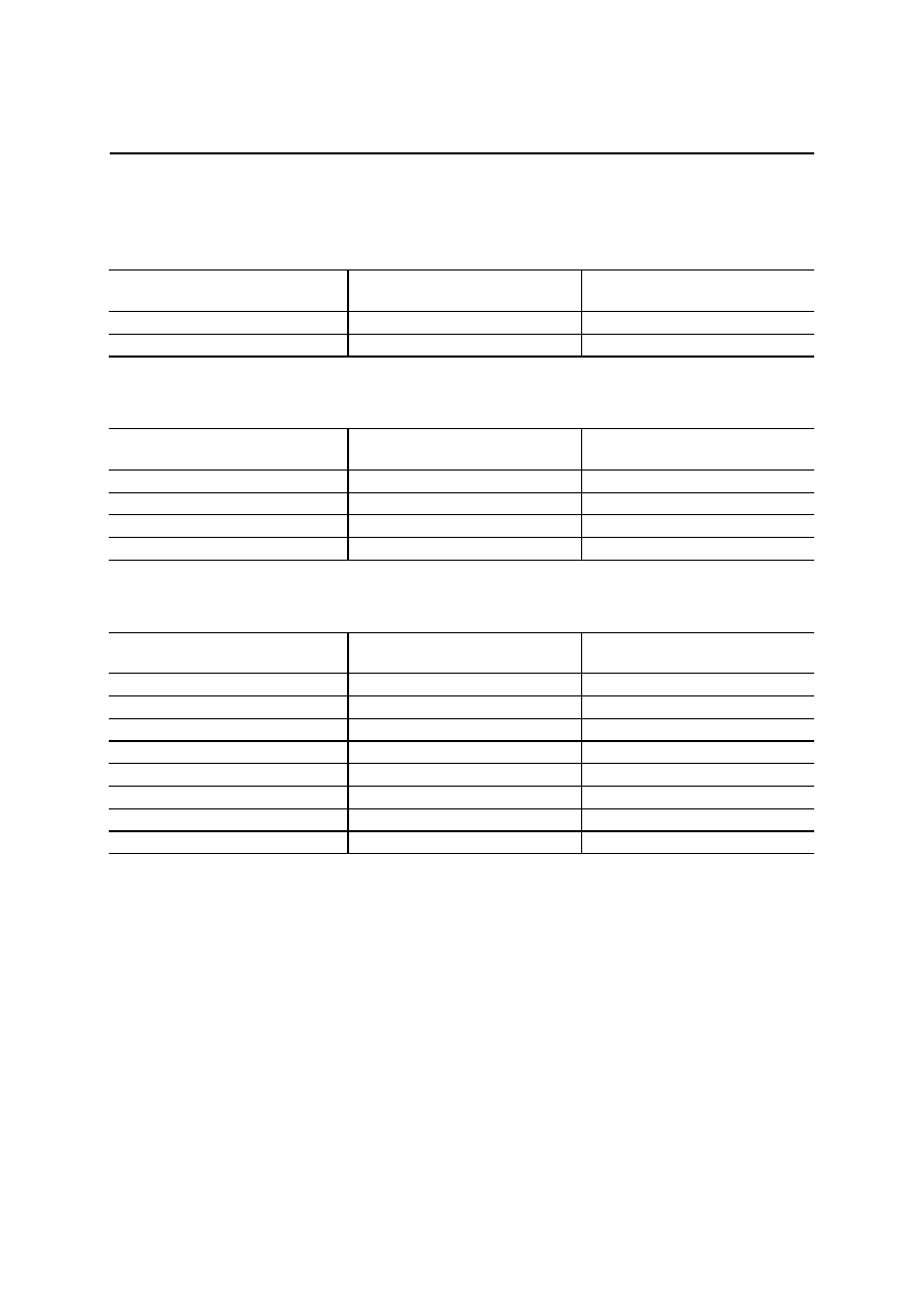
PRODUCT FAMILY
Family
Max. Operating Frequency
Access Time
Package
MS82V48540-7
143 MHz
5 ns
MS82V48540-8
125 MHz
6 ns
86-pin Plastic TSOP (II) (400 mil)

FEDS82V48540-01
OKI Semiconductor
MS82V48540
2/44
PIN CONFIGURATION (TOP VIEW)
86-Pin Plastic TSOP (II)
(Type K)
Pin Name
Function
Pin Name
Function
A0 � A10
Row Address Inputs
WE
Write Enable
A0 � A7
Column Address Inputs
DQM0 � DQM3
DQ Mask Enable
BA0, BA1
Bank Address
DQ0 � DQ31
Data Inputs/outputs
CLK
System Clock Input
V
CC
Supply
Voltage
CKE Clock
Enable
V
SS
Ground
CS
Chip Select
V
CC
Q
Supply Voltage for DQ
RAS
Row Address Strobe
V
SS
Q
Ground for DQ
CAS
Column Address Strobe
NC
No Connection
Note: The same power supply voltage must be provided to every V
CC
pin and V
CC
Q pin.
The same GND voltage level must be provided to every V
SS
pin and V
SS
Q pin.
10
11
12
13
9
8
7
6
5
4
3
2
1
14
15
16
17
18
19
20
21
22
23
24
25
26
27
28
29
30
31
32
33
34
35
36
37
38
39
40
41
42
43
77
76
75
74
78
79
80
81
82
83
84
85
86
73
72
71
70
69
68
67
66
65
64
63
62
61
60
59
58
57
56
55
54
53
52
51
50
49
48
47
46
45
44
V
CC
DQ0
V
CC
Q
DQ1
DQ2
V
SS
Q
DQ3
DQ4
V
CC
Q
DQ5
DQ6
V
SS
Q
DQ7
NC
V
CC
DQM0
WE
CAS
RAS
CS
NC
BA0
BA1
A10/AP
A0
A1
A2
DQM2
V
CC
NC
DQ16
V
SS
Q
DQ17
DQ18
V
CC
Q
DQ19
DQ20
V
SS
Q
DQ21
DQ22
V
CC
Q
DQ23
V
CC
V
SS
DQ15
V
SS
Q
DQ14
DQ13
V
CC
Q
DQ12
DQ11
V
SS
Q
DQ10
DQ9
V
CC
Q
DQ8
NC
V
SS
DQM1
NC
NC
CLK
CKE
A9
A8
A7
A6
A5
A4
A3
DQM3
V
SS
NC
DQ31
V
CC
Q
DQ30
DQ29
V
SS
Q
DQ28
DQ27
V
CC
Q
DQ26
DQ25
V
SS
Q
DQ24
V
SS
FEDS82V48540-01
OKI Semiconductor
MS82V48540
3/44
BLOCK DIAGRAM
Bank D
Bank C
Bank B
Timing
Register
DQ0
to
DQ31
RAS
CAS
A0 to
A10
BA0,
BA1
Bank
Controller
Internal
Column
Address
Counter
I/O
Controller
Column
Address
Buffers
Internal
Row
Address
Counter
Row
Address
Buffers
Read
Data
Register
Output
Buffers
Input
Data
Register
Input
Buffers
CKE
CLK
CS
WE
DQM0
to
DQM3
BA0, BA1
11
32
32 32
32
32
Bank A
Column Decoders
Sense Amplifiers
W
o
rd
Driv
e
r
s
12Mb
Memory
Cells
R
o
w
D
e
coder
s
8
FEDS82V48540-01
OKI Semiconductor
MS82V48540
4/44
PIN DESCRIPTION
CLK
Fetches all inputs at the "H" edge.
CS
Disables or enables device operation by asserting or deactivating all inputs except CLK, CKE,
DQM0, DQM1, DQM2 and DQM3.
CKE
Masks system clock to deactivate the subsequent CLK operation.
If CKE is deactivated, system clock will be masked so that the subsequent CLK operation is
deactivated. CKE should be asserted at least one cycle prior to a new command.
Address
Row & column multiplexed.
Row address: RA0 � RA10
Column address: CA0 � CA7
BA0, BA1
Selects bank to be activated during row address latch time and selects bank for precharge and
read/write during column address latch time.
BA0 = "L", BA1 = "L": Bank A
BA0 = "H", BA1 = "L": Bank B
BA0 = "L", BA1 = "H": Bank C
BA0 = "H", BA1 = "H": Bank D
RAS
CAS
WE
Functionality depends on the combination. For details, see the function truth table.
DQM0 �
DQM3
Masks the read data of two clocks later when DQM0 - DQM3 are set "H" at the "H" edge of the
clock signal.
Masks the write data of the same clock when DQM0 - DQM3 are set "H" at the "H" edge of the
clock signal.
DQM0 controls DQ0 to DQ7, DQM1 controls DQ8 to DQ15, DQM2 controls DQ16 to DQ23, and
DQM3 controls DQ24 to DQ31.
DQ0 � DQ31 Data inputs/outputs are multiplexed on the same pin.
*Notes: 1. When
CS
is set "High" at a clock transition from "Low" to "High", all inputs except CLK, CKE,
DQM0, DQM1, DQM2, and DQM3 are invalid.
2. When issuing an active, read or write command, the bank is selected by BA0 and BA1.
BA0
BA1
Active, read or write
0 0
Bank
A
1 0
Bank
B
0 1
Bank
C
1 1
Bank
D
3. The auto precharge function is enabled or disabled by the A10/AP input when the read or
write command is issued.
A10/AP BA0 BA1
Operation
0
0
0
After the end of burst, bank A holds the active status.
1
0
0
After the end of burst, bank A is precharged automatically.
0
1
0
After the end of burst, bank B holds the active status.
1
1
0
After the end of burst, bank B is precharged automatically.
0
0
1
After the end of burst, bank C holds the active status.
1
0
1
After the end of burst, bank C is precharged automatically.
0
1
1
After the end of burst, bank D holds the active status.
1
1
1
After the end of burst, bank D is precharged automatically.

FEDS82V48540-01
OKI Semiconductor
MS82V48540
5/44
4. When issuing a precharge command, the bank to be precharged is selected by the A10/AP,
BA0 and BA1 inputs.
A10/AP BA0 BA1
Operation
0
0
0
Bank A is precharged.
0
1
0
Bank B is precharged.
0
0
1
Bank C is precharged.
0
1
1
Bank D is precharged.
1
�
�
All banks are precharged.

FEDS82V48540-01
OKI Semiconductor
MS82V48540
6/44
COMMAND OPERATION
Mode Register Set Command (
CS, RAS, CAS, WE = "Low")
The MS82V48540 has the mode register that defines the operation mode "
CAS Latency, Burst Length, Burst
Sequence". The Mode Register Set command should be executed just after the MS82V48540 is powered on.
Before entering this command, all banks must be precharged. Next command can be issued after t
RSC
.
Auto Refresh Command (
CS, RAS, CAS = "Low", WE = "High")
The Auto Refresh command performs refresh automatically by the address counter. The refresh operation must be
performed 3,072 times within 64 ms and the next command can be issued after t
RC
from last Auto Refresh
command. Before entering this command, all banks must be precharged.
Self Refresh Entry/Exit Command (
CS, RAS, CAS, CKE = "Low", WE = "High")
The self refresh operation continues after the Self Refresh Entry command is entered, with CKE level left "low".
This operation terminates by making CKE level "high". The self refresh operation is performed automatically by
the internal address counter on the MS82V48540 chip.
In self refresh mode, no external refresh control is required. Before entering self refresh mode, all banks must be
precharged. Next command can be issued after t
RC
.
Single Bank Precharge Command (
CS, RAS, WE, A10/AP = "Low", CAS = "High")
The Single Bank Precharge command triggers bank precharge operation. Precharge bank is selected by BA0 and
BA1.
All Banks Precharge Command (
CS, RAS, WE = "Low", CAS, A10/AP = "High")
The All Bank Precharge command triggers precharge of all banks.
If this command is executed during special bank active mode, the special bank active mode is terminated.
Bank Active Command (
CS, RAS = "Low", CAS, WE = "High")
The Bank Active command activates the bank selected by BA0 and BA1. The Bank Active command corresponds
to conventional DRAM's
RAS falling operation. Row addresses "A0 � A10, BA0 and BA1" are strobed.
Write Command (
CS, CAS, WE, A10/AP = "Low", RAS = "High")
The Write command is required to begin burst write operation. Then burst access initial bit column address is
strobed.
Write with Auto Precharge Command (
CS, CAS, WE = "Low", RAS, A10/AP = "High")
The Write with Auto Precharge command is required to begin burst write operation with automatic precharge after
the burst write. Any command that interrupts this operation cannot be issued.
Read Command (
CS, CAS, A10/AP = "Low", RAS, WE = "High")
The Read command is required to begin burst read operation. Then burst access initial bit column address is
strobed.

FEDS82V48540-01
OKI Semiconductor
MS82V48540
7/44
Read with Auto Prechaege Command (
CS, CAS = "Low", RAS, WE, A10/AP = "High")
The Read with Auto Precharge command is required to begin burst read operation with auto precharge after the
burst read. Any command that interrupts this operation cannot be issued.
No Operation Command (
CS = "Low", RAS, CAS, WE = "High")
The No Operation command does not trigger any operation.
Device Deselect Command (
CS = "High")
The Device Deselect command disables the
RAS, CAS, WE and Address input. This command does not trigger
any operation.
Data Write/Output Enable Command (DQMi = "Low")
The Data Write/Output Enable command enables DQ0 - DQ31 in read or write.
The each DQM0, 1, 2 and 3 corresponds to DQ0 - DQ7, DQ8 - DQ15, DQ16 - DQ23 and DQ24 - DQ31
respectively.
Data Mask/Output Disable Command (DQMi = "High")
The Data Mask/Output Disable command disables DQ0 - DQ31 in read or write. In read cycle output buffers are
disabled after 2 clocks . In write cycle input buffers are disabled at the same clock. The each DQM0, 1, 2 and 3
corresponds to DQ0 - DQ7, DQ8 - DQ15, DQ16 - DQ23 and DQ24 - DQ31
respectively.
Burst Stop Command (
CS, WE = "Low", RAS, CAS = "High")
The Burst Stop command stops burst access. After the Burst Stop command is entered, the output buffer goes into
high impedance state.
FEDS82V48540-01
OKI Semiconductor
MS82V48540
8/44
SPECIAL READ/WRITE OPERATION
The special read or write operation is activated by executing the Read or Write command after selecting the special
page mode with the Mode Register command.
The automatic bank switching and automatic row address increment operations are activated by executing the
Bank Active command during Special Page mode, and the serial access starts from the address fetched with the
Read or Write command. The burst operation starts from the start address toward the column. When the last
column address is reached, the bank is automatically switched and the row address is also automatically
incremented and the serial access continues from the start column address. The automatic bank switching and
automatic row address increment operations continue until the All Bank Precharge command is executed each time
the last column address is reached.
Since the bank switching and row address increment are automatically made during the special read or write
operation, the row address proceeds as shown in the following figure.
Row
Column
Start
address
Note) The circled numbers indicate the orders of row address increment.
0
1535
Operation is ended by input of
All Bank Precharge command.
0
1535
3071
3072
0
256
0 1535
0
1535
0
256
Bank A
BA0 = "L", BA1 = "L"
Bank C
BA0 = "L", BA1 = "H"
Bank B
BA0 = "H", BA1 = "L"
Bank D
BA0 = "H", BA1 = "H"
3073 3075
3174 3076 3078 3080
3077 3079
6144
6143
0
256
0
256
FEDS82V48540-01
OKI Semiconductor
MS82V48540
9/44
TRUTH TABLE
Command Truth Table
Address
Function
CS RAS CAS WE
BA0, 1
A10/AP
A9 � A0
Device Deselect
H
�
�
�
�
�
�
No Operation
L
H
H
H
�
�
�
Mode Register Set
L
L
L
L
OP. CODE
Auto Refresh
L
L
L
H
�
�
�
Bank Activate
L
L
H
H
BA
RA
Read
L H L H BA L
CA
(A7
�
A0)
Read with Auto Precharge
L
H
L
H
BA
H
CA (A7 � A0)
Write
L
H
L
L
BA
L
CA (A7 � A0)
Write with Auto Precharge
L
H
L
L
BA
H
CA (A7 � A0)
Precharge Select Bank
L
L
H
L
BA
L
�
Precharge All Banks
L
L
H
L
�
H
�
Burst Stop
L
H
H
L
�
�
�
DQM Truth Table
Function DQMi
Data Write/Output Enable
L
Data Mask/Output Disable
H
FEDS82V48540-01
OKI Semiconductor
MS82V48540
10/44
Function Truth Table (1/3)
Note 1
Current State
CS RAS CAS WE
BA Address
Action
Note
H
�
�
�
�
�
NOP
L H H H
�
�
NOP
L H H L BA
�
ILLEGAL 2
L H L
�
BA CA,
A10 ILLEGAL
2
L L H H BA RA Row
Active
L L L L L
Op-Code
Mode
Register
Write
L L H L BA A10 NOP
4
Idle
L L L H
�
�
Auto Refresh/Self refresh
5
H
�
�
�
�
�
NOP
L H H
�
�
�
NOP
L H L H BA
CA,
A10
Read
L H L L BA
CA,
A10
Write
L L H H BA RA ILLEGAL
2
L L H L BA A10 Precharge
Active (ACT)
L L L
�
�
�
ILLEGAL
H
�
�
�
�
�
NOP
L H H
�
�
�
NOP
L H L H BA CA Serial
Read
L H L L BA CA Serial
Write
L L H H BA RA ILLEGAL
L L H L BA
A10:
L
ILLEGAL
L L H L BA
A10:
H
Precharge
Active (Special
Page Mode)
(SACT)
L L L
�
�
�
ILLEGAL
H
�
�
�
�
�
NOP (Continue Row Active after Burst ends)
L H H H
�
�
NOP (Continue Row Active after Burst ends)
L H H L
�
�
Burst Stop
Row Active
L
H
L
H
BA CA, A10 Term Burst, new Read
3
L
H
L
L
BA CA, A10 Term Burst, start Write
3
L L H H BA RA ILLEGAL
2
L
L
H
L
BA
A10
Term Burst, execute Precharge
Read (RD)
L L L
�
�
�
ILLEGAL
H
�
�
�
�
�
NOP (Continue Row Active after Burst ends)
L H H H
�
�
NOP (Continue Row Active after Burst ends)
L H H L
�
�
Burst Stop
Row Active
L
H
L
H
BA CA, A10 Term Burst, start Read
3
L
H
L
L
BA CA, A10 Term Burst, new Write
3
L L H H BA RA ILLEGAL
2
L
L
H
L
BA
A10
Term Burst, execute Precharge
3
Write (WT)
L L L
�
�
�
ILLEGAL
FEDS82V48540-01
OKI Semiconductor
MS82V48540
11/44
Function Truth Table (2/3)
Note 1
Current State
CS RAS CAS WE
BA Address
Action
Note
H
�
�
�
�
�
NOP (Continue Burst to End and enter Precharge)
L H H H
�
�
NOP (Continue Burst to End and enter Precharge)
L H H L
�
�
ILLEGAL
L H L H BA
CA,
A10
ILLEGAL
L H L L BA
CA,
A10
ILLEGAL
L L H H BA RA ILLEGAL
2
L L H L BA A10 ILLEGAL
2
Read with Auto
Precharge
(RAP)
L L L
�
�
�
ILLEGAL
H
�
�
�
�
�
NOP (Continue Burst to End and enter Precharge)
L H H H
�
�
NOP (Continue Burst to End and enter Precharge)
L H H L
�
�
ILLEGAL
L H L H BA
CA,
A10
ILLEGAL
L H L L BA
CA,
A10
ILLEGAL
L L H H BA RA ILLEGAL
2
L L H L BA A10 ILLEGAL
2
Write with Auto
Precharge
(WAP)
L L L
�
�
�
ILLEGAL
H
�
�
�
�
�
NOP (Continue serial read)
L H H H
�
�
NOP (Continue serial read)
L H H L
�
�
ILLEGAL
L H L
�
BA CA ILLEGAL
L L H H BA RA ILLEGAL
L L H L BA
A10:
L
ILLEGAL
L L H L BA
A10:
H
Precharging
Read (Special
Page Mode)
(SRD)
L L L
�
�
�
ILLEGAL
H
�
�
�
�
�
NOP (Continue serial write)
L H H H
�
�
NOP (Continue serial write)
L H H L
�
�
ILLEGAL
L H L
�
BA CA ILLEGAL
L L H H BA RA ILLEGAL
L L H L BA
A10:
L
ILLEGAL
L L H L BA
A10:
H
Precharging
Write (Special
Page Mode)
(SWT)
L L L
�
�
�
ILLEGAL
H
�
�
�
�
�
NOP
Idle after t
RP
L H H H
�
�
NOP
Idle after t
RP
L H H L BA
�
ILLEGAL 2
L H L
�
BA CA ILLEGAL
2
L L H H BA RA ILLEGAL
2
L L H L BA A10 NOP
4
Precharging
(PRE)
L L L
�
�
�
ILLEGAL

FEDS82V48540-01
OKI Semiconductor
MS82V48540
12/44
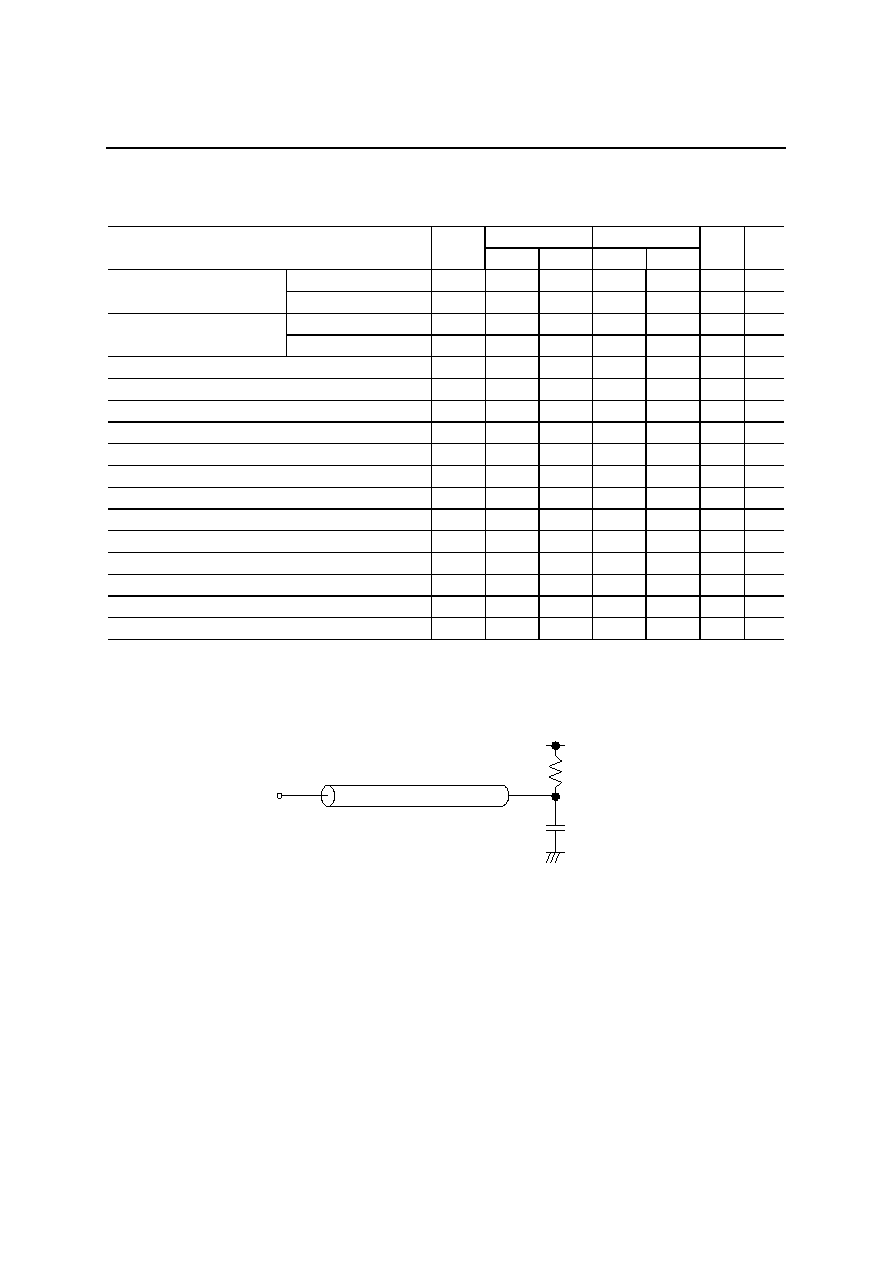
Function Truth Table (3/3)
Note 1
Current State
CS RAS CAS WE
BA Address
Action
Note
H
�
�
�
�
�
NOP
Idle after t
RC
L H H H
�
�
NOP
Idle after t
RC
L H H L BA
�
ILLEGAL
L H L
�
BA CA ILLEGAL
L L H H BA RA ILLEGAL
L L H L BA A10 ILLEGAL
Refreshing
(REF)
L L L
�
�
�
ILLEGAL
ABBREVIATIONS
BA = Bank Address
RA = Row Address
CA = Column Address
NOP = No Operation command
Notes: 1. All inputs are enabled when CKE is set high for at least 1 cycle prior to the inputs.
2. Illegal to bank in specified state, but may be legal in some cases depending on the state of
bank selection.
3. To avoid bus contention, satisfy t
CCD
and t
DPL
.
4. NOP to bank precharging or in idle state. Precharges activated bank by BA or A10/AP.
5. Illegal if any bank is not idle.
FEDS82V48540-01
OKI Semiconductor
MS82V48540
13/44
Function Truth Table for CKE
Current State (n) CKEn-1 CKEn
CS RAS CAS WE
Address Action Note
H
�
�
�
�
�
�
INVALID
L H
H
�
�
�
�
Exit Self Refresh
ABI
L H L H H H
�
Exit Self Refresh
ABI
L H
L
H
H
L
�
ILLEGAL
L H
L
H
L
�
�
ILLEGAL
L H
L
L
�
�
�
ILLEGAL
Self Refresh
(SREF)
L L
�
�
�
�
�
NOP (Maintain Self Refresh)
H
�
�
�
�
�
�
INVALID
L H
H
�
�
�
�
Exit Self Refresh
ABI
L H L H H H
�
Exit Self Refresh
ABI
L H
L
H
H
L
�
ILLEGAL
L H
L
H
L
�
�
ILLEGAL
L H
L
L
�
�
�
ILLEGAL
Power Down (PD)
L L
�
�
�
�
�
NOP (Continue power down mode)
H H
�
�
�
�
�
Refer to Truth Table
6
H L
H
�
�
�
�
Enter Power Down
6
H L L H H H
�
Enter Power Down
6
H L L
H
H
L
�
ILLEGAL 6
H L L
H
L
�
�
ILLEGAL 6
H L L
L
H
L
�
ILLEGAL 6
H L L L L H
�
Enter Self Refresh
6
H L L L L L
�
ILLEGAL 6
All Banks Idle
(ABI)
L L
�
�
�
�
�
NOP 6
H H
�
�
�
�
�
Refer to Truth Table
H L
�
�
�
�
�
Begin Clock Suspend Next Cycle
L H
�
�
�
�
�
Enable Clock of Next Cycle
Any State Other
than Listed Above
L L
�
�
�
�
�
Continue Clock Suspension
Note: 6. Power-down and self refresh can be entered only when all the banks are in an idle state.

FEDS82V48540-01
OKI Semiconductor
MS82V48540
14/44
Mode Set Address Keys
Operation Code
CAS
Latency
Burst Type
Burst Length
A8 A7
TM
A6 A5 A4
CL
A3
BT
A2 A1 A0
BT
=
0
BT
=
1
0 0 Mode
Setting 0 0 0 Reserved 0 Sequential 0 0 0
1
Reserved
0 1
0 0 1 Reserved 1 Interleave 0 0 1
2
Reserved
1 0
0 1 0
2
0 1 0
4
4
1 1
Vender
Use
Only
0 1 1
3
0 1 1
8
8
Write Burst Length
*Note 1
1 0 0 Reserved
1 0 0 Reserved Reserved
A9
Length
1 0 1 Reserved
1 0 1 Reserved Reserved
0
Burst
1 1 0 Reserved
1 1 0 Special
page Reserved
1 Single
Bit 1
1
1
Reserved
1 1 1 Full
Page Reserved
*Note 1: To select Special Page mode, set A9 to "L".
The write burst length during Special Page mode is set only for Burst.
POWER ON SEQUENCE
1. With CKE = "H", DQM = "H" and the other inputs in NOP state, turn on the power supply and
start the system clock.
2. After the V
CC
voltage has reached the specified level, pause for 200
�
s or more with the input
kept in NOP state.
3. Issue the precharge all bank command.
4. Apply an Auto-refresh 8 or more times.
5. Enter the mode register command.
FEDS82V48540-01
OKI Semiconductor
MS82V48540
15/44
Burst Length and Sequence
BL = 2
Starting Address
(column address A0, binary)
Sequential Type
Interleave Type
0
0, 1
Not supported
1
1, 0
Not supported
BL = 4
Starting Address
(column address A1, A0, binary)
Sequential Type
Interleave Type
00
0, 1, 2, 3
0, 1, 2, 3
01
1, 2, 3, 0
1, 0, 3, 2
10
2, 3, 0, 1
2, 3, 0, 1
11
3, 0, 1, 2
3, 2, 1, 0
BL = 8
Starting Address
(column address A2 - A0, binary)
Sequential Type
Interleave Type
000
0, 1, 2, 3, 4, 5, 6, 7
0, 1, 2, 3, 4, 5, 6, 7
001
1, 2, 3, 4, 5, 6, 7, 0
1, 0, 3, 2, 5, 4, 7, 6
010
2, 3, 4, 5, 6, 7, 0, 1
2, 3, 0, 1, 6, 7, 4, 5
011
3, 4, 5, 6, 7, 0, 1, 2
3, 2, 1, 0, 7, 6, 5, 4
100
4, 5, 6, 7, 0, 1, 2, 3
4, 5, 6, 7, 0, 1, 2, 3
101
5, 6, 7, 0, 1, 2, 3, 4
5, 4, 7, 6, 1, 0, 3, 2
110
6, 7, 0, 1, 2, 3, 4, 5
6, 7, 4, 5, 2, 3, 0, 1
111
7, 0, 1, 2, 3, 4, 5, 6
7, 6, 5, 4, 3, 2, 1, 0
BL = Special, Full : Sequential only
FEDS82V48540-01
OKI Semiconductor
MS82V48540
16/44
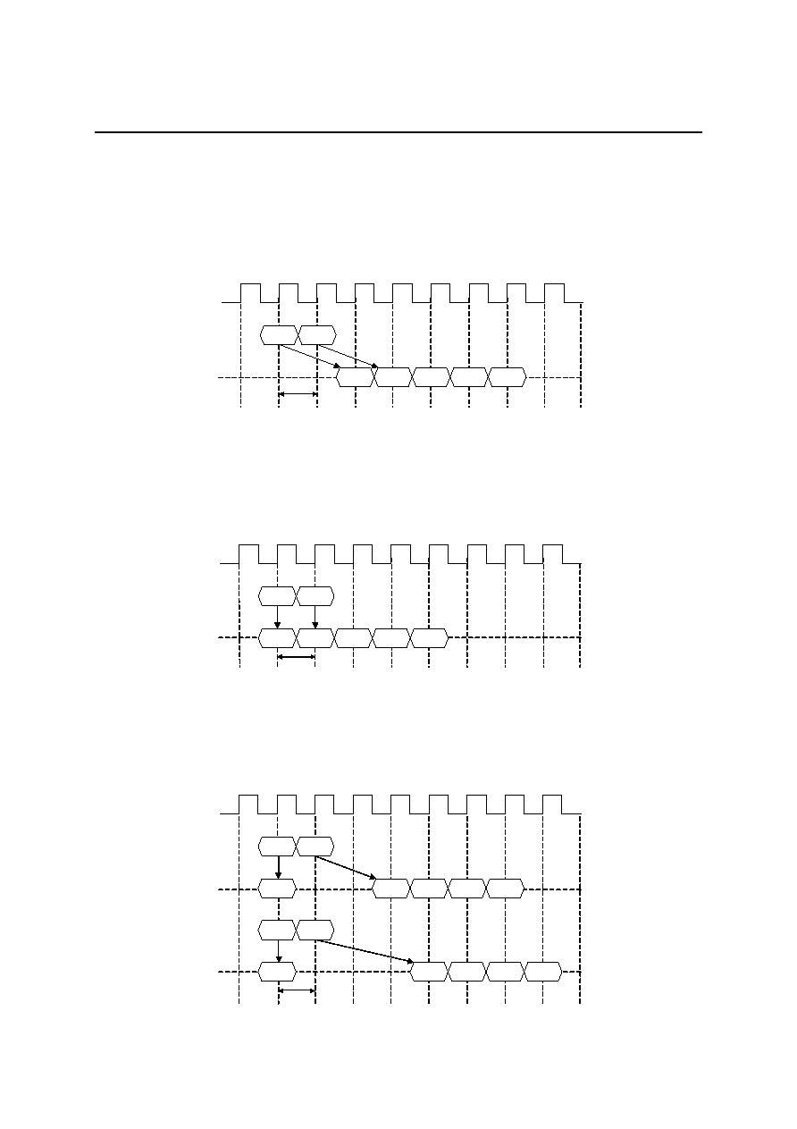
READ/WRITE COMMAND INTERVAL
Read to Read Command Interval
Write to Write Command Interval
Write to Read Command Interval
CLK
RD-A
DQ
QB1
0 1 2 3 4 5 6 7 8
QB2 QB3
QA1
RD-B
QB4
1cycle
BL = 4, CL = 2
Hi-Z
CLK
WT-A
DQ
DA1
0 1 2 3 4 5 6 7 8
DB1 DB2 DB3
WT-B
DB4
1cycle
BL = 4, CL = 2
Hi-Z
CLK
WT-A
DQ
DA1
0 1 2 3 4 5 6 7 8
QB1 QB2 QB3
RD-B
QB4
Hi-Z
BL = 4
CL = 2
WT-A
DQ
DA1
QB1 QB2 QB3
RD-B
QB4
Hi-Z
1cycle
CL = 3
FEDS82V48540-01
OKI Semiconductor
MS82V48540
17/44
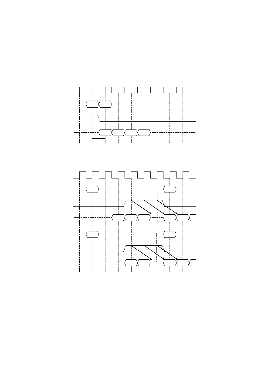
Read to Write Command Interval
CLK
DQ
0 1 2 3 4 5 6 7 8
DB1 DB2 DB3
RD-A WT-B
DQM
DB4
Hi-Z
1cycle
BL = 4, CL = 2, 3
CL = 2, 3
CLK
DQ
0 1 2 3 4 5 6 7 8
QA2 QA3
RD-A
WT-B
DQM
DB1 DB2
Hi-Z
CL = 2
BL = 4, CL = 2, 3
DQ
QA1 QA2
RD-A
WT-B
DQM
DB1 DB2
Hi-Z
CL = 3
QA1
Hi-Z is
necessary
Hi-Z is
necessary

FEDS82V48540-01
OKI Semiconductor
MS82V48540
18/44
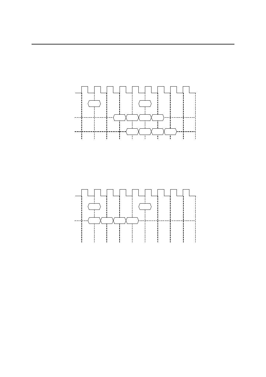
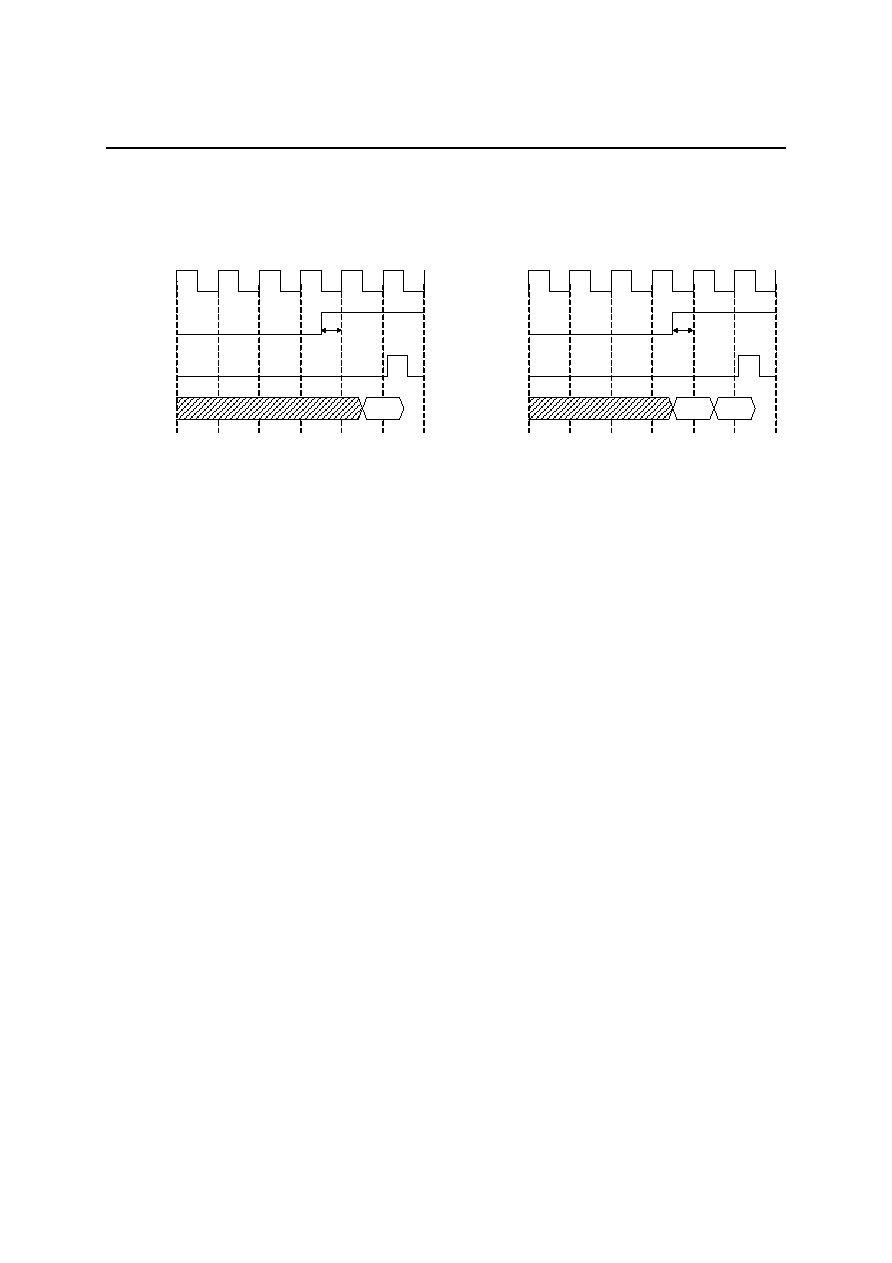
BURST TERMINATION
Burst Read Termination by Precharging in READ Cycle
Burst Read Termination by Precharging in WRITE Cycle
Note: D5 data will not be written
CLK
CL = 2
RD
DQ
Q1
0 1 2 3 4 5 6 7 8
PRE
CL = 3
RD
DQ
PRE
Q2
Q3
Q4
Q1
Q2
Q3
Q4
Hi-Z
Hi-Z
BL = 2, 4, 8, Full
ACT
ACT
t
RP
t
RP
CLK
CL = 2
WT
DQ
D1
0 1 2 3 4 5 6 7 8
PRE
CL = 3
WT
DQ
PRE
D2
D3
D4
D1
D2
D3
D4
Hi-Z
Hi-Z
BL = 2, 4, 8, Full
ACT
ACT
D5
t
RP
t
RP
D5
FEDS82V48540-01
OKI Semiconductor
MS82V48540
19/44
Read Burst Stop Command
Write Burst Stop Command
CLK
CL = 2
RD
DQ
Q2
0 1 2 3 4 5 6 7 8
BST
CL = 3
DQ
Q3
Q4
Q2
Q3
Q4
Hi-Z
Hi-Z
BL = 2, 4, 8, Full
Q1
Q1
CLK
CL = 2, 3
WT
DQ
D1
0 1 2 3 4 5 6 7 8
BST
D2
D3
Hi-Z
BL = 2, 4, 8, Full
D4
FEDS82V48540-01
OKI Semiconductor
MS82V48540
20/44
AUTO PRECHARGE
Read with Auto Precharge
Write with Auto Precharge
CLK
RAP
DQ
0 1 2 3 4 5 6 7 8
Q1
Q2
Q3
Q4
Hi-Z
BL = 4
CL = 2
DQ
Q1
Q2
Q3
Q4
Hi-Z
CL = 3
RAP
Auto precharge starts
Auto precharge starts
(t
RAS
is satisfied)
CLK
WAP
DQ
0 1 2 3 4 5 6 7 8
D1
D2
D3
D4
Hi-Z
BL = 4
CL = 2
DQ
D1
D2
D3
D4
Hi-Z
CL = 3
WAP
Auto precharge starts
Auto precharge starts
(t
RAS
is satisfied)
FEDS82V48540-01
OKI Semiconductor
MS82V48540
21/44
ELECTRICAL CHARACTERISTICS
Absolute Maximum Ratings
Parameter Symbol
Rating
Unit
Voltage on Power Supply Pin Relative to GND
V
CC
�0.5 to 4.6
V
Voltage on Input Pin Relative to GND
V
IN
, V
OUT
�0.5 to V
CC
+ 0.5
4.6
V
Short Circuit Output Current
I
OS
50 mA
Power Dissipation
P
D
* 1 W
Operating Temperature
T
opr
0 to 70
�C
Storage Temperature
T
stg
�55 to 150
�C
*: Ta = 25 �C
Recommended Operating Conditions
(Ta = 0 to 70�C)
Parameter Symbol
Min.
Typ.
Max.
Unit
V
CC
3.0 3.3 3.6 V
Power Supply Voltage
V
SS
0 0 0 V
Input High Voltage
V
IH
2.0 --
V
CC
+ 0.3
V
Input Low Voltage
V
IL
�0.3 -- 0.8 V
Capacitance
(V
CC
= 3.3 V �0.3 V, Ta = 25�C, f = 1 MHz)
Parameter Symbol
Min.
Max.
Unit
Input Capacitance (A0 � A10, BA0, BA1)
C
IN1
-- 5 pF
Input Capacitance
(CLK, CKE,
CS
,
RAS
,
CAS
,
WE
DQM 0 � DQM3)
C
IN2
-- 5 pF
Output Capacitance
(DQ0 � DQ31)
C
OUT
-- 6 pF
FEDS82V48540-01
OKI Semiconductor
MS82V48540
22/44
DC Characteristics
Test Condition
MS82V48540-7 MS82V48540-8
Parameter Symbol
CKE Other
Min.
Max.
Min.
Max.
Unit Note
Output High Voltage
V
OH
--
I
OH
= �2.0 mA 2.4
--
2.4
--
V
Output Low Voltage
V
OL
-- I
OL
= 2.0 mA
--
0.4
--
0.4
V
Input Leakage Current
I
LI
--
-- �10
10
�10
10
�
A
Output Leakage Current
I
LO
--
-- �10
10
�10
10
�
A
Operating Current
(1 Bank)
I
CC1
CKE
V
IH
t
CK
= t
CK
min.
t
RC
= t
RC
min.
No Burst
-- 200 -- 180 mA 1,
2
I
CC2P
CKE
V
IL
t
CK
= t
CK
min.
--
2
--
2
mA
Precharge Standby Current
in Power Down Mode
I
CC2PS
CKE
V
IL
CLK
V
IL
t
CK
=
-- 2 -- 2 mA
I
CC2N
CKE
V
IH
CS
V
IH
t
CK
= t
CK
min.
-- 40 -- 40 mA
Precharge Standby Current
in Non Power Down Mode
I
CC2NS
CKE
V
IH
CLK
V
IL
t
CK
=
-- 20 -- 20 mA
I
CC3P
CKE
V
IL
t
CK
= t
CK
min.
--
3
--
3
mA
Active Standby Current in
Power Down Mode
I
CC3PS
CKE
V
IL
CLK
V
IL
t
CK
=
-- 3 -- 3 mA
I
CC3N
CKE
V
IH
CS
V
IH
t
CK
= t
CK
min.
-- 50 -- 50 mA
Active Standby Current in
Non Power Down Mode
I
CC3NS
CKE
V
IH
CLK
V
IL
t
CK
=
-- 30 -- 30 mA
Operating Current
(Burst Mode)
I
CC4
CKE
V
IH
t
CK
= t
CK
min.
--
240
--
200
mA
1, 2
Refresh Current
I
CC5
CKE
V
IH
t
RC
t
RC
min.
--
200
--
180
mA
Self Refresh Current
I
CC6
CKE
0.2V
-- --
3
--
3
mA
Notes 1. The maximum value of power supply current is obtained with the output open.
2. Address and data are changed only one time during one cycle.
FEDS82V48540-01
OKI Semiconductor
MS82V48540
23/44
AC Characteristics
Test conditions
� AC measurements assume t
T
= 1 ns.
� Reference level for measuring timing of input signals is 1.4 V. Transition times are measured between V
IH
and
V
IL
.
� If t
T
is longer than 1 ns, reference level for measuring timing of input signals is V
IH (MIN.)
and V
IL (MAX)
.
� An access time is measured at 1.4 V.
� Input levels at the AC testing are 2.4 V/0.4 V.
t
CK
t
CH
t
CL
t
Setup
t
Hold
t
OH
CLK
Input
Output
2.4 V
1.4 V
0.4 V
2.4 V
1.4 V
0.4 V
1.4 V
1.4 V
t
AC
FEDS82V48540-01
OKI Semiconductor
MS82V48540
24/44
Synchronous Characteristics
MS82V48540-7 MS82V48540-8
Parameter Symbol
Min. Max. Min. Max.
Unit Note
CAS
Latency = 3
t
CK3
7 -- 8 -- ns
Clock Cycle Time
CAS
Latency = 2
t
CK2
12 -- 12 -- ns
CAS
Latency = 3
t
AC3
-- 5 -- 6 ns
1
Access Time from CLK
CAS
Latency = 2
t
AC2
-- 8 -- 8 ns
1
CLK High Level Width
t
CH
2.5 -- 3 -- ns
CLK Low Level Width
t
CL
2.5 -- 3 -- ns
Data-out Hold Time
t
OH
2 -- 2 -- ns
Data-out Low-impedance Time
t
LZ
0 -- 0 -- ns
Data-out High-impedance Time
t
HZ
-- 5 -- 6 ns
Data-in Setup Time
t
DS
2 -- 2 -- ns
Data-in Hold Time
t
DH
1 -- 1 -- ns
Address Setup Time
t
AS
2 -- 2 -- ns
Address Hold Time
t
AH
1 -- 1 -- ns
CKE Setup Time
t
CKS
2 -- 2 -- ns
CKE Hold Time
t
CKH
1 -- 1 -- ns
Command (
CS
,
RAS
,
CAS
,
WE
, DQM) Setup Time
t
CMS
2 -- 2 -- ns
Command (
CS
,
RAS
,
CAS
,
WE
, DQM) Hold Time
t
CMH
1 -- 1 -- ns
Note 1. Output load.
Z = 50
1.4 V
Output
30 pF
50

FEDS82V48540-01
OKI Semiconductor
MS82V48540
25/44
Asynchronous Characteristics
Parameter
MS82V48540-7 MS82V48540-8
Symbol
Min. Max. Min. Max.
Unit Note
REF to REF/ACT/SACT Command Period
t
RC
63 -- 72 -- ns
ACT to PRE Command Period
t
RAS
42 120k 48 120k
ns
SACT to PRE Command Period
t
RASS
6 -- 6 --
CLK
PRE to ACT Command Period
t
RP
21 -- 24 -- ns
PRE-ALL (Special Page) to SACT Command Period
t
RPS
9 -- 9 --
CLK
Delay Time ACT/SACT to READ/WRITE Command
t
RCD
21 -- 24 -- ns
ACT (0) to ACT (1) Command Period
t
RRD
14 -- 16 -- ns
READ/WRITE to READ/WRITE Command Period
t
CCD
7 -- 8 -- ns
Data-in to PRE Command Period
t
DPL
7 -- 8 -- ns
Data Output to WRITE Command Input Time
t
OWD
14 -- 16 -- ns
Mode Register Set Cycle Time
t
RSC
14 -- 16 -- ns
Transition Time
t
T
1 30 1 30 ns
Refresh Time
t
REF
-- 64 -- 64 ms

FEDS82V48540-01
OKI Semiconductor
MS82V48540
26/44
TIMING WAVEFORM
READ/WRITE CYCLE (BL = 2, CL = 3)
CLK
0 1 2 3 4 5 6 7 8 9 10
11 12 13 14 15 16 17 18 19
CKE
CS
CAS
WE
BA0
ADD
A10
/AP
DQM
0 - 3
DQ
t
CK
t
CH
t
CL
t
CMS
t
CMH
t
CKS
t
AS
t
AH
RAa
t
CMS
t
CMH
t
AC
t
OH
t
HZ
t
LZ
t
DS
t
DH
CAa
RAa
CAb
DAb1 DAb2
RDa
RDa
QAa1 QAa2
t
CKH
Hi-Z
t
RCD
t
RAS
t
RC
t
DPL
t
RP
ACT-A RD-A
WT-A PRE-A ACT-D
RAS
t
OWD
BA1
FEDS82V48540-01
OKI Semiconductor
MS82V48540
27/44
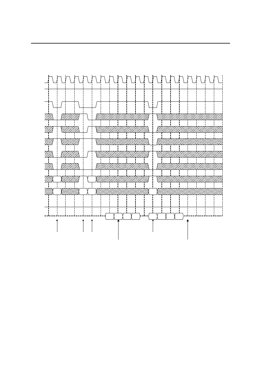
Special READ CYCLE (BL = Special Page, CL = 3)
RAa
CAa
RAa
QAa4
RDa
RDa
Hi-Z
t
RCD
t
RASS
t
RPS
SACT-A
SRD-A
Special Read Start
PRE-ALL
SACT-D
L
H
Qn-1
Qn
Qn+1 Qn+2
QAa1 QAa2 QAa3
0 1 2 3 4 5 6 7 8 9 10
11 12
13 14
15 16 17 18 19
CLK
CKE
CS
CAS
WE
BA0
ADD
A10
/AP
DQM
0 - 3
DQ
RAS
BA1
FEDS82V48540-01
OKI Semiconductor
MS82V48540
28/44
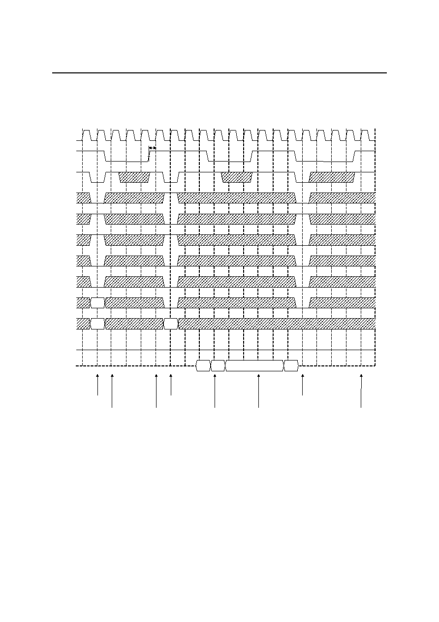
Special WRITE CYCLE (BL = Special Page, CL = 3)
RAa
CAa
RAa
DAa4
RBa
RBa
Hi-Z
t
RCD
t
RASS
t
RPS
SACT-A
SWT-A
Special Write Start
PRE-ALL
SACT-B
L
H
DAa5
Dn-2
Dn-1
Dn
DAa1 DAa2
DAa3
t
DPL
0 1 2 3 4 5 6 7 8 9 10
11 12
13 14
15 16 17 18 19
CLK
CKE
CS
CAS
WE
BA0
ADD
A10
/AP
DQM
0 - 3
DQ
RAS
BA1
FEDS82V48540-01
OKI Semiconductor
MS82V48540
29/44
Mode Register Set
Hi-Z
PRE-ALL
H
MRA
ACT
t
RSC
t
RP
0 1 2 3 4 5 6 7 8 9 10
11 12 13 14 15 16 17 18 19
CLK
CKE
CS
CAS
WE
BA
ADD
A10
/AP
DQM
0 - 3
DQ
RAS

FEDS82V48540-01
OKI Semiconductor
MS82V48540
30/44
Auto Reflesh
Hi-Z
t
RC
PRE-ALL
L
H
REF
REF
ACT
t
RC
t
RP
0 1 2 3 4 5 6 7 8 9 10
11 12 13 14 15 16 17 18 19
CLK
CKE
CS
CAS
WE
BA
ADD
A10
/AP
DQM
0 - 3
DQ
RAS

FEDS82V48540-01
OKI Semiconductor
MS82V48540
31/44
Self Reflesh (Entry and Exit)
Hi-Z
t
RC
PRE-ALL
L
H
SELF
Entry
ACT
t
RC
t
RP
SELF
Exit
SELF
Entry
SELF
Exit
0 1 2 3 4 5 6 7 8 9 10
11 12
13 14
15 16 17 18 19
CLK
CKE
CS
CAS
WE
BA
ADD
A10
/AP
DQM
0 - 3
DQ
RAS

FEDS82V48540-01
OKI Semiconductor
MS82V48540
32/44
Burst Termination by Precharging (BL = 8, CL = 3)
Hi-Z
ACT-A
L
H
WT-A
PRE Command
Termination
RAa
CAa
RAa
RAb
RAb
PRE-A
DAa1 DAa2
QAb1
QAb2
QAb3
QAb4
CAb
RD-A
ACT-A
PRE-A
PRE Command
Termination
0 1 2 3 4 5 6 7 8 9 10
11 12 13 14 15 16 17 18 19
CLK
CKE
CS
CAS
WE
BA0
ADD
A10
/AP
DQM
0 - 3
DQ
RAS
BA1
FEDS82V48540-01
OKI Semiconductor
MS82V48540
33/44
Auto Precharging (BL = 4, CL = 3)
Hi-Z
ACT-A
L
H
RAP-A
AP-A
RAa
CAa
RAa
RBa
RBa
ACT-B
QAa1
QAa2
QAa3
QAa4
DBa1
DBa2
DBa3
DBa4
CBa
AP-B
WAP-B
0 1 2 3 4 5 6 7 8 9 10
11 12
13 14
15 16 17 18 19
CLK
CKE
CS
CAS
WE
BA0
ADD
A10
/AP
DQM
0 - 3
DQ
RAS
BA1
FEDS82V48540-01
OKI Semiconductor
MS82V48540
34/44
Power Down Mode and Clock Suspension (BL = 4, CL = 2)
Hi-Z
ACT-A
L
PD
Entry
PD
Exit
Clock
Mask Start
PRE-A
RAa
RAa
CAa
ACTIVE STANDBY
RD-A
QAa2
QAa3
QAa4
Clock
Mask End
PD
Entry
PD
Exit
PRECHARGE STANDBY
t
CKS
QAa1
0 1 2 3 4 5 6 7 8 9 10
11 12
13 14
15 16 17 18 19
CLK
CKE
CS
CAS
WE
BA0
ADD
A10
/AP
DQM
0 - 3
DQ
RAS
BA1
FEDS82V48540-01
OKI Semiconductor
MS82V48540
35/44
CLOCK Suspend Exit & Power Down Exit
1) Clock Suspend (= Active Power Down) Exit
2) Power Down (= Precharge Power Down) Exit
Notes: 1. Active power down: one or both bank active state.
2. Precharge power down: both bank precharge state.
3. NOP should be issued. And new command can be issued after 1 Clock.
CLK
Internal
CLK
Command
RD
CKE
t
CKS
Note 1
CLK
ACT
CKE
t
CKS
Note 3
NOP
Internal
CLK
Command
Note 2
FEDS82V48540-01
OKI Semiconductor
MS82V48540
36/44
Byte Read/Write Operation (by DQM) (BL = 4, CL = 3)
DQM1
DQ
0 - 7
ACT-B
RBa
RBa
CBa
H
DQM0
DQ
8 - 15
RD-B
CBb
Byte of
DQ8-15
not Read
Byte of
DQ24-31
not Read
WT-B
Byte of
DQ16-23
not Write
Byte of
DQ0-7
not Write
Byte of
DQ24-31
not Write
DQM3
DQM2
DQ
16 - 23
DQ
24 - 31
Byte of
DQ16-23
not Read
Byte of
DQ0-7
not Read
Byte of
DQ8-15
not Write
0 1 2 3 4 5 6 7 8 9 10
11 12
13 14
15 16 17 18 19
CLK
CKE
CS
CAS
WE
BA0
ADD
A10
/AP
RAS
BA1
QBa1
QBa3
QBa3
QBa2
QBa2
QBa4
DBb3
DBb1
DBb2
DBb3
DBb4
QBa1
QBa4
QBa3
QBa2
QBa1
QBa4
DBb3
DBb1
DBb2
DBb2
DBb4
DBb4
DBb1
FEDS82V48540-01
OKI Semiconductor
MS82V48540
37/44
Burst Read and Single Write (BL = 4, CL = 3)
Hi-Z
ACT-B
L
H
RD-B
RAa
CAa
RAa
Single
WT-B
QAa1 QAa2
QAa3
QAa4
DBb
DBc
CBb
Single
WT-B
PRE-B
CBb
0 1 2 3 4 5 6 7 8 9 10
11 12
13 14
15 16 17 18 19
CLK
CKE
CS
CAS
WE
BA0
ADD
A10
/AP
DQM
0 - 3
DQ
RAS
BA1
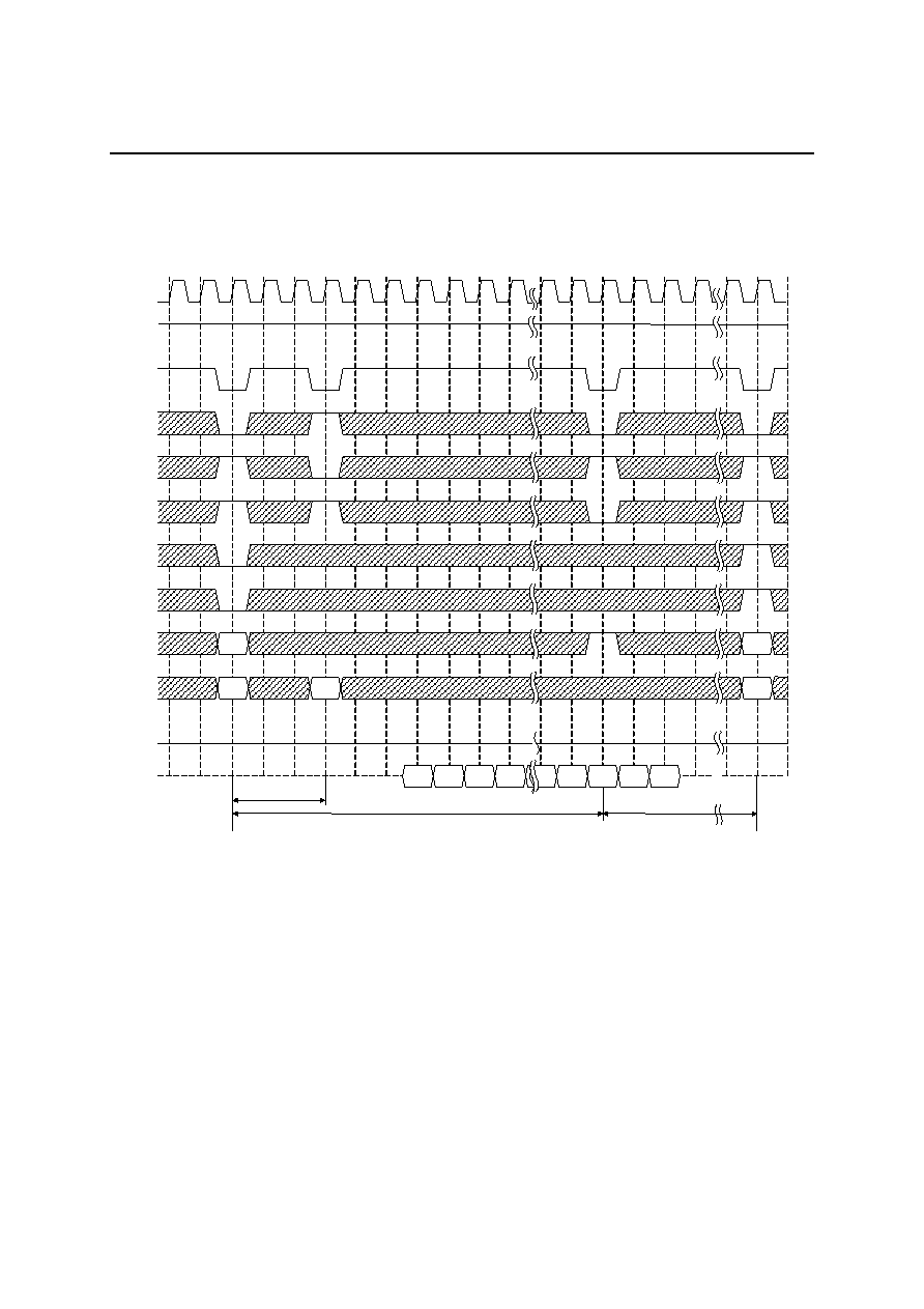
FEDS82V48540-01
OKI Semiconductor
MS82V48540
38/44
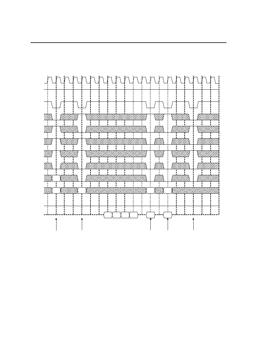
Random Column Read (Continuous Read of Same Bank) (BL = 4, CL = 3)
ACT-A
RAa
RAa
CAa
QAa1
QAa3
H
RD-A
QAa2
QAb1
QAa4
CAb
QAb2
QAc2
QAc1
RAi
RAi
PRE-A
ACT-A
L
RD-A RD-A
CAc
QAc4
QAc3
0 1 2 3 4 5 6 7 8 9 10
11 12
13 14
15 16 17 18 19
CLK
CKE
CS
CAS
WE
BA0
ADD
A10
/AP
DQM
0 - 3
DQ
RAS
BA1
FEDS82V48540-01
OKI Semiconductor
MS82V48540
39/44
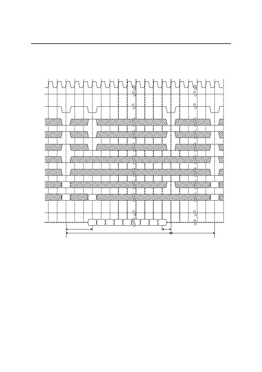
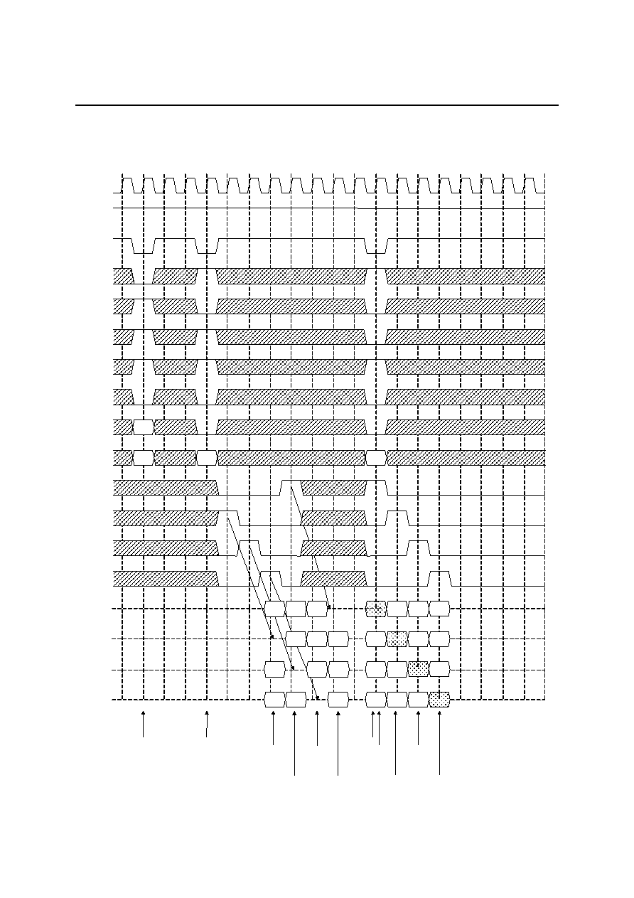
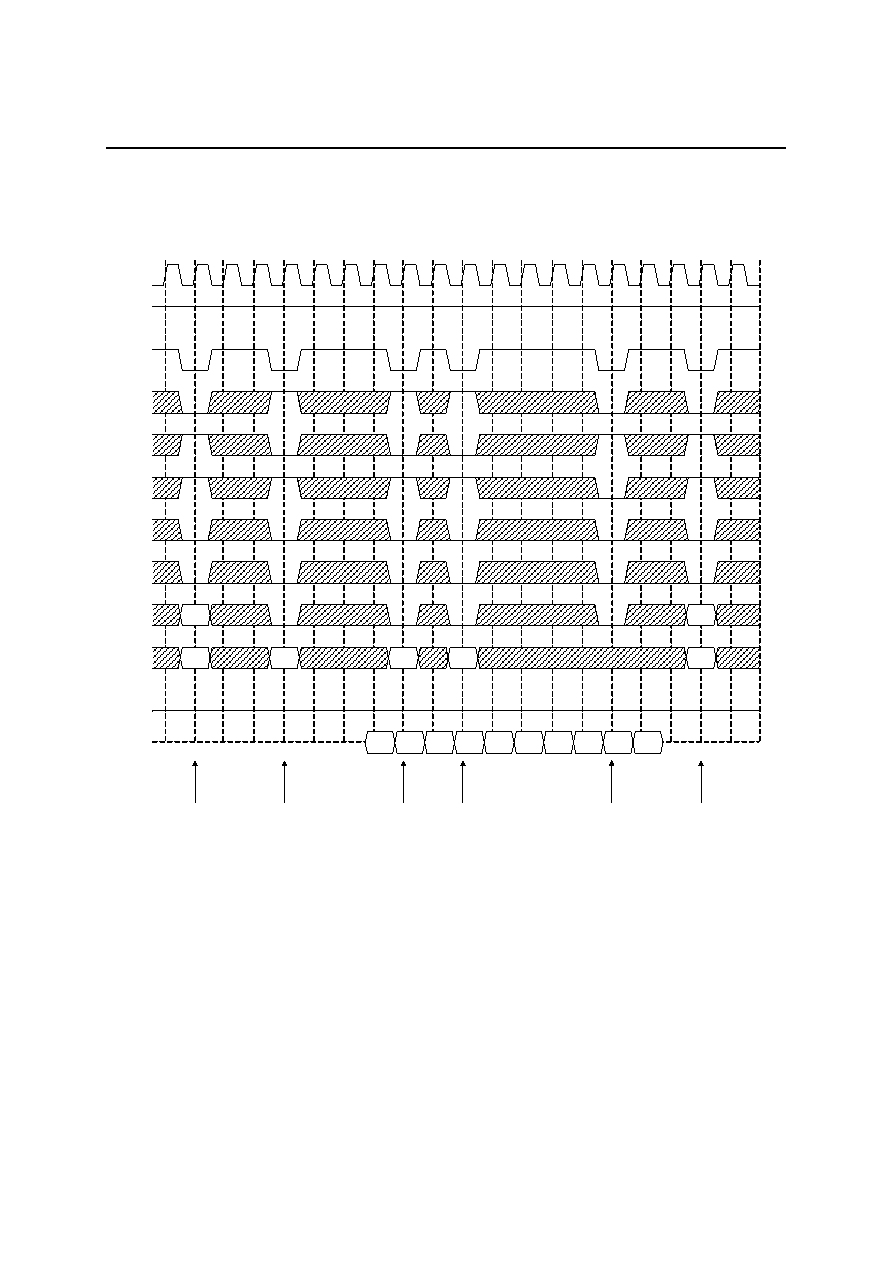
Random Column Write (Continuous Write of Same Bank) (BL = 4, CL = 3)
ACT-B
RBa
RBa
CBa
DBa1
DBa3
H
WT-B
DBa2
DBb1
DBa4
CBb
CBc
DBb2
DBc2
DBc1
RBi
RBi
PRE-B
ACT-B
L
DBc4
DBc3
WT-B WT-B
0 1 2 3 4 5 6 7 8 9 10
11 12 13 14 15 16 17 18 19
CLK
CKE
CS
CAS
WE
BA0
ADD
A10
/AP
DQM
0 - 3
DQ
RAS
BA1
FEDS82V48540-01
OKI Semiconductor
MS82V48540
40/44
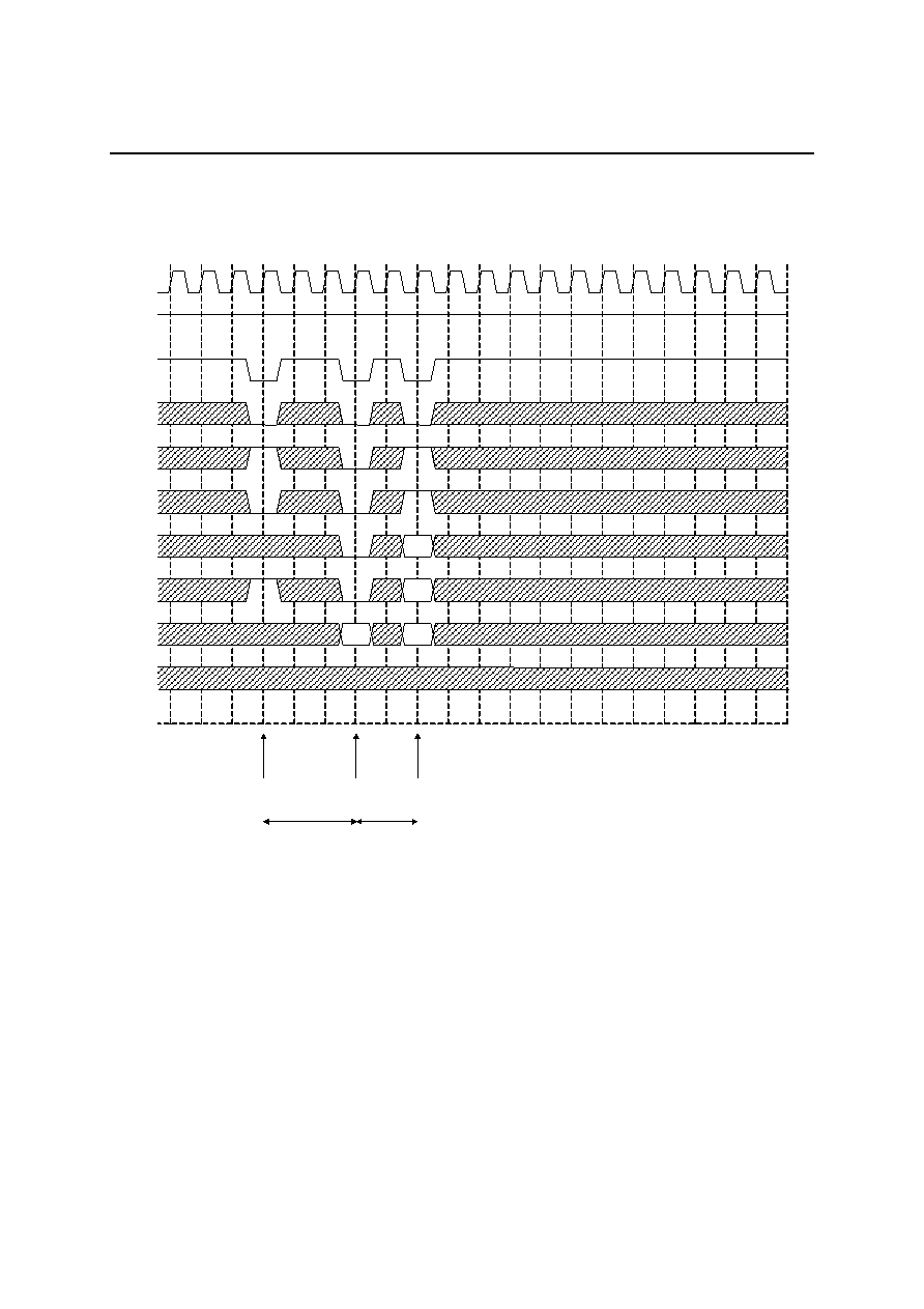
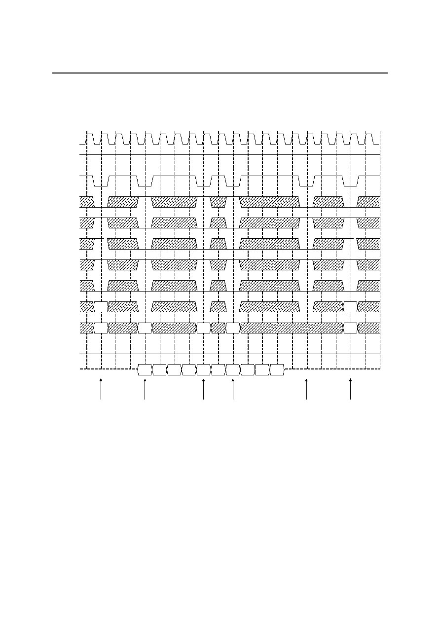
Interleaved Column Read (BL = 4, CL = 3)
ACT-A
RAa
RAa
CAa
CBa
CBb
QAa1
QAa3
H
RD-A
QAa2
QBa1
QAa4
CAb
QBa2
QBc2
QBb1
PRE-B
PRE-A
RBa
RBa
QAb2
QAb1
ACT-B
RD-B
t
RCD
t
RRD
L
QAb4
QAb3
RD-A
RD-B
0 1 2 3 4 5 6 7 8 9 10
11 12 13 14 15 16 17 18 19
CLK
CKE
CS
CAS
WE
BA0
ADD
A10
/AP
DQM
0 - 3
DQ
RAS
BA1

FEDS82V48540-01
OKI Semiconductor
MS82V48540
41/44
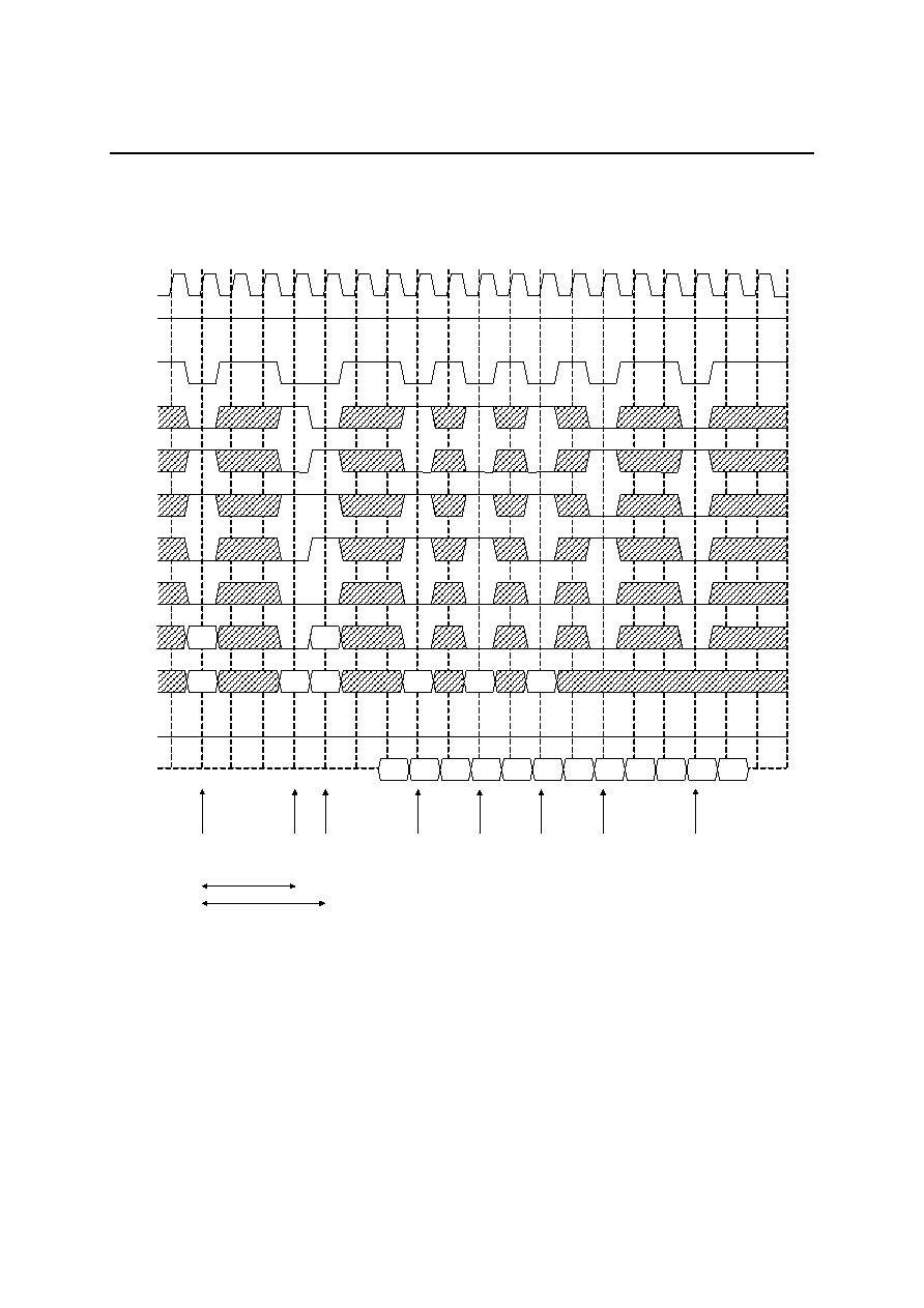
Interleaved Column Write (BL = 4, CL = 3)
ACT-C
RCa
RCa
DCa1
DCa3
H
WT-C
DCa2
DDa1
DCa4
DDa2
DDb2
DDb1
PRE-D
PRE-C
DCb2
DCb1
ACT-D
WT-D
WT-C
t
RCD
t
RRD
L
CCa
CDa
CDb
CCb
RDa
RDa
WT-D
DCb4
DCb3
0 1 2 3 4 5 6 7 8 9 10 11 12 13 14 15 16 17 18 19
CLK
CKE
CS
CAS
WE
BA0
ADD
A10
/AP
DQM
0 - 3
DQ
RAS
BA1
FEDS82V48540-01
OKI Semiconductor
MS82V48540
42/44
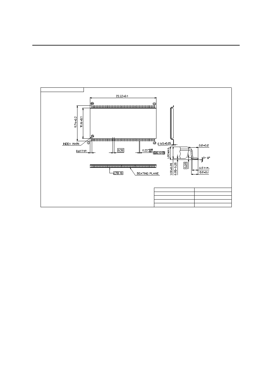
PACKAGE DIMENSIONS
TSOP(2)86-P-400-0.50-K
Mirror finish
Package material
Epoxy resin
Lead frame material
42 alloy
Pin treatment
Solder plating (
5�m)
Package weight (g)
0.53 TYP.
5
Rev. No./Last Revised
1/Jul. 14, 1998
Notes for Mounting the Surface Mount Type Package
The surface mount type packages are very susceptible to heat in reflow mounting and humidity
absorbed in storage.
Therefore, before you perform reflow mounting, contact Oki's responsible sales person for the product
name, package name, pin number, package code and desired mounting conditions (reflow method,
temperature and times).
(Unit: mm)
FEDS82V48540-01
OKI Semiconductor
MS82V48540
43/44
REVISION HISTORY
Page
Document
No.
Date
Previous
Edition
Current
Edition
Description
� �
First
edition
Changed the speed rank indication in
"Package" of the FEATURES Section
from "XX to "x".
1 1
Changed the device names in the Family
column in the table of the PRODUCT
FAMILY Section.
22 22
Changed the names of the family
devices in the table of the DC
Characteristics Section.
24 24
Changed the names of the family
devices in the table of the Synchronous
Characteristics Section.
FEDS82V48540-01
Nov. 8, 2002
25 25
Changed the names of the family
devices in the table of the Asynchronous
Characteristics Section.

FEDS82V48540-01
OKI Semiconductor
MS82V48540
44/44
NOTICE
1. The information contained herein can change without notice owing to product and/or technical improvements.
Before using the product, please make sure that the information being referred to is up-to-date.
2. The outline of action and examples for application circuits described herein have been chosen as an
explanation for the standard action and performance of the product. When planning to use the product, please
ensure that the external conditions are reflected in the actual circuit, assembly, and program designs.
3. When designing your product, please use our product below the specified maximum ratings and within the
specified operating ranges including, but not limited to, operating voltage, power dissipation, and operating
temperature.
4. Oki assumes no responsibility or liability whatsoever for any failure or unusual or unexpected operation
resulting from misuse, neglect, improper installation, repair, alteration or accident, improper handling, or
unusual physical or electrical stress including, but not limited to, exposure to parameters beyond the specified
maximum ratings or operation outside the specified operating range.
5. Neither indemnity against nor license of a third party's industrial and intellectual property right, etc. is
granted by us in connection with the use of the product and/or the information and drawings contained herein.
No responsibility is assumed by us for any infringement of a third party's right which may result from the use
thereof.
6. The products listed in this document are intended for use in general electronics equipment for commercial
applications (e.g., office automation, communication equipment, measurement equipment, consumer
electronics, etc.). These products are not authorized for use in any system or application that requires special
or enhanced quality and reliability characteristics nor in any system or application where the failure of such
system or application may result in the loss or damage of property, or death or injury to humans.
Such applications include, but are not limited to, traffic and automotive equipment, safety devices, aerospace
equipment, nuclear power control, medical equipment, and life-support systems.
7. Certain products in this document may need government approval before they can be exported to particular
countries. The purchaser assumes the responsibility of determining the legality of export of these products
and will take appropriate and necessary steps at their own expense for these.
8.
No part of the contents contained herein may be reprinted or reproduced without our prior permission.
Copyright 2002 Oki Electric Industry Co., Ltd.