 | –≠–ª–µ–∫—Ç—Ä–æ–Ω–Ω—ã–π –∫–æ–º–ø–æ–Ω–µ–Ω—Ç: KGL4115F | –°–∫–∞—á–∞—Ç—å:  PDF PDF  ZIP ZIP |

1Electronic Components
June 28, 2002
GTD-18111 Rev. 8.0
KGL4115F
10 Gbps EA Modulator Driver IC
1/6
FEATURES
∑ High Output Voltage: Maximum Amplitude > 2.7 Vpp
∑ X-Point Control Function
∑ Output Amplitude Control Function
∑ Output Bias Control Function
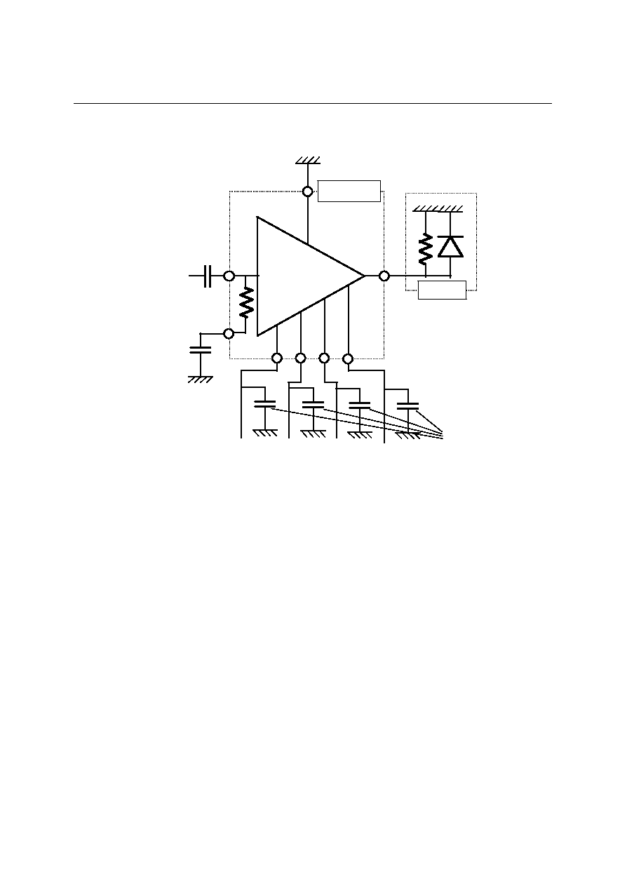
FUNCTION DIAGRAM
ABSOLUTE MAXIMUM RATINGS
Parameter
Symbol
Min
Max
Unit
Note
Supply Voltage
VS
-6.5
0.3
V
X-Point Control Voltage
VB1
VS-4.8
(Min. -6.5)
VS+2.4
(Max. 0.3)
V
Output Amplitude Control Voltage
VC1
-6.5
VS+1.2
(Max. 0.3)
V
Output Bias Control Voltage
VC2
-6.5
VS+2.4
(Max. 0.3)
V
Operating Temperature at Package
Base
Ts
-10
100
∞C
Storage Temperature
Tst
-40
125
∞C
RECOMMENDED OPERATING CONDITIONS
Parameter
Symbol
Min
Typ
Max
Unit
Supply Voltage
VS
-5.5
-5.0
V
X-Point Control Voltage
VB1
VS+0.8
VS+2.2
V
Output Amplitude Control Voltage
VC1
VS
VS+1.0
V
Output Bias Control Voltage
VC2
VS
VS+2.2
V
Operating Temperature at Package Base
Ts
0
70
∞C
Input Interface
AC coupled (External blocking capacitor is required)
Output Interface
DC coupled
OUT
IN
VB1 VB2
VS
VC1 VC2
GTD-18111 Rev.8.0
1Electronic Components
KGL4115F
2/6
ELECTRICAL CHARACTERISTICS
Parameter
Symbol
Condition
Min
Typ
Max
Unit
Supply Current
Iss
including bias
current = 20 mA
285
mA
Voltage Offset
Vo (ofs)
50
load, bias
current = 20 mA
-1
0
V
Input Amplitude
Vin
0.5
1
Vpp
Output Amplitude (Max)
Vo (Max)
50
load
2.7
Vpp
Output Low Voltage (Min)
V (LO)
50
load
-3
V
Output High Voltage (Min)
V (HI)
50
load
-1
V
X-Point Control
Xp
NRZ, 50
load
20
80
%
X-Point Stability
Del (Xp)
0≠70∞C
50
load
10
%
Output Rise/Fall Time
Tr/Tf
50
load
20%/80%
40
ps
Input Return Loss
S11
100 kHz≠10 GHz
15
dB
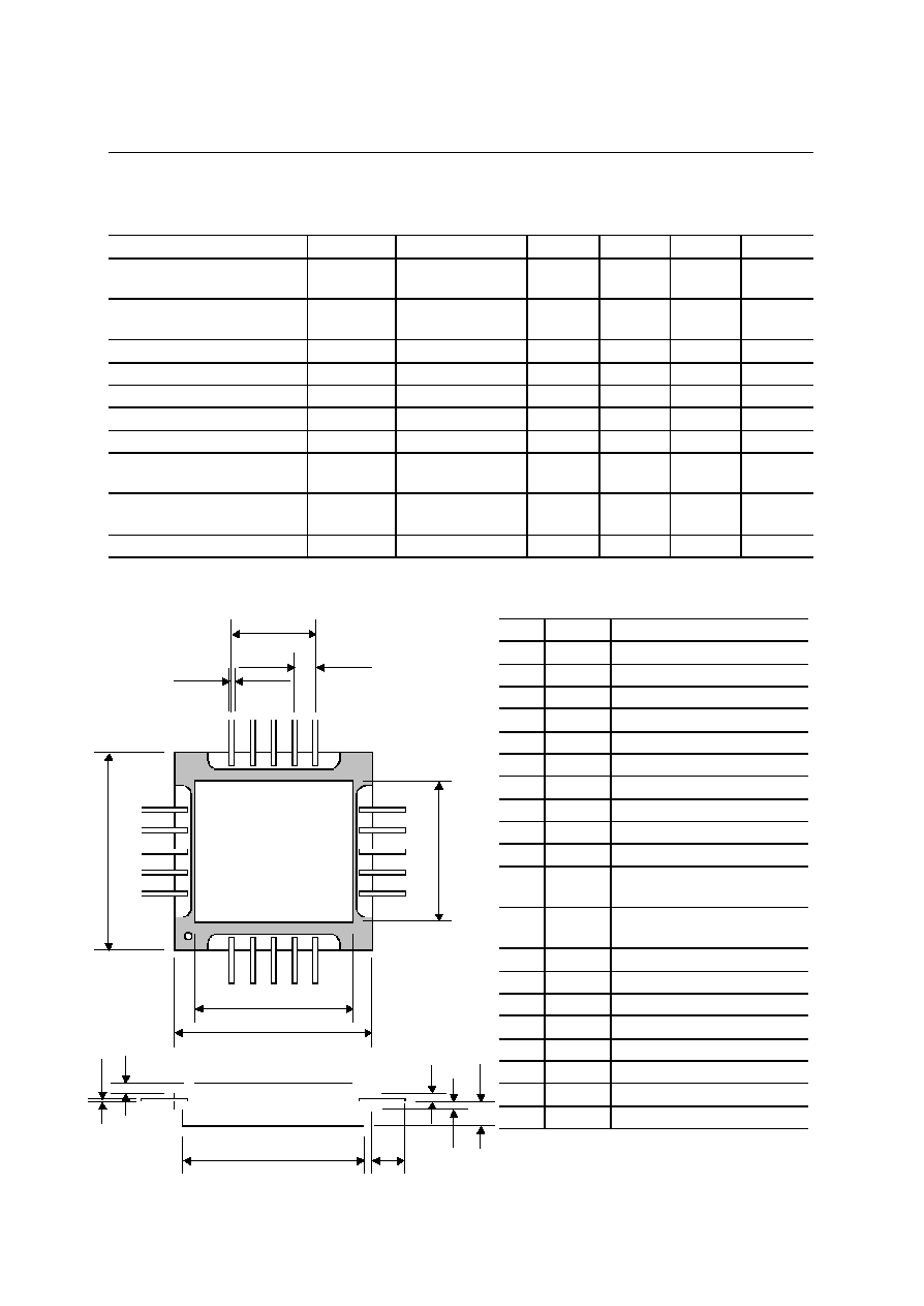
PACKAGE DIMENSIONS
PINCONNECTION
No. Symbol
Note
1
N.C.
No Connection
2
N.C.
No Connection
3
N.C.
No Connection
4
N.C.
No Connection
5
N.C.
No Connection
6
GND
Ground
7
OUT
Signal Output Port
8
GND
Ground
9
N.C.
No Connection
10
GND
Ground
11
VC2
Output Bias Control Voltage
Port
12
VC1
Output Amplitude Control
Voltage Port
13
VS
Supply Voltage Port
14
VB2
Input Termination Port
15
VB1
X-Point Control Voltage Port
16
GND
Ground
17
N.C.
No Connection
18
GND
Ground
19
IN
Signal Input Terminal
20
GND
Ground
(Top View)
(Unit : mm)
9.6
12±0.2
20-0.3
5.08
16-1.27
1
5
6
10
11
15
16
20
KGL4115F
1
JAPAN
XXX
12±0.2
8.6
11
2±0.3
0.
125
0.5
0.6
0.5
1.5
GTD-18111 Rev.8.0
1Electronic Components
KGL4115F
3/6
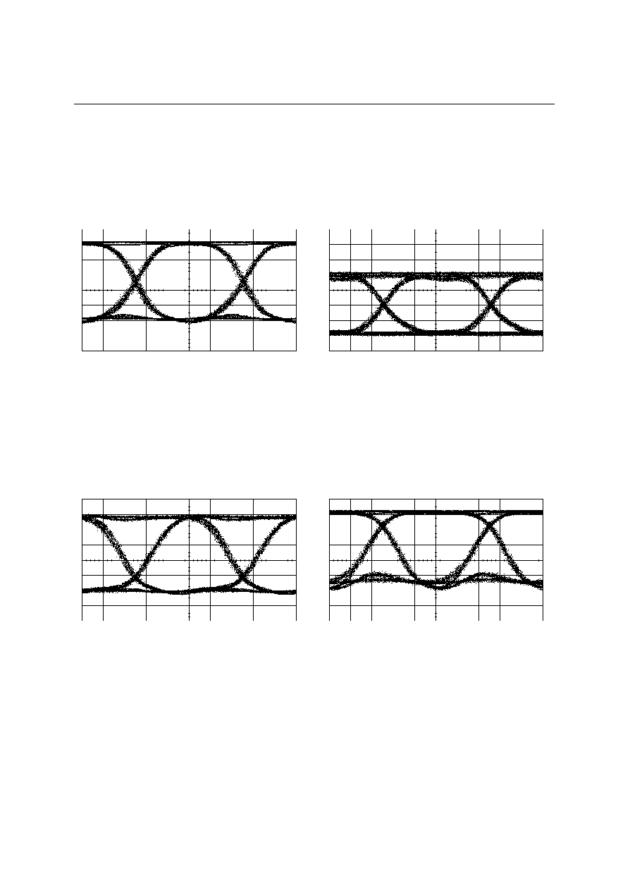
TYPICAL CHARACTERISTICS ( WAVEFORM )
Measured Condition
Display Factor V : 600 mV/div, H : 20 ps/div, Offset : -2.2V
Input Signal 10 Gbps, PN31, PRBS, 0.5 Vpp, Tr/Tf = 40 ps/38.2 ps (20≠80%)
Waveform @ Cross Point
50% Waveform @ Maximum Offset
Waveform @ Cross Point
20% Waveform @ Cross Point
80%
Note
Jitter(p-p) means " 6
◊
Jitter(RMS) ".
Operating Condition
VB1 = ≠3.797 V (@Xp=50.0%)
VC1 = ≠4.525 V
VC2 = ≠5.0 V (Output Offset : Off)
VS = ≠5.0 V (IS = 192.2 mA)
Output Amplitude
: 2.956 Vpp
Rise Time (20≠ 80%)
: 28.4 ps
Fall Time (20≠ 80%)
: 24.9 ps
Jitter (p -p)
: 10.4 ps
Operating Condition
VB1 = ≠3.660 V (@Xp=19.5%)
VC1 = ≠4.525 V
VC2 = ≠5.0 V (Output Offset : Off)
VS = ≠5.0 V (IS = 192.2 mA)
Output Amplitude
: 2.868 Vpp
Rise Time (20≠ 80%)
: 28.4 ps
Fall Time (20≠ 80%)
: 26.7 ps
Jitter (p -p)
: 11.1 ps
Operating Condition
VB1 = ≠3.945 V (@Xp=80.5%)
VC1 = ≠4.525 V
VC2 = ≠5.0 V (Output Offset : Off)
VS = ≠5.0 V (IS = 191.9 mA)
Output Amplitude
: 2.724 Vpp
Rise Time (20≠ 80%)
: 25.8 ps
Fall Time (20≠ 80%)
: 24.4 ps
Jitter (p -p)
: 9.9 ps
Operating Condition
VB1 = ≠3.810 V (@Xp=49.8%)
VC1 = ≠4.525 V
VC2 = ≠2.8 V (Output Offset : Max)
VS = ≠5.0 V (IS = 244.9 mA)
Output Offset
: 1.260 V
Rise Time (20≠ 80%)
: 25.8 ps
Fall Time (20≠ 80%)
: 28.0 ps
Jitter (p -p)
: 9.7 ps
GTD-18111 Rev.8.0
1Electronic Components
KGL4115F
4/6
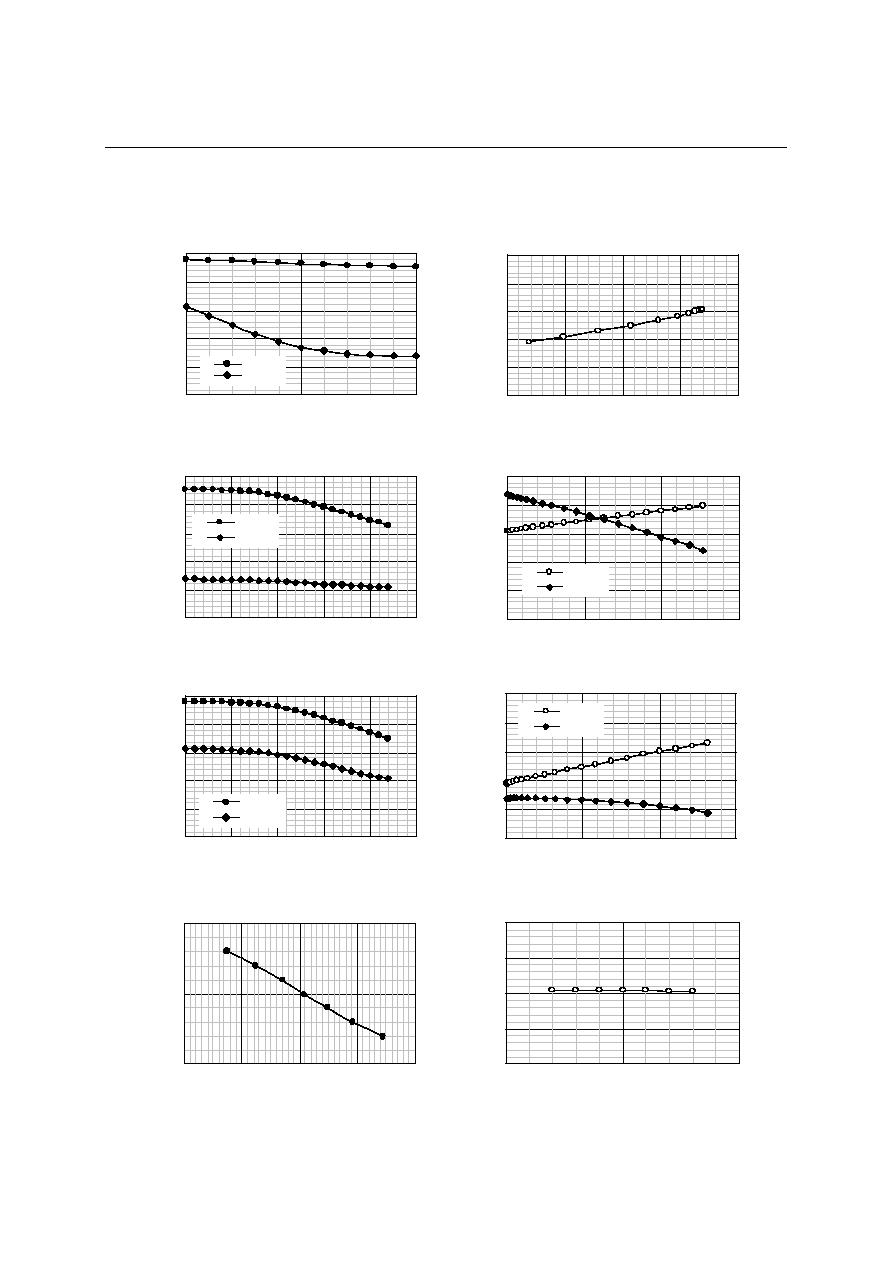
TYPICAL CHARACTERISTICS ( CONTROL BIAS DEPENDENCE )
Note Input Signal : 10 Gbps, PN31, PRBS, 0.5 Vpp, Tr/Tf = 40 ps/38.2 ps (20≠80%)
-5.0
-4.0
-3.0
-2.0
-1.0
0.0
-5.0
-4.5
-4.0
-3.5
-3.0
-2.5
VC2 [V]
Output Voltage [V]
Vhigh
Vlow
Dependence of Output Voltage on VC2
@Vs=-5V,VC1=-4V,Xp:50%
100
150
200
250
300
0
50
100
Cross point [%]
Supply Current [mA]
Cross Point Dependence
@Vs=-5V,VC2=-4V
-5.0
-4.0
-3.0
-2.0
-1.0
0.0
-5.0
-4.5
-4.0
VC1 [V]
Output Voltage [V]
Vhigh
Vlow
Dependence of Output Voltage on VC1
@Vs=-5V,VC2=-5V,Xp:50%
-5.0
-4.0
-3.0
-2.0
-1.0
0.0
-5.0
-4.5
-4.0
-3.5
-3.0
-2.5
VC2 [V]
Output Voltage [V]
Vhigh
Vlow
Dependence of Output Voltage on VC2
@Vs=-5V,VC1=-5V,Xp:50%
50
100
150
200
250
300
1.5
2.0
2.5
3.0
3.5
Output Amplitude [Vpp]
Supply Current [mA]
Output Amplitude Dependence
@Vs=-5V,VC2=-5V,Xp:50%
0
50
100
-4.0
-3.9
-3.8
-3.7
-3.6
VB1 [V]
Output Cross Point [%]
Dependence of Output Cross Point on VB1
@Vs=-5V,VC2=-5V
50
100
150
200
250
300
0.0
0.5
1.0
1.5
Offset Voltage [V]
Supply Current [mA]
1
1.5
2
2.5
3
3.5
Is
Vamp
Offset Voltage Dependence
@Vs=-5V,VC1=-5V,Xp:50%
Output Amplitude [Vpp]
50
100
150
200
250
300
0.0
0.5
1.0
1.5
Offset Voltage [V]
Supply Current [mA]
1
1.5
2
2.5
3
3.5
Is
Vamp
Offset Voltage Dependence
@Vs=-5V,VC1=-4V,Xp:50%
Output Amplitude [Vpp]
GTD-18111 Rev.8.0
1Electronic Components
KGL4115F
5/6
TYPICAL APPLICATION
APPLICATION NOTE
1. For stable operation;
1-1. To prevent a dependence of "X-Point" on the supply voltage VS,
(1) Use an external voltage source of ≠3.8V for "VB2", or
(2) Control the voltage of "VB1", so that the voltage difference "VB1≠ VB2" is constant.
1-2. To prevent a dependence of "Output amplitude" on the supply voltage VS,
Control the voltage of "VC1", so that the voltage difference "VC1≠ VS" is constant.
1-3. To prevent a dependence of "Output bias control voltage" on supply voltage VS,
Control the voltage of "VC2", so that the voltage difference "VC2≠ VS" is constant.
2. Power-up/shut-down sequence;
For power-up, supply control voltages (VB1, (VB2), VC1, VC2) at first, then Vs. For shut-down,
Vs at first, then control voltages.
Customer does not need to care about the sequence for the control voltages (VB1,(VB2),VC1,VC2).
Output Bias
Control
Data Input
IN
VB1 VS
VC1 VC2
OUT
GND
Blocking
Capacitor
Ex. 0.1
µ
F
Chip
Capacitor
0.1
µ
F
Supply Voltage
Output
Amplitude
X
-
Point Control
VB2
KGL4115F
EAM
50
Chip
Capacitor
0.1
µ
F

GTD-18111 Rev.8.0
1Electronic Components
KGL4115F
6/6
SAFETY AND HANDRING INFORMATION ON GaAs DEVICES
Arsenic Compound (GaAs Devices)
The product contains arsenic (As) as a compound.
This material is stable for normal use, however, its dust or vapor may be potentially hazardous to the human
body.
Avoid ingestion, fracture, burning or chemical treatment to the product.
∑ Do not put the product in your mouth.
∑ Do not burn or destroy the product.
∑ Do not perform chemical treatment for the product.
Keep laws and ordinances related to the disposal of the products.
NOTICE
1. The information contained herein can change without notice owing to product and/or technical improvements.
Before using the product, please make sure that the information being referred to is up-to-date.
2.
The outline of action and examples for application circuits described herein have been chosen as an
explanation for the standard action and performance of the product. When planning to use the product, please
ensure that the external conditions are reflected in the actual circuit, assembly, and program designs.
3.
When designing your product, please use our product below the specified maximum ratings and within the
specified operating ranges including, but not limited to, operating voltage, power dissipation, and operating
temperature.
4.
Oki assumes no responsibility or liability whatsoever for any failure or unusual or unexpected operation
resulting from misuse, neglect, improper installation, repair, alteration or accident, improper handling, or
unusual physical or electrical stress including, but not limited to, exposure to parameters beyond the specified
maximum ratings or operation outside the specified operating range.
5.
Neither indemnity against nor license of a third party's industrial and intellectual property right, etc. is
granted by us in connection with the use of the product and/or the information and drawings contained herein.
No responsibility is assumed by us for any infringement of a third party's right which may result from the use
thereof.
6.
The products listed in this document are intended for use in general electronics equipment for commercial
applications (e.g., office automation, communication equipment, measurement equipment, consumer
electronics, etc.). These products are not authorized for use in any system or application that requires special
or enhanced quality and reliability characteristics nor in any system or application where the failure of such
system or application may result in the loss or damage of property, or death or injury to humans.
Such applications include, but are not limited to, traffic and automotive equipment, safety devices, aerospace
equipment, nuclear power control, medical equipment, and life-support systems.
7.
Certain products in this document may need government approval before they can be exported to particular
countries. The purchaser assumes the responsibility of determining the legality of export of these products
and will take appropriate and necessary steps at their own expense for these.
8.
No part of the contents contained herein may be reprinted or reproduced without our prior permission.
Copyright 2002 Oki Electric Industry Co., Ltd.