 | –≠–ª–µ–∫—Ç—Ä–æ–Ω–Ω—ã–π –∫–æ–º–ø–æ–Ω–µ–Ω—Ç: KGL4217L | –°–∫–∞—á–∞—Ç—å:  PDF PDF  ZIP ZIP |

GTD-18289 Rev. 3.0
Electronic Components
Nov.
2001
KGL4217L
Preliminary
Limiting Amplifier IC
DESCRIPTION
KGL4217L, limiting Amplifier IC with 0.18
µm gate length GaAs MESFETs, has been designed for 10 Gb/s
digital communication systems. By using DCFL(Direct Coupled FET Logic), high speed operation of 10 Gb/s
and low power dissipation have been realized. Capacitive coupling is recommended for I/O connections.
FUNCTION DIAGRAM
ABSOLUTE MAXIMUM RATINGS
Items
Symbol
Min.
Max.
Units
Supply Voltage
V
DD
--0.3
2.3
V
Applied Voltage at DIN, DR1
VDI
--0.3
1.5
V
Applied Voltage at DR2
VRI
--2.5
2.5
V
Temperature at Package Base under Bias
Ts
--45
100
°C
Storage Temperature
Tst
--45
125
°C
ELECTRICAL CHARACTERISTICS
V
DD
= 2 V
± 0.1 V, Ts = 0 to 70∞C
Items
Symbol
Min.
Typ.
Max.
Units
Maximum Operating Data Bit Rate
DAR
10
Gb/s
Power Dissipation
PW
0.25
0.35
W
Data Input Voltage Swing
VI
0.035
0.6
Vpp
Data Output Voltage Swing
VO
0.4
0.6
0.9
Vpp
DIN:
Data Input
DR1:
RF Bypass for Data Threshold Level Stability
DR2:
Data Threshold Control (Duty Cycle Control )
Q, QN: Complimentary Data Outputs
V
DD
:
Power Supply
50
DR1
V
DD
V
DD
5
Q
QN
DIN
DR2
V
DD
GTD-18289
1
Electronic Components
KGL4217L
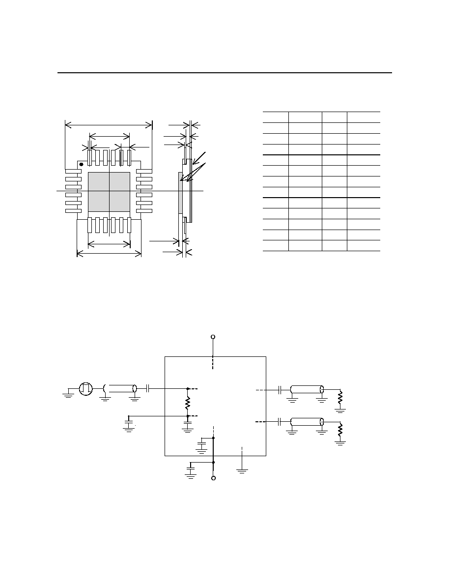
PACKAGE DIMENSIONS
PIN ASSIGNMENT
No.
Symbol
No.
Symbol
1
GND
13
GND
2
QN
14
GND
3
GND
15
GND
4
GND
16
GND
5
Q
17
DIN
6
GND
18
GND
7
GND
19
V
DD
8
DR2
20
GND
9
GND
21
GND
10
DR1
22
GND
11
DR1
23
V
DD
12
DR1
24
GND
INTERFACE CONFIGURATION
(Top View)
7
13
19
1
6.35
0.30
13.8
± 0.3
1.27
7.4 SQ
9.61 SQ
0.125
0.20
0.50
0.50
0.64
± 0.2
Ceramic
CuW
Unit: mm
NOTE
- Capacitive coupling is recommended for high speed I/O terminals (DIN, Q, QN).
- DR1 is RF bypass terminal for data threshold level stability and should be connected to
ground through a RF bypass capacitor (0.1
µF). The data threshold level is fixed by
the internal self-bias cirsuit, or by the voltage applied from an external supply.
- DR2 is a data threshold control terminal, or is connected to ground through a capacitor
QN 2
VDD
0.1uF
19,23
2.0V
KGL4217L
IC boundary
DR2
8
GND
1, 3, 4, 6, 7, 9, 13, 14, 15,
16, 18, 20, 21, 22, 24
17 DIN
50
10,11,12 DR1
Internal Bias
Q 5
Zo=50
Zo=50
0.1uF
50
50

GTD-18289
1
Electronic Components
KGL4217L
TYPICAL CHARACTERISTICS
Measurement condition : PRBS 2
31
-1, BER=10
-9
Measurement condition : DAR=10Gb/s,
PRBS 2
31
-1, VDD=2V, PW=250mW
VI=10 mVp-p
VI=35 mVp-p
VI=600 mVp-p
Vert.: 120 mV/div, Horiz.: 25 ps/div
Output Waveforms
1 10 100 1000
Input Voltage Swing ( mVp-p )
0
100
200
300
400
500
600
700
Output V
oltage Swing
(
mVp-p )
Output Voltage Swing vs. Input Voltage Swing
2
4
6
8
10
12
14
0
2
4
6
8
10
12
14
VDD=1.8V
VDD=2.0V
VDD=2.2V
Minimum Input V
oltage Swing [
mVp-p]
Input Data Bit Rate [Gb/s]
Measurement condition : PRBS 2
31
-1, BER=10
-9
Sensitivity vs. Data Bit Rate

GTD-18289
1
Electronic Components
KGL4217L
Duty Cycle vs. Data Threshold Control
0 0.2 0.4 0.6 0.8 1.0
40
45
50
55
60
Data Threshold Control Voltage V
DR2
[V]
Duty Cycle [%]
Input Voltage Swing
35 mVp-p
600 mVp-p
Input Stage of KGL4217L
DIN
DR1
IC Boundary
Sign Wave
DR2
V
DR2