LM91
Diode Input Digital Temperature Sensor with Two-Wire
Interface
General Description
The
LM91
is
a
remote
diode
temperature
sensor,
Delta-Sigma
analog-to-digital
converter,
and
digital
over-temperature detector with an SMBus
TM
interface. The
LM91 senses its own temperature as well as the tempera-
ture of a target IC with a diode junction, such as a Pentium
Æ
II processor or a diode connected 2N3904. A diode junction
(semiconductor junction) is required on the target IC's die. A
host can query the LM91 at any time to read the temperature
of this diode as well as the temperature state of the LM91
itself. A T_CRIT_A interrupt output becomes active when the
temperature is greater than a programmable comparator
limit, T_CRIT.
The host can program as well as read back the state of the
T_CRIT register. Power up default values for T_CRIT are as
shown in the ordering information table. Three state logic
inputs allow two pins (ADD0, ADD1) to select up to 9 SMBus
address locations for the LM91.
Features
n
Directly senses die temperature of remote ICs
n
Senses temperature of remote diodes
n
SMBus compatible interface, supports SMBus Timeout
n
Register readback capability
n
7 bit plus sign temperature data format
n
2 address select lines enable 9 LM91s to be connected
to a single bus
Key Specifications
j
Supply Voltage
3.0V - 3.6V
j
Supply Current
1 mA (max)
j
Local Temperature Accuracy
±
1.0∞C (typ)
j
Remote Diode Temperature Accuracy
+60∞C to +100∞C
±
4∞C (max)
0∞C to +125∞C
±
6∞C (max)
Applications
n
System Thermal Management
n
Personal Computers
n
Electronic Test Equipment
n
Office Electronics
n
HVAC
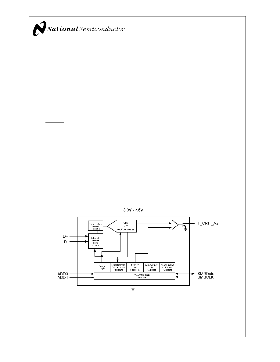
Simplified Block Diagram
20034301
# Indicates Active Low ("NOT")
SMBus
TM
is a trademark of the Intel Corporation.
Pentium
Æ
II processor is a registered trademark of the Intel Corporation.
I2C
Æ
is a registered trademark of the Philips Corporation.
November 2001
LM91
Diode
Input
Digital
T
emperature
Sensor
with
T
wo-W
ire
Interface
© 2001 National Semiconductor Corporation
DS200343
www.national.com
Connection Diagram
QSOP-16
20034302
TOP VIEW
Ordering Information
Order Number
NS Package
Number
Transport
Media
SMBus
Revision
Level
Noise Filter
on SMBCLK
Remote Diode
Accuracy
Local
T_CRIT
Default
Remote
T_CRIT
Default
LM91DIMQA
MQA16A
(QSOP-16)
95 Units in
Rail
1.1
20MHz
±
4∞C
127∞C
95∞C
LM91DIMQAX
MQA16A
(QSOP-16)
2500 Units on
Tape and Reel
1.1
20MHz
±
4∞C
127∞C
95∞C
LM91
www.national.com
2
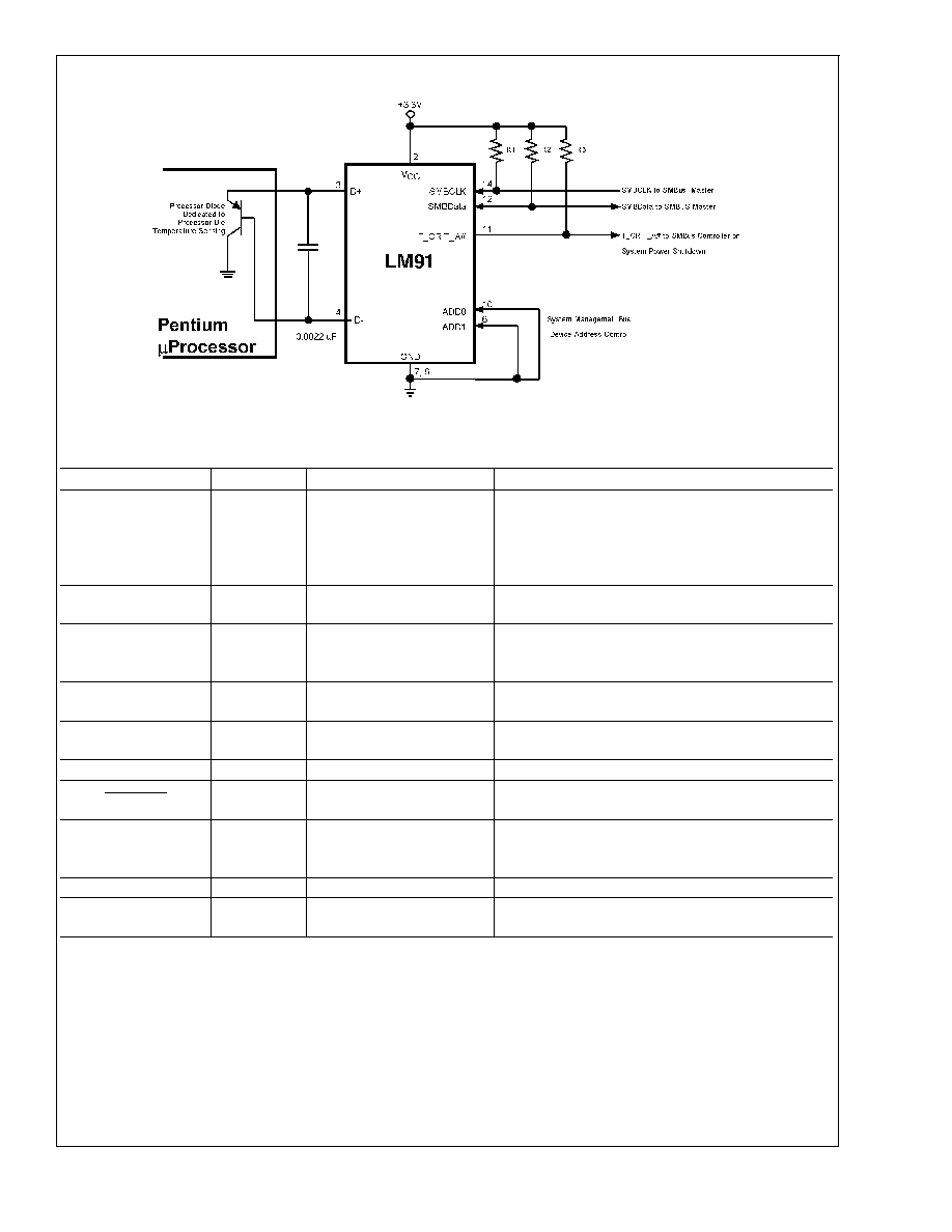
Typical Application
20034303
Pin Descriptions
Label
Pin #
Function
Typical Connection
NC
1, 5, 9, 13,
16
Manufacturing test pins.
Left floating. PC board traces may be routed
through the pads for these pins. Although, the
components that drive these traces should share the
same supply as the LM91 so that the Absolute
Maximum Voltage at any Pin rating is not violated.
V
CC
2
Positive Supply Voltage
Input
DC Voltage from 3.0V to 3.6V
D+
3
Diode Current Source
To Diode Anode. Connected to remote discrete
diode or to the diode on the external IC whose die
temperature is being sensed.
D-
4
Diode Return Current Sink
To Diode Cathode. Must be grounded when not
used.
ADD0≠ADD1
10, 6
User-Set SMBus (I
2
C)
Address Inputs
Ground (Low, "0"), V
CC
(High, "1") or open
("TRI-LEVEL")
GND
7, 8
Power Supply Ground
Ground
T_CRIT_A
11
Critical Temperature
Alarm, open-drain output
Pull Up Resistor, Controller Interrupt Line or System
Shutdown
SMBData
12
SMBus (I
2
C) Serial
Bi-Directional Data Line,
open-drain output
From and to Controller, Pull Up Resistor
SMBCLK
14
SMBus (I
2
C) Clock Input
From Controller
NC
15
No Connection
Left floating. PC board traces may be routed
through the pads for this pin.
LM91
www.national.com
3
Absolute Maximum Ratings
(Note 1)
Supply Voltage
-0.3V to 6.0V
Voltage at Any Pin:
NC (Pins 1,5,9), ADD0, ADD1, D
+
-0.3V to
(V
CC
+ 0.3V)
All other pins (except D-)
-0.3V to 6.0V
D- Input Current
±
1 mA
Input Current at All Other Pins (Note
2)
5 mA
Package Input Current (Note 2)
20 mA
SMBData, T_CRIT_A Output Sink
Current
10 mA
Output Voltage
6.0V
Storage Temperature
-65∞C to +150∞C
Soldering Information, Lead Temperature
QSOP Package (Note 3)
Vapor Phase (60 seconds)
215∞C
Infrared (15 seconds)
220∞C
ESD Susceptibility (Note 4)
Human Body Model
2500V
Machine Model
250V
Operating Ratings
(Note 1) and (Note 5)
Specified Temperature Range
T
MIN
to T
MAX
LM91D
0∞C to +125∞C
Supply Voltage Range (V
CC
)
+3.0V to +3.6V
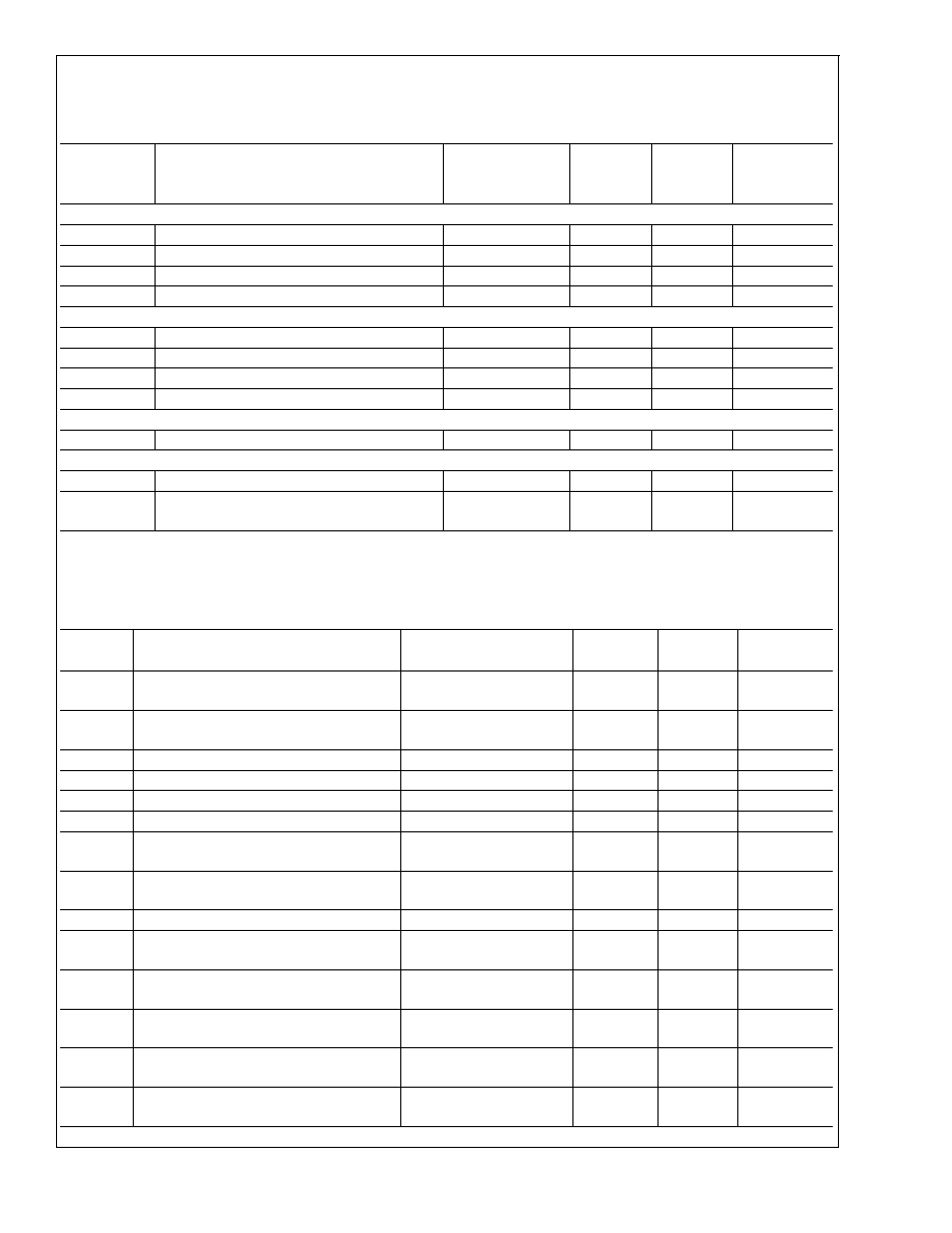
Temperature-to-Digital Converter Characteristics
Unless otherwise noted, these specifications apply for V
CC
=+3.0 Vdc to +3.6 Vdc. Boldface limits apply for T
A
= T
J
= T
MIN
to T
MAX
; all other limits T
A
= T
J
=+25∞C, unless otherwise noted.
Parameter
Conditions
Typical
LM91D
Limits
Units
(Note 6)
(Note 7)
(Limit)
Local Temperature Error (Note 8)
±
1
∞C
Remote Temperature Error using Pentium Diode
(Note 8) and (Note 9)
+60∞C
T
A
+100∞C,
V
CC
= 3.3 Vdc
±
4
∞C (max)
0∞C
T
A
+125∞C,
V
CC
= 3.3 Vdc
±
6
∞C (max)
Remote Temperature Error using Diode
Connected 2N3904 (Note 8) and (Note 9)
+60∞C
T
A
+100∞C,
V
CC
= 3.3 Vdc
+2, -6
∞C (max)
0∞C
T
A
+125∞C,
V
CC
= 3.3 Vdc
+4, -8
∞C (max)
Resolution
8
Bits
1
∞C
Temperature Conversion Time
(Note 11)
120
145
ms
Quiescent Current (Note 10)
SMBus (I
2
C Inactive)
0.500
1
mA (max)
D- Source Voltage
0.7
V
Diode Source Current
(D+ - D-)=+ 0.65V; high
level
160
µA (max)
50
µA (min)
Low level
16
µA (max)
5
µA (min)
T_CRIT_A Output Saturation Voltage
I
OUT
= 3.0 mA
0.4
V (max)
Power-On Reset Threshold
On V
CC
input, falling edge
2.2
1.2
V (max)
V (min)
LM91
www.national.com
4
Logic Electrical Characteristics
DIGITAL DC CHARACTERISTICS
Unless otherwise noted, these specifications apply for V
CC
=+3.0 to 3.6 Vdc. Boldface limits apply for T
A
= T
J
= T
MIN
to
T
MAX
; all other limits T
A
= T
J
=+25∞C, unless otherwise noted.
Symbol
Parameter
Conditions
Typical
LM91D
Units
(Note 6)
Limits
(Note 7)
(Limit)
SMBData, SMBCLK
V
IN(1)
Logical "1" Input Voltage
2.1
V (min)
V
IN(0)
Logical "0"Input Voltage
0.8
V (max)
I
IN(1)
Logical "1" Input Current
V
IN
= V
CC
0.005
1.0
µA (max)
I
IN(0)
Logical "0" Input Current
V
IN
= 0V
-0.005
-1.0
µA (max)
ADD0, ADD1
V
IN(1)
Logical "1" Input Voltage
V
CC
1.6
V (min)
V
IN(0)
Logical "0"Input Voltage
GND
0.5
V (max)
I
IN(1)
Logical "1" Input Current
V
IN
= V
CC
50
600
µA (max)
I
IN(0)
Logical "0" Input Current
V
IN
= 0V
50
600
µA (max)
ALL DIGITAL INPUTS
C
IN
Input Capacitance
20
pF
ALL DIGITAL OUTPUTS
I
OH
High Level Output Current
V
OH
= V
CC
100
µA (max)
V
OL
SMBus Low Level Output Voltage
I
OL
= 3 mA
I
OL
= 6 mA
0.4
0.6
V (max)
SMBus DIGITAL SWITCHING CHARACTERISTICS
Unless otherwise noted, these specifications apply for V
CC
=+3.0 Vdc to +3.6 Vdc, C
L
(load capacitance) on output lines = 80
pF. Boldface limits apply for T
A
= T
J
= T
MIN
to T
MAX
; all other limits T
A
= T
J
= +25∞C, unless otherwise noted.
The switching characteristics of the LM91 fully meet or exceed the published specifications of the SMBus or I
2
C bus. The fol-
lowing parameters are the timing relationships between SMBCLK and SMBData signals related to the LM91. They are not nec-
essarily the I
2
C or SMBus bus specifications.
Symbol
Parameter
Conditions
Typical
Limits
Units
(Note 6)
(Note 7)
(Limit)
f
SMB
SMBus Clock Frequency
400
10
kHz (max)
kHz (min)
t
LOW
SMBus Clock Low Time
10% to 10%
1.3
25
µs (min)
ms (max)
t
LOW
SEXT Cumulative Clock Low Extend Time
25
ms (max)
t
HIGH
SMBus Clock High Time
90% to 90%
0.6
µs (min)
t
R;SMB
SMBus Rise Time
10% to 90%
1
µs
t
F;SMB
SMBus Fall Time
90% to 10%
0.3
µs
t
OF
Output Fall Time
C
L
= 400 pF
I
O
= 3 mA
250
ns (max)
t
TIMEOUT
SMBData and SMBCLK Time Low for
Reset of Serial Interface (Note 12)
25
40
ms (min)
ms (max)
t
1
SMBCLK (Clock) Period
2.5
µs (min)
t
2
,
t
SU;DAT
Data In Setup Time to SMBCLK High
100
ns (min)
t
3
,
t
HD;DAT
Data Out Stable after SMBCLK Low
0
0.9
ns (min)
µs (max)
t
4
,
t
HD;STA
SMBData Low Setup Time to SMBCLK
Low
100
ns (min)
t
5
,
t
SU;STO
SMBData High Delay Time after SMBCLK
High (Stop Condition Setup)
100
ns (min)
t
6
,
t
SU;STA
SMBus Start-Condition Setup Time
0.6
µs (min)
LM91
www.national.com
5