 | –≠–ª–µ–∫—Ç—Ä–æ–Ω–Ω—ã–π –∫–æ–º–ø–æ–Ω–µ–Ω—Ç: LMSM6789A | –°–∫–∞—á–∞—Ç—å:  PDF PDF  ZIP ZIP |
° Semiconductor
MSM6789A/6789L
GENERAL DESCRIPTION
The MSM6789A/6789L, an improved version of MSM6788, is a solid-state recorder developed using
the Sub Band Coding (SBC) method.
Just like MSM6788, the MSM6789A/6789L has a stand-alone mode and a microcontroller interface
mode. In the stand-alone mode, record/playback conditions can be selected from pins and the
MSM6789A/6789L can be controlled by a simple drive timing. In the microcontroller interface mode,
record/playback can be controlled by commands from the microcontroller, and more functions are
available than in the stand-alone mode.
The MSM6789A/6789L can directly drive serial voice ROM as external memory as well as serial
register or general-purpose DRAM* (1-bit • or 4-bit • type selectable) as external memories, which
allows a recording and playback circuit with fixed messages to be built easily. The method from
microcontroller is the same as the MSM6788.
* Only for MSM6789A
∑ Difference between MSM6788 and MSM6789A
MSM6788
MSM6789A
General DRAM
Unavailable
Available
Unvoiced-part elimination function No
Yes
PCM playback
No
Yes
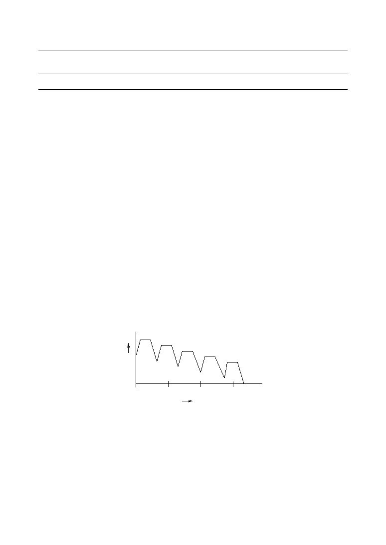
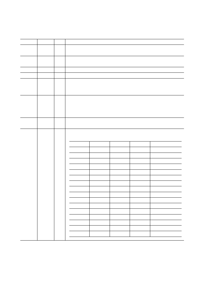
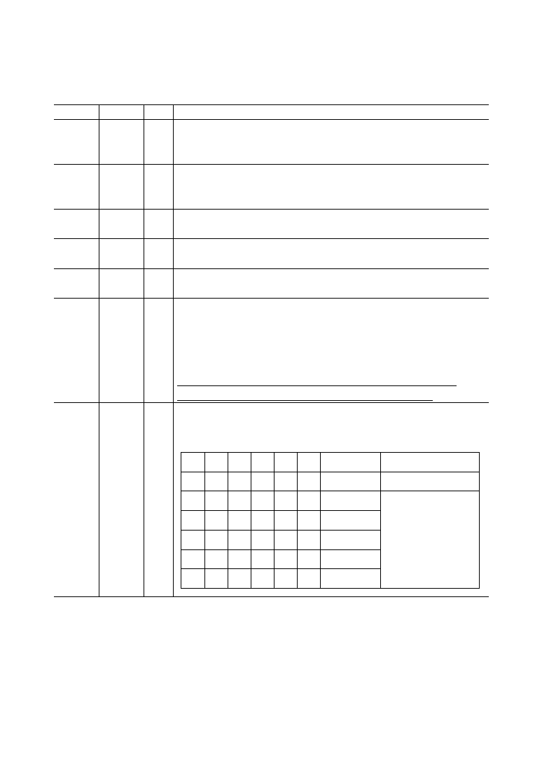
∑ SBC method:
The SBC method divides voice frequencies into five bands and codes the component for each of
the bands separately, as shown below.
° Semiconductor
MSM6789A/6789L
SBC Solid-State Recorder IC
Note:
This data sheet explains a stand-alone mode and a microcontroller interface mode, separately.
ch 1
ch 2
ch 3
ch 4
ch 5
1
2
3
0
kHz
Gain
f (Hz)
@f
s
=8.0 Hz

MSM6789A/6789L
° Semiconductor
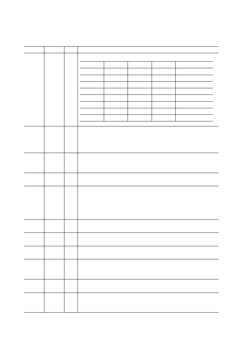
∑ Difference between MSM6789A and MSM6789L
*
Use ARAM which has no failed bits in its first 64 Kbits.
Parameter
Operating voltage
External memory
3.0 to 3.6 V
16 Mbits (max.)
4 Mbits (MSM66V84B)
MSM6789L
MSM6789A
4.5 to 5.5 V
General-purpose DRAM, 32 Mbits (max.)
4 Mbits (MSM6684B)
8 Mbits (MSM6685)
Serial register, 32 Mbits (max.)
1-Mbit DRAM (MSM514256B, MSM511000B)
4-Mbit DRAM (MSM514400C, MSM514100C)
16-Mbit DRAM (MSM511740CA, MSM5116100A)
ARAM*, 32 Mbits (max.)

° Semiconductor
MSM6789A/6789L
STAND-ALONE MODE
FEATURES
∑ SBC method
∑ Built-in 12-bit AD converter
∑ Built-in 12-bit DA converter
∑ Built-in microphone amplifier
∑ Built-in low-pass filter
Attenuation characteristics ≠40 dB/oct
∑ External memories
MSM6789A (5 V version)
General-purpose DRAM, 32 Mbits maximum (for variable messages)
1-Mbit DRAM : Can be directly driven (MSM514256B, MSM511000B)
4-Mbit DRAM : Can be directly driven (MSM514400C, MSM514100C)
16-Mbit DRAM : Can be directly driven (MSM5117400A, MSM5116100A)
ARAM, 32 Mbits maximum (for variable messages)
Note :Use the first 64 Kbits with no failed bits for the ARAM.
Serial register, 32 Mbits maximum (for variable messages)
4-Mbit serial register : Can be directly driven (MSM6684B)
8-Mbit serial register : Can be directly driven (MSM6685)
MSM6789L (3.3 V version)
Serial register, 16 Mbits maximum (for variable messages)
4-Mbit serial resister: Can be directly driven (MSM66V84B)
MSM6789A (5 V version) and MSM6789L (3.3 V version)
Serial voice ROM, 4 Mbits maximum (for fixed messages)
1-Mbit serial voice ROM : Can be directly driven (MSM6595A)
2-Mbit serial voice ROM : Can be directly driven (MSM6596A)
3-Mbit serial voice ROM : Can be directly driven (MSM6597A)
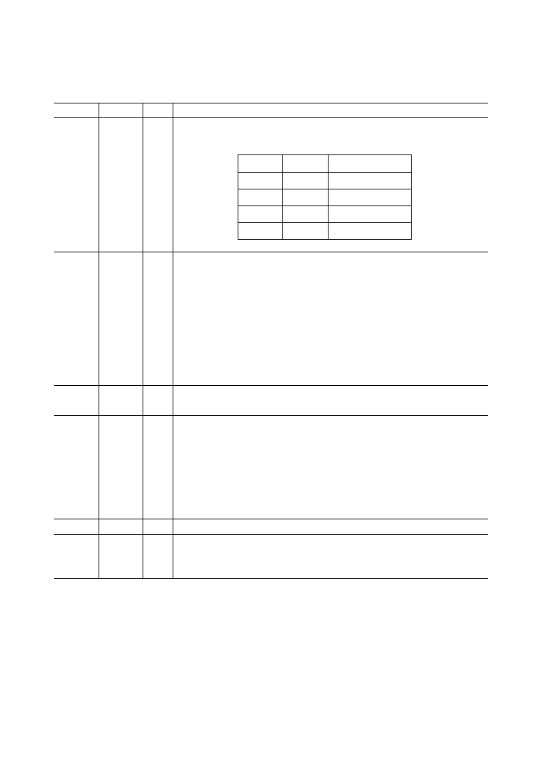
∑ Bit rate
10.0, 12.6, 16.0 kbps (at 8 kHz sampling freq.)
7.5, 9.5, 12.0 kbps (at 6 kHz sampling freq.)
∑ Maximum recording time (when one 8-Mbit serial register is connected)
13.8 minutes (for 10.0 kbps SBC)
18.4 minutes (for 7.5 kbps SBC)
11.0 minutes (for 12.6 kbps SBC)
14.6 minutes (for 9.5 kbps SBC)
8.6 minutes (for 16.0 kbps SBC)
11.5 minutes (for 12.0 kbps SBC)
∑ Number of phrases
63 phrases for variable messages
63 phrases for fixed messages
∑ Standard linear PCM playback or OKI nonlinear PCM playback can be selected.
∑ Voice triggered starting function (voice detect level can be set)
∑ Unvoiced-part elimination function (voice detect level can be set)
∑ Pausing function
∑ Master clock frequency:
6.0 MHz to 8.192 MHz
∑ Power supply voltage:
MSM6789A : Single 5 V power supply
MSM6789L : Single 3.3 V power supply
∑ Package options:
MSM6789A : 100-pin plastic QFP (QFP100-P-1420-BK) (Product name: MSM6789AGS-BK)
MSM6789L : 100-pin plastic QFP (QFP100-P-1420-BK) (Product name: MSM6789LGS-BK)
MSM6789A/6789L
° Semiconductor
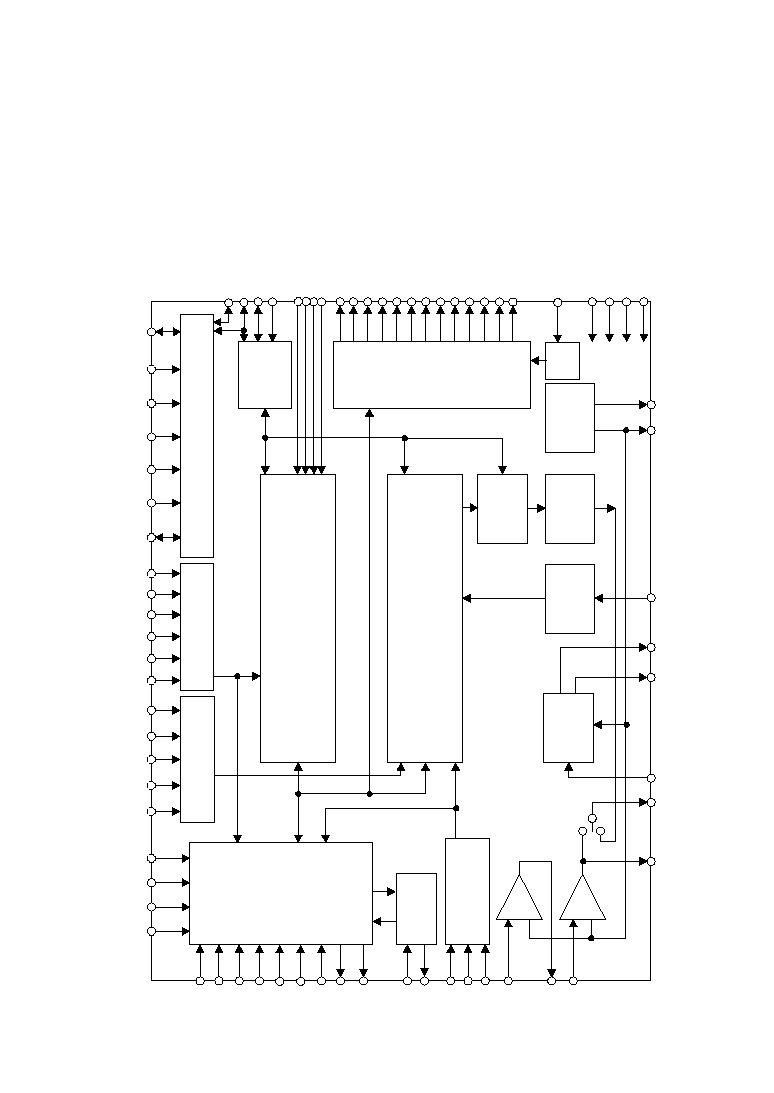
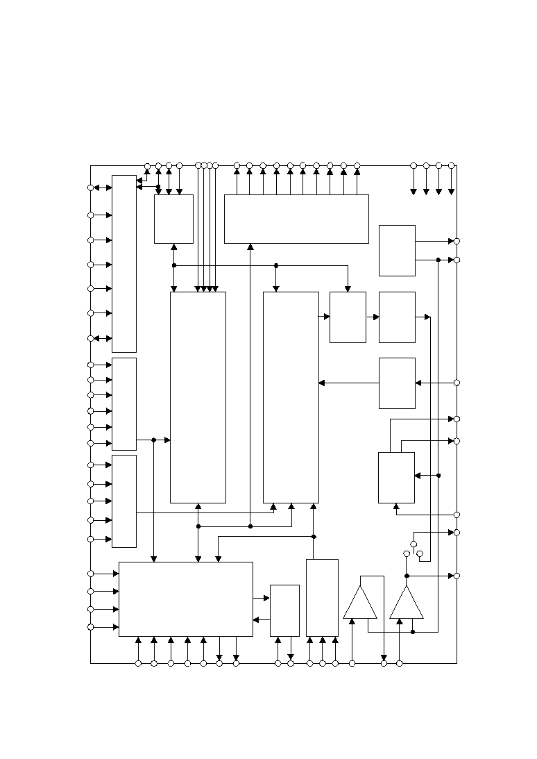
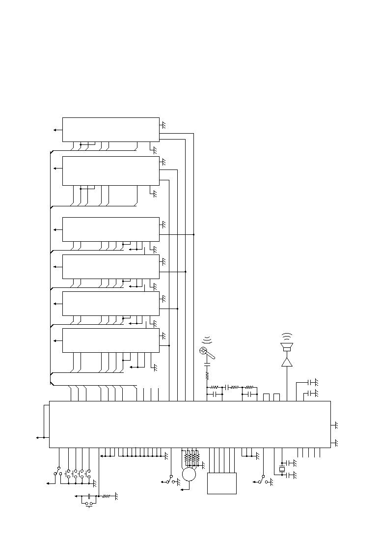
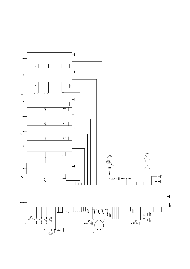
BLOCK DIAGRAM (for MSM6789A (5 V Version))
MCUM
RESET
PDWN
PDMD
VDS
ROM
MON
NAR
DEL
ST
SP
PAUSE
CA0
CA1
CA2
CA3
CA4
CA5
XT
XT
REC/
PLAY
BR0
MIN
MOUT
LIN
OSC
Latch
≠
+
≠
+
LOUT
AMON
FIN
AOUT
FOUT
ADIN
SG
SGC
A0(SADY)
A1(SADX)
A3(
SAS
)
A4(
RWCK
)
WE
CS1
CS2
CS3
CS4
RSEL1 RSEL2
DI/O
DROM
Data
I/O
Memory Controller
SBC
Analyzer/Synthesizer
LPF
12-bit
ADC
12-bit
DAC
SG
Circuit
DV
DD
AV
DD
DGND
AGND
Phrase Register
Address Controller
Timing
Controller
TEST
TEST
Test Circuit
TDT0 to TDT3 [DQ1 to DQ4]
TMD4
TST
TCK
SYNC
TDT4 to TDT7
TMD3
TMD0
to
BR1
A2(
TAS
)
PCM
Synthesizer
OSC
(RC)
LOWPWR
Compare
Circuit
VD0
VD1
VD2
VD3
CAS0
to
CAS7
RAS
A5 to A10
MSEL1 MSEL2
DRAM/
SR
4B/
1B
° Semiconductor
MSM6789A/6789L
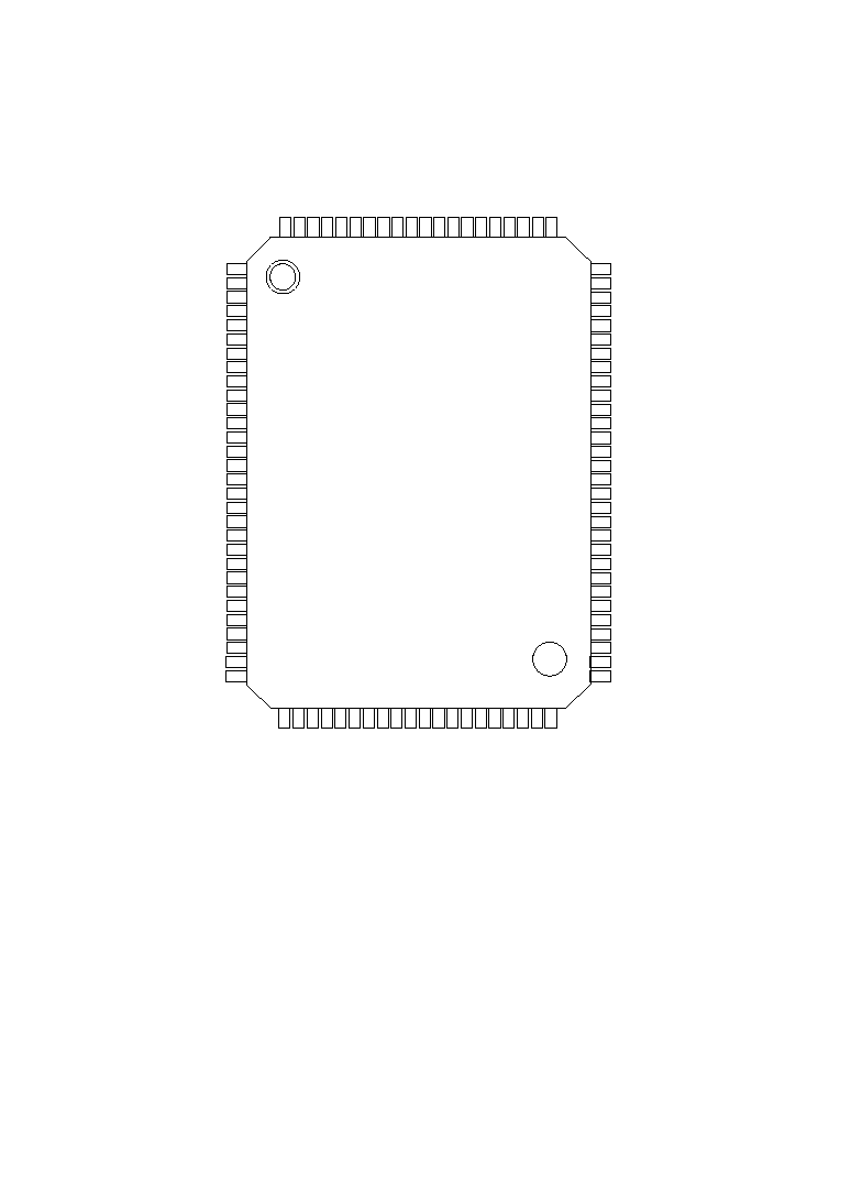
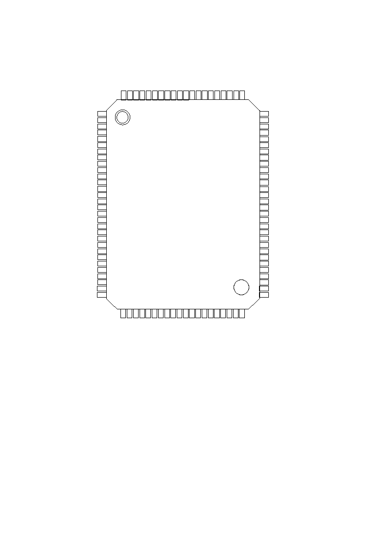
PIN CONFIGURATION (TOP VIEW) (for MSM6789A (5 V Version))
1
2
3
4
5
6
7
8
9
10
11
12
13
14
15
16
17
18
19
20
21
22
23
24
25
26
27
28
29
30
80
79
78
77
76
75
74
73
72
71
70
69
68
67
66
65
64
63
62
61
60
59
58
57
56
55
54
53
52
51
LOUT
SGC
SG
AV
DD
AMON
FIN
AOUT
FOUT
ADIN
DGND
ROM
VDS
TEST
BR1
BR0
MCUM
PAUSE
DEL
PDMD
A10
A9
A8
A7
A6
A5
TMD4
TMD3
TMD2
TMD1
TMD0
TDT7
TDT6
TDT5
TDT4
TDT3
TDT2
TDT1
TDT0
SYNC
TST
TCK
CA0
CA1
CA2
CA3
NC
CA5
A0 (SADY)
A1 (SADX)
A2 (TAS)
A3 (SAS)
A4 (RWCK)
WE
DI/O
MON
NAR
VD3
VD2
VD1
DRAM/SR
REC/PLAY
ST
SP
TEST
PDWN
RESET
VD0
MSEL2
MSEL1
RSEL2
RSEL1
DGND
AGND
MIN
MOUT
LIN
[DQ4]
[DQ3]
[DQ2]
[DQ1]
100
99
98
97
96
95
94
93
92
91
90
89
88
87
86
85
84
83
82
81
CS1
CS2
CS3
CS4
DROM
RAS
DV
DD
XT
XT
CAS0
CAS1
CAS2
CAS3
CAS4
CAS5
CAS6
CAS7
4B/
1B
31
32
33
34
35
36
37
38
39
40
41
42
43
44
45
46
47
48
49
50
LOWPWR
NC
CA4
NC
NC
NC
100-Pin Plastic QFP
( ) :
Pins for connecting serial voice ROM
[ ] :
Pins for connecting 4-bit • type DRAM
NC :
No-connection pin
MSM6789A/6789L
° Semiconductor
PIN DESCRIPTIONS (for MSM6789A (5 V Version))
Symbol
Type
Description
DV
DD
--
Digital power supply. Insert a bypass capacitor of 0.1
mF or more between this
pin and the DGND pin.
AV
DD
--
Analog power supply. Insert a bypass capacitor of 0.1
mF or more between this
pin and the AGND pin.
DGND
--
Digital ground.
AGND
--
Analog ground.
SG, SGC
--
Output for analog circuit reference voltage (signal ground).
MIN
Inverting input of the built-in OP amplifier. The non-inverting input pin is
internally connected to SG (signal ground).
LIN
I
MOUT
Output of the built-in OP amplifier for MIN and LIN.
LOUT
O
AMON
O
Connected to the LOUT pin in the recording mode and to the DA converter
output in the playback mode. This pin connects the built-in LPF input (FIN pin).
FIN
I
FOUT
O
Output of the built-in LPF. This pin connects the AD converter input (ADIN pin).
ADIN
I
Input of the built-in 12-bit AD converter.
AOUT
O
Output of the built-in LPF. This pin outputs playback waveforms and connects
an external speaker drive amplifier.
This pin selects whether memory to be connected externally is DRAM or serial register.
DRAM/SR
I
Low level
High level
This pin selects either 1-bit
• type DRAM or 4-bit • type DRAM.
4B/1B
I
A0 (SADY)
These pins connect to A0 and A1 of DRAM at the time of DRAM selection. They also
connect to SAD pin of serial register and serial voice ROM at the time of serial
register selection. These pins output leading addresses of read/write.
A1 (SADX)
O
This pin connects to A2 of DRAM at the time of DRAM selection. It also connects
to TAS pin of serial register and serial voice ROM at the time of serial register selection.
This pin is used to set serial addresses from the SADX and SADY pins into the
internal address counter of the serial register and serial voice ROM.
A2 (TAS)
O
This pin connects to A3 of DRAM at the time of DRAM selection. It also connects
to the SAS pin of the serial register and the SASX and SASY pins of the serial voice
ROM at the time of serial register selection. Clock pin to write serial addresses.
A3 (SAS)
O
This pin connects to A4 of DRAM at the time of DRAM selection. It also connects
to the RWCK pin of the serial register and the RDCK pin of the serial voice ROM at
the time of serial register selection. Clock pin to read data from and write data into
the serial register.
A4 (RWCK)
O
Input of the built-in LPF.
: Serial register
: DRAM
Low level
High level
: 1-bit
• type
: 4-bit
• type
A10-A5
O
This pin connects to pins A5-A10 of DRAM at the time of DRAM selection.
This pin outputs addresses of read/write.
Pin
90
47
40, 55
54
48, 49
53
51
52
50
46
45
43
42
44
66
88
79
78
77
76
75
1-6
° Semiconductor
MSM6789A/6789L
PIN DESCRIPTIONS (for MSM6789A (5 V Version)) (Continued)
Symbol
Type
Description
WE
O
Write Enable. This pin connects to the WE pin of the serial register and DRAM.
This pin selects either read or write mode.
DI/O
I/O
Data I/O. This pin connects to the DIN and DOUT pins of the serial register and
DRAM. This pin outputs write data and inputs read data.
DROM
I
Data ROM. This pin connects to the DOUT pin of the serial voice ROM.
RAS
O
This is a row address strobe pin of DRAM at the time of DRAM selection.
CAS0-
CAS7
O
These are the column address strobe pins of DRAM at the time of DRAM selection.
CAS7, an addresss output pin, is connected to pin A11 of DRAM at the time 16-Mbit
DRAM selection.
CS1
Chip Select. These pins connect to CS pin of the serial register and the CS (CS1,
CS2, CS3) pins of the serial voice ROM.
CS3
O
CS4
MSEL1
I
These pins select the capacity of the memory to be connected externally.
These pins select the number of DRAMs and serial registers to be connected externallly.
RSEL1
I
CS2
MSEL2
I
RSEL2
I
MSEL2
MSEL1
RSEL2
RSEL1
Memory capacity
L
L
L
L
1M
• 4
L
L
L
H
4M
• 1
L
L
H
L
1M
• 8
L
L
H
H
1M
• 4 + 4M • 1
L
H
L
L
4M
• 2
L
H
L
H
4M
• 2
L
H
H
L
4M
• 3
L
H
H
H
4M
• 3
H
L
L
L
4M
• 4
H
L
L
H
16M
• 1
H
L
H
L
4M
• 6
H
L
H
H
4M
• 6
H
H
L
L
4M
• 8
H
H
L
H
4M
• 8
H
H
H
L
16M
• 2
H
H
H
H
16M
• 2
∑ When DRAM is selected (DRAM/SR = High level)
Pin
74
73
85
89
93-100
81
83
84
58
82
59
56
57
MSM6789A/6789L
° Semiconductor
PIN DESCRIPTIONS (for MSM6789A (5 V Version)) (Continued)
Symbol
Type
Description
Mode Selection.
Low level : Stand-alone mode
High level : Microcontroller interface mode
PDWN
I
Power Down. When a low level is input, the MSM6789A goes to the power down
state. Unlike the RESET pin, this pin does not force the MSM6789A to be reset.
When a Low level is applied to this pin during recording operation, the MSM6789A
is halted, and will be maintained in the power down state while PDWN is low level.
After this pin is restored to a high level, postprocessing for recording will be performed.
Oscillator Connection. When an external clock is used, input the clock through
this pin. During the power down state, this pin must be set to the ground level.
XT
I
TEST
MSM6789A Test. Input a low level to the TEST pin and a high level to the TEST pin.
RSEL1
I
TEST
I
RSEL2
I
MSEL2
MSEL1
RSEL2
RSEL1
Memory capacity
L
L
L
L
4M
• 1
L
L
L
H
4M
• 2
L
L
H
L
4M
• 3
L
L
H
H
4M
• 4
L
H
L
L
8M
• 1
L
H
L
H
8M
• 2
L
H
H
L
8M
• 3
L
H
H
H
8M
• 4
∑ When serial register is selected (DRAM/SR = Low level)
MCUM
I
Oscillator Connection. When an external clock is used, this pin must be left
open.
XT
O
MSM6789A Test. This pin must be left open.
TMD3-TMD0
TDT7-TDT0
SYNC
I/O
Connect these pins to DQ1-DQ4 of DRAM at the time of 4-bit
• type DRAM
selection. Otherwise these pins must be left open as they are MSM6789A test pins.
TDT3-TDT0
[DQ4]-[DQ1]
I/O
MSM6789A Test. Input a low level signal.
TST
TCK
TMD4
I
This pin selects CAS-before-RAS refresh period of DRAM at the time of
power down when DRAM is selected.
Low level : 15 µs max.
High level : 125 µs max.
LOWPWR
I
A high input level causes the MSM6789A to be initialized and to go into the power
down state.
RESET
I
Pin
60
91
56
37
57
34
92
9-12
17-20
22
87
62
13-20
23
21
8
61

° Semiconductor
MSM6789A/6789L
PIN DESCRIPTIONS (for MSM6789A (5 V Version)) (Continued)
Symbol
Type
Description
ROM
I
Playback Operation. When set to low, this pin selects the record/playback
operation (only for the SBC method). When set to high, it selects the ROM playback
operation (for the SBC and PCM methods).
REC/PLAY
I
Recording mode or playback mode selection. This pin is invalid during
the ROM playback operation. When set to low, it selects the playback mode.
When set to high, it selects the recording mode.
ST
I
Start Playback. When a low-level pulse is applied to this pin, the record/playback
or ROM playback is started.
Playback Pause. When a low-level pulse is applied to this pin, the record/playback
or ROM operation is stopped temporarily.
PAUSE
I
DEL
I
Phrase Delection. When a low level pulse is applied to this pin, all phrase deletion
or specified phrase deletion can be performed according to the setting of pins CA0
through CA5,
ch00:All phrase deletion
ch01 to ch3F:Specified phrase deletion
After power up, be sure to input a RESET signal and then delete all phrases.
After completing this procedure, start the record/playback operation.
Desired Phrase Specification.
A total of 63 phrases can be specified indepedently for the record/playback operation
and the ROM playback operation.
CA0-CA5
I
SP
I
Stop Playback.When a low-level pulse is applied to this pin, the record/playback
or ROM playback is stopped.
CA5 CA4 CA3 CA2 CA1 CA0
Phrase No.
Remarks
L
L
L
L
L
L
ch00
All phrase deletion
L
L
L
L
L
H
ch01
.
.
.
.
.
.
.
.
.
.
.
.
.
.
.
ch02
L
L
L
L
H
L
.
.
.
H
H
H
H
H
L
ch3E
H
H
H
H
H
H
ch3F
A total of 63 phrases can
be used for both record
/playback and ROM
playback operation.
.
.
.
Pin
39
65
64
32
31
24-30
63
MSM6789A/6789L
° Semiconductor
PIN DESCRIPTIONS (for MSM6789A (5 V Version)) (Continued)
Symbol
Type
Description
BRO
BR1
I
Bit Rate Selection. This pin selects one of the following three types of bit rate (master
clock frequency f
OSC
= 8.192 MHz). This pin is invalid during the ROM playback operation.
PDMD
*1
I
Transition to the Power-down State.
VD0-VD3
I
These pins set the voice detect level for the voice triggered starting and unvoiced-part
elimination.
This pin selects the voice triggered starting or the unvoiced-part elimination.
VDS
I
BR1
BR0
Bit rate
L
L
16.0 kbps
L
H
H
H
L
H
12.6 kbps
10.0 kbps
Unused
Low level: The MSM6789A automatically goes to the power-down state, except
when the record/playback operation is performed.
High level: The MSM6789A automatically goes to the standby state, instead of the
power-down state, except when the record/playback operation
is performed. In this case, the MSM6789A can be placed in the
power-down state by setting the RESET or PDWN pin to a high level.
If an external circuit is used for the built-in LPF, this standby mode
must be selected by applying a high level to the PDMD pin.
This pin outputs a high level while the record/playback operation is being performed.
Output to indicate the enable or disable state of the operation for specifying a
phrase. When continuous ROM playback is performed, the next phrase can
be specified after the NAR pin goes to high positively.
MON
O
NAR
O
Pin
35
36
33
67-70
38
72
71
Voice triggered starting:
Note: When neither the voice triggered starting nor the unvoiced-part elimination is
used, input a Low level to VD0 to VD3.
Input a High level to the VDS pin. Then set the voice
detect level with VD0 to VD3 pins.
Unvoiced-part elimination:Input a Low level to the VDS pin. Then set the voice
detect level with VD0 to VD3 pins.
*1 When DRAM is selected, be sure to set the PDMD pin to a High level.
° Semiconductor
MSM6789A/6789L
ABSOLUTE MAXIMUM RATINGS (for MSM6789A (5 V Version))
Parameter
Symbol
Rating
Condition
Unit
Power supply voltage
V
DD
≠0.3 to +7.0
Ta=25∞C
V
Input voltage
V
IN
≠0.3 to V
DD
+0.3
Ta=25∞C
V
Storage temperature
T
STG
≠55 to +150
--
∞C
RECOMMENDED OPERATING CONDITIONS (for MSM6789A (5 V Version))
ELECTRICAL CHARACTERISTICS (for MSM6789A (5 V Version))
DC Characteristics
*1 Applies to all inputs excluding the XT pin.
*2 Applies to the XT pin.
*3 Applies to the input pins with pull-up resistor (ST, SP, PAUSE, DEL) excluding the XT pin.
*4 The record/playback operation must be performed at the power supply voltage of 4.5 to 5.5 V.
The MSM6789A operates at 3.5 to 5.5 V when the serial register is backed up.
Parameter
Symbol
Condition
High input voltage
V
IH
--
Low input voltage
V
IL
--
Min.
0.8
•V
DD
--
Typ.
--
--
Unit
V
V
Max.
--
0.2
•V
DD
High output voltage
V
OH
I
OH
=≠40
mA
V
DD
≠0.3
--
V
--
Low output voltage
V
OL
I
OL
=2 mA
--
--
V
0.45
High input current
*1
I
IH1
V
IH
=V
DD
--
--
mA
10
High input current
*2
I
IH2
V
IH
=V
DD
--
--
mA
20
Low input currcent
*1
I
IL1
V
IL
=GND
≠10
--
mA
--
Low input current
*2
I
IL2
V
IL
=GND
≠20
--
mA
--
Low input current
*3
I
IL3
V
IL
=GND
≠400
--
mA
≠20
Power down current
No load
Serial register connected
I
DDS1
--
--
mA
10
--
200
mA
--
I
DDS2
No load
DRAM connected
Operating current consumption
I
DD
f
OSC
=8 MHz, no load
--
20
mA
35
DV
DD
=AV
DD
=4.5 to 5.5 V
*4
DGND=AGND=0 V, Ta=0 to 70∞C
Parameter
Symbol
Range
Condition
Unit
Power supply voltage
V
DD
+3.5 to +5.5
*4
DGND=AGND=0 V
V
Operating temperature
T
op
0 to +70
--
∞C
Master clock frequencuy
f
OSC
6.0 to 8.192
--
MHz

MSM6789A/6789L
° Semiconductor
Parameter
Symbol
Condition
DA output relative error
V
DAE
no load
FIN admissible input voltage range
V
FIN
--
Min.
--
1
Typ.
--
--
Unit
mV
V
Max.
10
V
DD
≠1
FIN input impedance
R
FIN
1
--
M
W
--
Op-map open loop gain
G
OP
40
--
dB
--
Op-amp input impedance
R
INA
1
--
M
W
--
Op-amp load resistance
R
OUTA
200
--
k
W
--
AOUT load resistance
R
AOUT
50
--
k
W
--
FOUT load resistance
R
FOUT
50
--
k
W
--
--
f
IN
=0 to 4kHz
--
--
--
--
DV
DD
=AV
DD
=4.5 to 5.5 V
DGND=AGND=0 V Ta=0 to 70∞C
Analog Characteristics
° Semiconductor
MSM6789A/6789L
BLOCK DIAGRAM (for MSM6789L (3.3 V Version))
MCUM
RESET
PDWN
PDMD
VDS
ROM
MON
NAR
DEL
ST
SP
PAUSE
CA0
CA1
CA2
CA3
CA4
CA5
XT
XT
REC/
PLAY
BR0
MIN
MOUT
LIN
OSC
Latch
≠
+
≠
+
LOUT
AMON
FIN
AOUT
FOUT
ADIN
SG
SGC
SADY
SADX
SAS
RWCK
WE
CS1
CS2
CS3
CS4
RSEL1 RSEL2
DI/O
DROM
Data
I/O
Memory Controller
SBC
Analyzer/Synthesizer
LPF
12-bit
ADC
12-bit
DAC
SG
Circuit
DV
DD
AV
DD
DGND
AGND
Phrase Register
Address Controller
Timing
Controller
TEST
TEST
Test Circuit
TDT0 to TDT3
TMD4
TST
TCK
SYNC
TDT4 to TDT7
TMD3
TMD0
to
BR1
TAS
PCM
Synthesizer
Compare
Circuit
VD0
VD1
VD2
VD3
MSEL1 MSEL2
MSM6789A/6789L
° Semiconductor
PIN CONFIGURATION (TOP VIEW) (for MSM6789L (3.3 V Version))
1
2
3
4
5
6
7
8
9
10
11
12
13
14
15
16
17
18
19
20
21
22
23
24
25
26
27
28
29
30
80
79
78
77
76
75
74
73
72
71
70
69
68
67
66
65
64
63
62
61
60
59
58
57
56
55
54
53
52
51
LOUT
SGC
SG
AV
DD
AMON
FIN
AOUT
FOUT
ADIN
DGND
ROM
VDS
TEST
BR1
BR0
MCUM
PAUSE
DEL
PDMD
NC
NC
NC
NC
NC
NC
TMD4
TMD3
TMD2
TMD1
TMD0
TDT7
TDT6
TDT5
TDT4
TDT3
TDT2
TDT1
TDT0
SYNC
TST
TCK
CA0
CA1
CA2
CA3
NC
CA5
SADY
SADX
TAS
SAS
RWCK
WE
DI/O
MON
NAR
VD3
VD2
VD1
TEST
REC/PLAY
ST
SP
TEST
PDWN
RESET
VD0
MSEL2
MSEL1
RSEL2
RSEL1
DGND
AGND
MIN
MOUT
LIN
100
99
98
97
96
95
94
93
92
91
90
89
88
87
86
85
84
83
82
81
CS1
CS2
CS3
CS4
DROM
DV
DD
XT
XT
NC
NC
NC
NC
NC
NC
NC
NC
TEST
31
32
33
34
35
36
37
38
39
40
41
42
43
44
45
46
47
48
49
50
TEST
NC
CA4
NC
NC
NC
100-Pin Plastic QFP
NC :
No-connection pin
° Semiconductor
MSM6789A/6789L
PIN DESCRIPTIONS (for MSM6789L (3.3 V Version))
Symbol
Type
Description
DV
DD
--
Digital power supply. Insert a bypass capacitor of 0.1
mF or more between this
pin and the DGND pin.
AV
DD
--
Analog power supply. Insert a bypass capacitor of 0.1
mF or more between this
pin and the AGND pin.
DGND
--
Digital ground.
AGND
--
Analog ground.
SG, SGC
--
Output for analog circuit reference voltage (signal ground).
MIN
Inverting input of the built-in OP amplifier. The non-inverting input pin is
internally connected to SG (signal ground).
LIN
I
MOUT
Output of the built-in OP amplifier for MIN and LIN.
LOUT
O
AMON
O
Connected to the LOUT pin in the recording mode and to the DA converter
output in the playback mode. This pin connects the built-in LPF input (FIN pin).
FIN
I
FOUT
O
Output of the built-in LPF. This pin connects the AD converter input (ADIN pin).
ADIN
I
Input of the built-in 12-bit AD converter.
AOUT
O
Output of the built-in LPF. This pin outputs playback waveforms and connects
an external speaker drive amplifier.
SADY
They also connect to SAD pin of serial register and serial voice ROM. These pins
output leading addresses of read/write.
SADX
O
This pin connects to TAS pin of serial register and serial voice ROM.
This pin is used to set serial addresses from the SADX and SADY pins into the
internal address counter of the serial register and serial voice ROM.
TAS
O
This pin connects to the SAS pin of the serial register and the SASX and SASY pins
of the serial voice ROM. Clock pin to write serial addresses.
SAS
O
This pin connects to the RWCK pin of the serial register and the RDCK pin of the
serial voice ROM. Clock pin to read data from and write data into the serial register.
RWCK
O
Input of the built-in LPF.
Pin
90
47
40, 55
54
48, 49
53
51
52
50
46
45
43
42
44
79
78
77
76
75
WE
O
Write Enable. This pin connects to the WE pin of the serial register and DRAM.
This pin selects either read or write mode.
DI/O
I/O
Data I/O. This pin connects to the DIN and DOUT pins of the serial register and
DRAM. This pin outputs write data and inputs read data.
DROM
I
Data ROM. This pin connects to the DOUT pin of the serial voice ROM.
CS1
Chip Select. These pins connect to CS pin of the serial register and the CS (CS1,
CS2, CS3) pins of the serial voice ROM.
CS3
O
CS4
CS2
74
73
85
81
83
84
82
MSM6789A/6789L
° Semiconductor
PIN DESCRIPTIONS (for MSM6789L (3.3 V Version)) (Continued)
Symbol
Type
Description
MSEL1
I
These pins select the capacity of the memory to be connected externally.
These pins select the number of and serial registers to be connected externallly.
MSEL2
I
Pin
58
59
Mode Selection.
Low level : Stand-alone mode
High level : Microcontroller interface mode
PDWN
I
Power Down. When a low level is input, the MSM6789L goes to the power down
state. Unlike the RESET pin, this pin does not force the MSM6789L to be reset.
When a Low level is applied to this pin during recording operation, the MSM6789L
is halted, and will be maintained in the power down state while PDWN is low level.
After this pin is restored to a high level, postprocessing for recording will be performed.
Oscillator Connection. When an external clock is used, input the clock through
this pin. During the power down state, this pin must be set to the ground level.
XT
I
TEST
MSM6789L Test. Input a low level to the TEST pin and a high level to the TEST pin.
RSEL1
I
TEST
I
RSEL2
I
MSEL2
MSEL1
RSEL2
RSEL1
Memory capacity
L
L
L
L
4M
• 1
L
L
L
H
4M
• 2
L
L
H
L
4M
• 3
L
L
H
H
4M
• 4
MCUM
I
Oscillator Connection. When an external clock is used, this pin must be left
open.
XT
O
MSM6789L Test. This pin must be left open.
TMD3-TMD0
TDT7-TDT0
SYNC
I/O
These pins must be left open as they are MSM6789L test pins.
TDT3-TDT0
I/O
MSM6789L Test. Input a low level signal.
TST
TCK
TMD4
I
A high input level causes the MSM6789L to be initialized and to go into the power
down state.
RESET
I
60
91
56
37
57
34
92
9-12
17-20
22
62
13-20
23
21
8
61
° Semiconductor
MSM6789A/6789L
PIN DESCRIPTIONS (for MSM6789L (3.3 V Version)) (Continued)
Symbol
Type
Description
ROM
I
Playback Operation. When set to low, this pin selects the record/playback
operation (only for the SBC method). When set to high, it selects the ROM playback
operation (for the SBC and PCM methods).
REC/PLAY
I
Recording mode or playback mode selection. This pin is invalid during
the ROM playback operation. When set to low, it selects the playback mode.
When set to high, it selects the recording mode.
ST
I
Start Playback. When a low-level pulse is applied to this pin, the record/playback
or ROM playback is started.
Playback Pause. When a low-level pulse is applied to this pin, the record/playback
or ROM operation is stopped temporarily.
PAUSE
I
DEL
I
Phrase Delection. When a low level pulse is applied to this pin, all phrase deletion
or specified phrase deletion can be performed according to the setting of pins CA0
through CA5,
ch00:All phrase deletion
ch01 to ch3F:Specified phrase deletion
After power up, be sure to input a RESET signal and then delete all phrases.
After completing this procedure, start the record/playback operation.
Desired Phrase Specification.
A total of 63 phrases can be specified indepedently for the record/playback operation
and the ROM playback operation.
CA0-CA5
I
SP
I
Stop Playback.When a low-level pulse is applied to this pin, the record/playback
or ROM playback is stopped.
CA5 CA4 CA3 CA2 CA1 CA0
Phrase No.
Remarks
L
L
L
L
L
L
ch00
All phrase deletion
L
L
L
L
L
H
ch01
.
.
.
.
.
.
.
.
.
.
.
.
.
.
.
ch02
L
L
L
L
H
L
.
.
.
H
H
H
H
H
L
ch3E
H
H
H
H
H
H
ch3F
A total of 63 phrases can
be used for both record
/playback and ROM
playback operation.
.
.
.
Pin
39
65
64
32
31
24-30
63
MSM6789A/6789L
° Semiconductor
PIN DESCRIPTIONS (for MSM6789L (3.3 V Version)) (Continued)
Symbol
Type
Description
BRO
BR1
I
Bit Rate Selection. This pin selects one of the following three types of bit rate (master
clock frequency f
OSC
= 8.192 MHz). This pin is invalid during the ROM playback operation.
PDMD
*1
I
Transition to the Power-down State.
VD0-VD3
I
These pins set the voice detect level for the voice triggered starting and unvoiced-part
elimination.
This pin selects the voice triggered starting or the unvoiced-part elimination.
VDS
I
BR1
BR0
Bit rate
L
L
16.0 kbps
L
H
H
H
L
H
12.6 kbps
10.0 kbps
Unused
Low level: The MSM6789L automatically goes to the power-down state, except
when the record/playback operation is performed.
High level: The MSM6789L automatically goes to the standby state, instead of the
power-down state, except when the record/playback operation
is performed. In this case, the MSM6789L can be placed in the
power-down state by setting the RESET or PDWN pin to a high level.
If an external circuit is used for the built-in LPF, this standby mode
must be selected by applying a high level to the PDMD pin.
This pin outputs a high level while the record/playback operation is being performed.
Output to indicate the enable or disable state of the operation for specifying a
phrase. When continuous ROM playback is performed, the next phrase can
be specified after the NAR pin goes to high positively.
MON
O
NAR
O
Pin
35
36
33
67-70
38
72
71
Voice triggered starting:
Note: When neither the voice triggered starting nor the unvoiced-part elimination is
used, input a Low level to VD0 to VD3.
Input a High level to the VDS pin. Then set the voice
detect level with VD0 to VD3 pins.
Unvoiced-part elimination:Input a Low level to the VDS pin. Then set the voice
detect level with VD0 to VD3 pins.
*1 When DRAM is selected, be sure to set the PDMD pin to a High level.

° Semiconductor
MSM6789A/6789L
ABSOLUTE MAXIMUM RATINGS (for MSM6789L (3.3 V Version))
RECOMMENDED OPERATING CONDITIONS (for MSM6789L (3.3 V Version))
Parameter
Symbol
Range
Condition
Unit
Power supply voltage
V
DD
+3.0 to +3.6
DGND=AGND=0 V
V
Operating temperature
T
op
0 to +70
--
∞C
Master clock frequencuy
f
OSC
6.0 to 8.192
--
MHz
ELECTRICAL CHARACTERISTICS (for MSM6789L (3.3 V Version))
DC Characteristics
Parameter
Symbol
Condition
High input voltage
V
IH
--
Low input voltage
V
IL
--
Min.
0.85
•V
DD
--
Typ.
--
--
Unit
V
V
Max.
--
0.15
•V
DD
High output voltage
V
OH
I
OH
=≠40
mA
V
DD
≠0.3
--
V
--
Low output voltage
V
OL
I
OL
=2 mA
--
--
V
0.45
High input current
*1
I
IH1
V
IH
=V
DD
--
--
mA
10
High input current
*2
I
IH2
V
IH
=V
DD
--
--
mA
20
Low input currcent
*1
I
IL1
V
IL
=GND
≠10
--
mA
--
Low input current
*2
I
IL2
V
IL
=GND
≠20
--
mA
--
Low input current
*3
I
IL3
V
IL
=GND
≠400
--
mA
≠20
Power down current
No load
Serial register connected
I
DDS1
--
--
mA
10
--
200
mA
--
I
DDS2
No load
DRAM connected
Operating current consumption
I
DD
f
OSC
=8 MHz, no load
--
20
mA
35
DV
DD
=AV
DD
=3.0 to 3.6 V
DGND=AGND=0 V, Ta=0 to 70∞C
*1 Applies to all inputs excluding the XT pin.
*2 Applies to the XT pin.
*3 Applies to the input pins with pull-up resistor (ST, SP, PAUSE, DEL) excluding the XT pin.
Parameter
Symbol
Rating
Condition
Unit
Power supply voltage
V
DD
≠0.3 to +7.0
Ta=25∞C
V
Input voltage
V
IN
≠0.3 to V
DD
+0.3
Ta=25∞C
V
Storage temperature
T
STG
≠55 to +150
--
∞C

MSM6789A/6789L
° Semiconductor
Parameter
Symbol
Condition
DA output relative error
V
DAE
no load
FIN admissible input voltage range
V
FIN
--
Min.
--
1
Typ.
--
--
Unit
mV
V
Max.
20
V
DD
≠1
FIN input impedance
R
FIN
1
--
M
W
--
Op-map open loop gain
G
OP
40
--
dB
--
Op-amp input impedance
R
INA
1
--
M
W
--
Op-amp load resistance
R
OUTA
400
--
k
W
--
AOUT load resistance
R
AOUT
100
--
k
W
--
FOUT load resistance
R
FOUT
100
--
k
W
--
--
f
IN
=0 to 4kHz
--
--
--
--
DV
DD
=AV
DD
=3.0 to 3.6 V
DGND=AGND=0 V Ta=0 to 70∞C
Analog Characteristics
° Semiconductor
MSM6789A/6789L
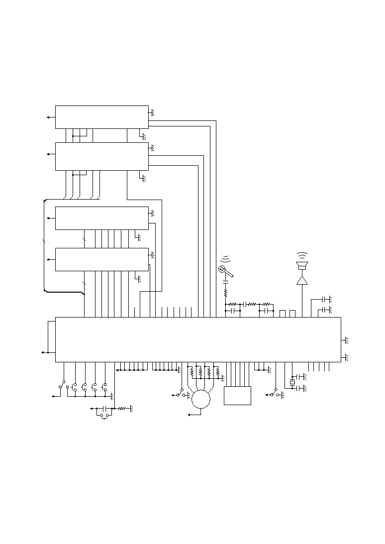
APPLICATION CIRCUITS (for MSM6789A (5 V version))
This is an application circuit example when the MSM6789A is used in stand-alone mode with four
8-Mbit serial registers and two 2-Mbit serial voice ROMs.
+
+
SG
SGC
AOUT
ADIN
FOUT
FIN
AMON
LOUT
LIN
MOUT
MIN
CS4
CS3
CS2
CS1
DROM
DI/O
WE
RWCK
TAS
SADY
SAS
SADX
SADX
SAD
SAS
SAS
TAS
TAS
RWCK
RWCK
WE
WE
DI/O
DIN
DOUT
TEST
RS/A
CS
V
SS
V
CC
SADX
SADX
SAS
SASX
TAS
TAS
RWCK
RDCK
DOUT
TEST
CS1
CS2
V
CC
SADY
SADY
SASY
DROM
V
SS
Speaker drive amplifier
CA5
CA4
CA3
CA2
CA1
CA0
SW
Phrase
Selection
RECORDER IC MSM6789A
8M Serial Register MSM6685
MSM6685
MSM6685
MSM6685
2M Serial Voice ROM
MSM6596A-XXX
MSM6596A-XXX
AV
DD
DV
DD
REC/
PLAY
PAUSE
SP
ST
DEL
ROM
TST
TCK
TMD4
XT
XT
8.192 MHz
AGND
DGND
RFSH
NC
RESET
MSEL1
VDS
DV
DD
VD0
VD3 VD2 VD1
MON
NAR
TDT0-7
TMD0-3
SYNC
TEST
MCUM LOWPWR TEST
BR1 PDMD
4B/
1B
DRAM/
SR
BR0
HEX SW
PDWN
RAS
A5-A10
CAS0
-
CAS7
MSEL2
RSEL1 RSEL2
Circuit
1
:
Application circuit in stand-alone mode with 8-Mbit serial registers
and 2-Mbit serial voice ROMs.
MSM6789A/6789L
° Semiconductor
REC/
PLAY
DEL
ST
SP
PAUSE
PDWN
RSEL1
TEST
MCUM
VDS
LOWPWR
VD3
VD2
VD1
VD0
SG
SGC
AOUT
ADIN
FOUT
FIN
AMON
LOUT
LIN
MOUT
MIN
CS4
CS3
CS2
CS1
CAS4
DI/O
WE
A4(
RWCK
)
A2(
TAS
)
A0(SADY)
A3(
SAS
)
A1(SADX)
AV
DD
DV
DD
CAS
V
SS
V
CC
SADX
SADX
SAS
SASX
TAS
TAS
RWCK
RDCK
DOUT
TEST
CS1
CS2
V
CC
SADY
SADY
SASY
DROM
V
SS
RECORDER
IC MSM6789A
4-Mbit DRAM MSM514100C
2M Serial Voice ROM
MSM6596A-XXX
MSM6596A-XXX
BR0 BR1 PDMD
RESET
MON
NAR
TDT0-7
TMD0-3
+
+
Speaker drive amplifier
DGND
AGND
TST
TCK
TMD4
XT
XT
8.192 MHz
ROM
HEX SW
MSEL2 MSEL1
RSEL2
CAS5
CAS6
CAS7
DROM
CAS0
CAS1
CAS2
CAS3
A5
A6
A7
RAS
A8
A9
A10
DIN
WE
A4
A2
A0
A1
DOUT
A5
A6
A7
RAS
A8
A9
A10
A3
DI/O
WE
A4
A2
A0
A1
A5
A6
A7
A8
A9
A10
A3
MSM514100C
MSM514100C
MSM514100C
V
CC
V
CC
V
CC
CAS
V
SS
CAS
V
SS
CAS
V
SS
SYNC
CA0
CA1
CA2
CA3
SW
Phrase
Selection
TEST
DRAM/
SR
4B/
1B
CA4
CA5
Circuit
2
:
Application circuit in stand-alone mode with 4-Mbit DRAMs and
2-Mbit serial voice ROMs.
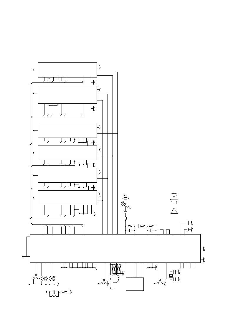
APPLICATION CIRCUITS (for MSM6789A (5 V version)) (Continued)
This is an application circuit example when the MSM6789A is used in stand-alone mode with four
4-Mbit DRAMs (1-bit • type) and two 2-Mbit serial voice ROMs.
° Semiconductor
MSM6789A/6789L
APPLICATION CIRCUITS (for MSM6789A (5 V version)) (Continued)
This is an application circuit example when the MSM6789A is used in stand-alone mode with one
4-Mbit DRAM, four 1-Mbit DRAMs (1-bit • type) and two 2-Mbit serial voice ROMs.
PDWN TEST
MCUM
TEST
VD3
VD2
VD1
VD0
SG
SGC
AOUT
ADIN
FOUT
FIN
AMON
LOUT
LIN
MOUT
MIN
CS4
CS3
CS2
CS1
CAS4
DI/O
WE
AV
DD
DV
DD
CAS
V
SS
V
CC
A1(SADX)
SADX
A3(
SAS
)
SASX
A2(
TAS
)
TAS
A4(
RWCK
)
RDCK
DOUT
TEST
CS1
CS2
V
CC
A0(SADY)
SADY
SASY
DROM
V
SS
RECORDER IC MSM6789A
1-Mbit DRAM MSM511000B
2M Serial Voice ROM
MSM6596A-XXX
MSM6596A-XXX
BR0 BR1 PDMD
REC/
PLAY
DEL
ST
SP
PAUSE
RESET
TST
TCK
TMD4
MON
NAR
TDT0-7
TMD0-3
XT
XT
8.192 MHz
+
+
Speaker drive amplifier
DGND
AGND
ROM
HEX SW
MSEL2
RSEL1
RSEL2
VDS
CA0
CA1
CA2
CA3
SW
Phrase
Selection
CAS5
CAS6
CAS7
DROM
CAS0
CAS1
CAS2
CAS3
RAS
A0~A9
A0~A
MSM511000B
MSM511000B
MSM511000B
MSEL1
A0-A10
V
CC
CAS
V
SS
WE DIN
DOUT
RAS
A0-A4
A0-A10
11
10
10
10
10
5
4-Mbit DRAM MSM514100C
CAS
V
SS
CAS
V
SS
CAS
V
SS
V
CC
V
CC
V
CC
SYNC
DRAM/
SR
LOWPWR
4B/
1B
CA4
CA5
Circuit 3 :
Application circuit in stand-alone mode with 4-Mbit DRAMs,
1-Mbit DRAMs and 2-Mbit serial voice ROMs.
MSM6789A/6789L
° Semiconductor
APPLICATION CIRCUITS (for MSM6789A (5 V version)) (Continued)
This is an application circuit example when the MSM6789A is used in stand-alone mode with two
16-Mbit DRAMs (1-bit • type) and two 2-Mbit serial voice ROMs.
MCUM
VDS
TEST
VD3
VD2
VD1
VD0
SG
SGC
AOUT
ADIN
FOUT
FIN
AMON
LOUT
LIN
MOUT
MIN
CS4
CS3
CS2
CS1
CAS4
DI/O
WE
AV
DD
DV
DD
CAS
V
SS
V
CC
A1(SADX)
SADX
A3(
SAS
)
SASX
A2(
TAS
)
TAS
A4(
RWCK
)
RDCK
DOUT
TEST
CS1
CS2
V
CC
A0(SADY)
SADY
SASY
DROM
V
SS
RECORDER IC MSM6789A
16-Mbit DRAM MSM5116100A
2M Serial Voice ROM
MSM6596A-XXX
MSM6596A-XXX
BR0 BR1 PDMD
REC/
PLAY
DEL
ST
SP
PAUSE
RESET
TST
TCK
TMD4
MON
NAR
TDT0-7
TMD0-3
XT
XT
8.192 MHz
+
+
Speaker Drive Amplifier
DGND
AGND
ROM
HEX SW
PDWN TEST
MSEL2 MSEL1
RSEL1
RSEL2
CA0
CA1
CA2
CA3
SW
Phrase
Slection
CAS5
CAS6
CAS7
DROM
CAS0
CAS1
CAS2
CAS3
RAS
DIN
WE
DOUT
A0-A10
A11
RAS
A0-A10
MSM5116100A
V
CC
CAS
V
SS
11
A0-A10
11
A0-A10
5
A0-A4
SYNC
CA4
CA5
DRAM/
SR
4B/
1B
LOWPWR
Circuit
4
:
Application circuit in stand-alone mode with 16-
Mbit DRAMs, and 2-Mbit serial voice ROMs.
° Semiconductor
MSM6789A/6789L
APPLICATION CIRCUITS (for MSM6789A (5 V version)) (Continued)
This is an application circuit example when the MSM6789A is used in stand-alone mode with four
4-Mbit DRAMs (4-bit • type) and two 2-Mbit serial voice ROMs.
PDWN
RSEL1
TEST
MCUM
VDS
LOWPWR
VD3
VD2
VD1
VD0
SG
SGC
AOUT
ADIN
FOUT
FIN
AMON
LOUT
LIN
MOUT
MIN
CS4
CS3
CS2
CS1
CAS4
DI/O
WE
AV
DD
DV
DD
A1(SADX)
SADX
A3(
SAS
)
SASX
A2(
TAS
)
TAS
A4(
RWCK
)
RDCK
DOUT
TEST
CS1
CS2
V
CC
A0(SADY)
SADY
SASY
V
SS
RECORDER IC MSM6789A
2M Serial Voice ROM
MSM6596A-XXX
MSM6596A-XXX
BR0 BR1 PDMD
REC/
PLAY
DEL
ST
SP
PAUSE
RESET
MON
NAR
TDT4-7
TMD0-3
+
+
Speaker Drive Amplifier
DGND
AGND
TST
TCK
TMD4
XT
XT
8.192 MHz
ROM
HEX SW
MSEL2 MSEL1
RSEL2
CAS5
CAS6
CAS7
DROM
CAS0
CAS1
CAS2
CAS3
[TDT0]DQ1
[TDT1]DQ2
[TDT2]DQ3
RAS
[TDT3]DQ4
A0-A9
A10
MSM514400C
MSM514400C
V
CC
V
CC
CAS
V
SS
CAS
V
SS
CA0
CA1
CA2
CA3
SW
Phrace
Slection
TEST
DRAM/
SR
4B/
1B
CAS
V
SS
V
CC
4-Mbit DRAM MSM514400C
WE
RAS
A0~A9
MSM514400C
V
CC
CAS
V
SS
DQ1
DQ2
DQ3
DQ4
10
10
10
10
5
A0-A4
V
CC
SYNC
CA4
CA5
OE
Circuit
5
:
Application circuit in stand-alone mode with 4-Mbit DRAMs and
2-Mbit serial voice ROMs.
MSM6789A/6789L
° Semiconductor
APPLICATION CIRCUITS (for MSM6789A (5 V version)) (Continued)
This is an application circuit example when the MSM6789A is used in stand-alone mode with one
4-Mbit DRAM, four 1-Mbit DRAMs (4-bit • type), and two 2-Mbit serial voice ROMs.
MCUM
TEST
VD3
VD2
VD1
VD0
SG
SGC
AOUT
ADIN
FOUT
FIN
AMON
LOUT
LIN
MOUT
MIN
CS4
CS3
CS2
CS1
CAS4
DI/O
WE
AV
DD
DV
DD
V
CC
A1(SADX)
SADX
A3(
SAS
)
SASX
A2(
TAS
)
TAS
A4(
RWCK
)
RDCK
DOUT
TEST
CS1
CS2
V
CC
A0(SADY)
SADY
SASY
DROM
V
SS
RECORDER IC MSM6789A
1-Mbit DRAM MSM514256B
2M Serial Voice ROM
MSM6596A-XXX
MSM6596A-XXX
BR0 BR1 PDMD
REC/
PLAY
DEL
ST
SP
PAUSE
RESET
TST
TCK
TMD4
MON
NAR
TDT4-7
TMD0-3
XT
XT
8.192 MHz
+
+
Speaker drive amplifier
DGND
AGND
ROM
HEX SW
MSEL2
RSEL1
RSEL2
VDS
CA0
CA1
CA2
CA3
SW
Phrase
selection
CAS5
CAS6
CAS7
DROM
CAS0
CAS1
CAS2
CAS3
RAS
A0-A8
MSM514256B
MSM514256B
MSM514256B
MSEL1
A0-A9
V
CC
CAS
V
SS
WE
RAS
A0-A4
A0-A9
10
9
99
9
5
4-Mbit DRAM MSM514400C
CAS
V
SS
CAS
V
SS
CAS
V
SS
V
CC
V
CC
V
CC
PDWN TEST DRAM/
SR
LOWPWR
A10
[TDT0]DQ1
[TDT1]DQ2
[TDT2]DQ3
[TDT3]DQ4
DQ1
DQ2
DQ3
DQ4
4B/
1B
CAS
V
SS
CA4
CA5
OE
SYNC
Circuit
6
:
Application circuit in stand-alone mode with 4-Mbit DRAMs,
1-Mbit DRAM, and 2M-bit serial voice ROMs.
° Semiconductor
MSM6789A/6789L
APPLICATION CIRCUITS (for MSM6789A (5 V version)) (Continued)
This is an application circuit example when the MSM6789A is used in stand-alone mode with two
16-Mbit DRAMs (4-bit • type) and two 2-Mbit serial voice ROMs.
MCUM
VDS
TEST
VD3
VD2
VD1
VD0
SG
SGC
AOUT
ADIN
FOUT
FIN
AMON
LOUT
LIN
MOUT
MIN
CS4
CS3
CS2
CS1
CAS4
DI/O
WE
AV
DD
DV
DD
CAS
V
SS
V
CC
A1(SADX)
SADX
A3(
SAS
)
SASX
A2(
TAS
)
TAS
A4(
RWCK
)
RDCK
DOUT
TEST
CS1
CS2
V
CC
A0(SADY)
SADY
SASY
DROM
V
SS
RECORDER IC MSM6789A
16-Mbit DRAM MSM5117400A
2M Serial Voice ROM
MSM6596A-XXX
MSM6596A-XXX
BR0 BR1 PDMD
REC/
PLAY
DEL
ST
SP
PAUSE
RESET
TST
TCK
TMD4
MON
NAR
TDT4-7
TMD0-3
XT
XT
8.192 MHz
+
+
Speaker drive amplifier
DGND
AGND
ROM
HEX SW
PDWN TEST
MSEL2 MSEL1
RSEL1
RSEL2
CA0
CA1
CA2
CA3
SW
Phrase
selection
CAS5
CAS6
CAS7
DROM
CAS0
CAS1
CAS2
CAS3
RAS
WE
RAS
MSM5117400A
V
CC
CAS
V
SS
A0-A10
A0-A10
11
A0-A10
11
A0-A10
5
A0-A4
DRAM/
SR
4B/
1B
[TDT0]DQ1
[TDT1]DQ2
[TDT2]DQ3
[TDT3]DQ4
DQ1
DQ2
DQ3
DQ4
LOWPWR
SYNC
CA4
CA5
OE
Circuit
7
:
Application circuit in stand-alone mode with 16-Mbit
DRAMs and 2-Mbit serial voice ROMs.
MSM6789A/6789L
° Semiconductor
APPLICATION CIRCUITS (for MSM6789L (3.3 V Version))
This is an application circuit example when the MSM6789L is used in stand-alone mode with four
4-Mbit serial registers and two 2-Mbit serial voice ROMs.
+
+
SG
SGC
AOUT
ADIN
FOUT
FIN
AMON
LOUT
LIN
MOUT
MIN
CS4
CS3
CS2
CS1
DROM
DI/O
WE
RWCK
TAS
SADY
SAS
SADX
SADX
SAD
SAS
SAS
TAS
TAS
RWCK
RWCK
WE
WE
DI/O
DIN
DOUT
TEST
RS/A
CS
V
SS
V
CC
SADX
SADX
SAS
SASX
TAS
TAS
RWCK
RDCK
DOUT
TEST
CS1
CS2
V
CC
SADY
SADY
SASY
DROM
V
SS
Speaker drive amplifier
CA5
CA4
CA3
CA2
CA1
CA0
SW
Phrase
Selection
RECORDER IC MSM6789L
4M Serial Register MSM66V84B
MSM66V84B
MSM66V84B
MSM66V84B
2M Serial Voice ROM
MSM6596A-XXX
MSM6596A-XXX
AV
DD
DV
DD
REC/
PLAY
PAUSE
SP
ST
DEL
ROM
TST
TCK
TMD4
XT
XT
8.192 MHz
AGND
DGND
RFSH
NC
RESET
MSEL1
VDS
DV
DD
VD0
VD3 VD2 VD1
MON
NAR
TDT0-7
TMD0-3
SYNC
TEST
MCUM TEST
BR1 PDMD
BR0
HEX SW
PDWN
MSEL2
RSEL1 RSEL2
Circuit
8
:
Application circuit in stand-alone mode with 4-Mbit serial
registers and 2-Mbit serial voice ROMs.

° Semiconductor
MSM6789A/6789L
MICROCONTROLLER INTERFACE MODE
FEATURES
∑ SBC method
∑ Built-in 12-bit AD converter
∑ Built-in 12-bit DA converter
∑ Built-in microphone amplifier
∑ Built-in low-pass filter
Attenuation characteristics ≠40 dB/oct
∑ External memories
MSM6789A (5 V version)
General-purpose DRAM, 32 Mbits maximum (for variable messages)
1-Mbit DRAM : Can be directly driven (MSM514256B, MSM511000B)
4-Mbit DRAM : Can be directly driven (MSM514400C, MSM514100C)
16-Mbit DRAM : Can be directly driven (MSM5117400A, MSM5116100A)
ARAM, 32 Mbits maximum (for variable messages)
Note: Use the first 64 Kbits with no failed bits for the ARAM.
Serial register, 32 Mbits maximum (for variable messages)
4-Mbit serial register : Can be directly driven (MSM6684B)
8-Mbit serial register : Can be directly driven (MSM6685)
MSM6789L (3.3 V version)
Serial register, 16 Mbits maximum (for variable messages)
4-Mbit serial register: Can be directly driven (MSM66V84B)
MSM6789A (5 V version) and MSM6789L (3.3 V version)
Serial voice ROM, 4 Mbits maximum (for fixed messages)
1-Mbit serial voice ROM : Can be directly driven (MSM6595A)
2-Mbit serial voice ROM : Can be directly driven (MSM6596A)
3-Mbit serial voice ROM : Can be directly driven (MSM6597A)
∑ Bit rate
10.0, 12.6, 16.0 kbps (at 8 kHz sampling freq.)
7.5, 9.5, 12.0 kbps (at 6 kHz sampling freq.)
∑ Maximum recording time (when one 8-Mbit serial register is connected)
13.8 minutes (for 10.0 kbps SBC)
18.4 minutes (for 7.5 kbps SBC)
11.0 minutes (for 12.6 kbps SBC)
14.6 minutes (for 9.5 kbps SBC)
8.6 minutes (for 16.0 kbps SBC)
11.5 minutes (for 12.0 kbps SBC)
∑ Number of phrases
63 phrases for variable messages
255 phrases for fixed messages
∑ Standard linear PCM playback or OKI nonlinear PCM playback can be selected.
∑ Voice triggered starting function (voice detect level can be set)
∑ Uuvoiced-part elimination function (voice detect level can be set)
∑ Pausing function
∑ Master clock frequency:
6.0 MHz to 8.192 MHz
∑ Power supply voltage:
MSM6789A:
Single 5 V power supply
MSM6789L:
Single 3.3 V power supply
∑ Package options:
MSM6789A:
100-pin plastic QFP (QFP100-P-1420-BK) (Product name: MSM6789AGS-BK)
MSM6789L:
100-pin plastic QFP (QFP100-P-1420-BK) (Product name: MSM6789LGS-BK)
MSM6789A/6789L
° Semiconductor
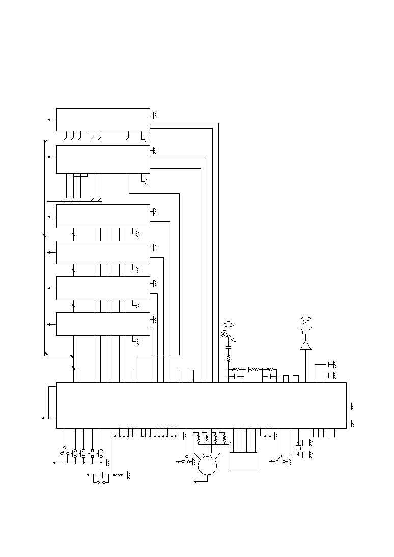
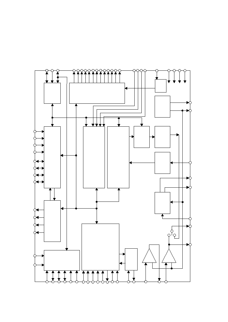
BLOCK DIAGRAM (for MSM6789A (5 V Version))
TEST
TEST
NAR
VPM
RPM
BUSY
CE
XT
XT
MIN
MOUT
LIN
OSC
≠
+
≠
+
LOUT
AMON
FIN
AOUT
FOUT
ADIN
SG
SGC
DROM
DI/O
Data
I/O
Memory Controller
SBC
Analyzer/Synthesizer
LPF
12-bit
ADC
12-bit
DAC
SG
Circuit
DV
DD
AV
DD
DGND
AGND
Test
Circuit
Microcontroller I/F
Status
Register
CE
RD
WR
D0
D1
D2
D3
Address Controller
RSEL1
RSEL2
Timing
Controller
TST
TCK
MCUM
RESET
PDWN
MON
ACON
EXTD
TMD4
TDT4 to TDT7
TMD0 to TMD3
SYNC
MSEL2
MSEL1
WE CS1 CS2 CS3 CS4
A0(SADY)
A1(SADX)
A3(
SAS
)
A4(
RWCK
)
A2(
TAS
)
RAS
A5 to A10
CAS0
to
CAS7
PCM
Synthesizer
LOWPWR
OSC
(RC)
TDT0 to TDT3
[DQ1] to [DQ4]
DRAM/
SR
4B/
1B
° Semiconductor
MSM6789A/6789L
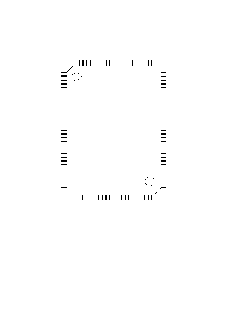
PIN CONFIGURATION (TOP VIEW) (for MSM6789A (5 V Version))
100-Pin Plastic QFP
( ) :
Pins for connecting serial voice ROM.
[ ] :
Pins for connecting 4-bit • type DRAM.
NC :
No-connection pin
1
2
3
4
5
6
7
8
9
10
11
12
13
14
15
16
17
18
19
20
21
22
23
24
25
26
27
28
29
30
80
79
78
77
76
75
74
73
72
71
70
69
68
67
66
65
64
63
62
61
60
59
58
57
56
55
54
53
52
51
LOUT
SGC
SG
AV
DD
AMON
FIN
AOUT
FOUT
ADIN
DGND
TEST
TEST
EXTD
TEST
CE
MCUM
ACON
VPM
TEST
A10
A9
A8
A7
A6
A5
TMD4
TMD3
TMD2
TMD1
TMD0
TDT7
TDT6
TDT5
TDT4
TDT3
TDT2
TDT1
TDT0
SYNC
TST
TCK
D0
D1
D2
D3
BUSY
RPM
A0 (SADY)
A1 (SADX)
A2 (TAS)
A3 (SAS)
A4 (RWCK)
WE
DI/O
MON
NAR
TEST
TEST
TEST
DRAM/SR
CE
RD
WR
TEST
PDWN
RESET
TEST
MSEL2
MSEL1
RSEL2
RSEL1
DGND
AGND
MIN
MOUT
LIN
[DQ4]
[DQ3]
[DQ2]
[DQ1]
100
99
98
97
96
95
94
93
92
91
90
89
88
87
86
85
84
83
82
81
CS1
CS2
CS3
CS4
DROM
RAS
DV
DD
XT
XT
CAS0
CAS1
CAS2
CAS3
CAS4
CAS5
CAS6
CAS7
4B/
1B
31
32
33
34
35
36
37
38
39
40
41
42
43
44
45
46
47
48
49
50
LOWPWR
NC
NC
NC
NC
MSM6789A/6789L
° Semiconductor
PIN DESCRIPTIONS (for MSM6789A (5 V Version))
Symbol
Type
Description
DV
DD
--
Digital power supply. Insert a bypass capacitor of 0.1
mF or more between this
pin and the DGND pin.
AV
DD
--
Analog power supply. Insert a bypass capacitor of 0.1
mF or more between this
pin and the AGND pin.
DGND
--
Digital ground.
AGND
--
Analog ground.
SG, SGC
O
Output for analog circuit reference voltage (signal ground).
MIN
Inverting input of the built-in OP amplifier. The non-inverting input pin is
internally connected to SG (signal ground).
LIN
I
MOUT
Output of the built-in OP amplifier for MIN and LIN.
LOUT
O
AMON
O
Connected to the LOUT pin in the recording mode and to the DA converter
output in the playback mode. This pin connects the built-in LPF input (FIN pin).
FIN
I
FOUT
O
Output of the built-in LPF. This pin connects the AD converter input (ADIN pin).
ADIN
I
Input of the built-in 12-bit AD converter.
AOUT
O
Output of the built-in LPF. This pin outputs playback waveforms and connects
an external speaker drive amplifier.
This pin selects whether memory to be connected externally is DRAM or serial
register.
DRAM/SR
I
Low level
High level
This pin selects either 1-bit
• type DRAM or 4-bit • type DRAM.
4B/1B
I
A0 (SADY)
These pins connect to A0 and A1 of DRAM at the time of DRAM selection. They also
connect to SAD pin of serial register and serial voice ROM at the time of serial
register selection. These pins output leading addresses of read/write.
A1 (SADX)
O
This pin connects to A2 of DRAM at the time of DRAM selection. It also connects
to TAS pin of serial register and serial voice ROM at the time of serial register selection.
This pin is used to set serial addresses from the SADX and SADY pins into the
internal address counter of the serial register and serial voice ROM.
A2 (TAS)
O
This pin connects to A3 of DRAM at the time of DRAM selection. It also connects
to the SAS pin of the serial register and the SASX and SASY pins of the serial voice
ROM at the time of serial register selection. Clock pin to write serial addresses.
A3 (SAS)
O
This pin connects to A4 of DRAM at the time of DRAM selection. It also connects
to the RWCK pin of the serial register and the RDCK pin of the serial voice ROM at
the time of serial register selection. Clock pin to read data from and write data into
the serial register.
A4 (RWCK)
O
Input of the built-in LPF.
: Serial register
: DRAM
Low level
High level
: 1-bit
• type
: 4-bit
• type
A10-A5
O
These pins connect to pins A5-A10 of DRAM at the time of DRAM selection.
These pins output addresses of read/write.
Pin
90
47
40, 55
54
48, 49
53
52
50
46
45
43
42
44
66
88
79
78
77
76
75
1-6
51
° Semiconductor
MSM6789A/6789L
Symbol
Type
Description
WE
O
Write Enable. This pin connects to the WE pin of the serial register and DRAM.
This pin selects either read or write mode.
DI/O
I/O
Data I/O. This pin connects to the DIN and DOUT pins of the serial register and
DRAM. This pin is used to output write data and inputs read data.
DROM
I
Data ROM. This pin connects to the DOUT pin of the serial voice ROM.
RAS
O
This is a row address strobe pin of DRAM at the time of DRAM selection.
CAS0-
CAS7
O
These are the column address strobe pins of DRAM at the time of DRAM selection.
CAS7, an addresss output pin, is connected to pin A11 of DRAM at the time of 16-
Mbit DRAM selection.
CS1
Chip Slect. These pins connect CS pin of the serial register and the CS (CS1,
CS2, CS3) pins of the serial voice ROM.
CS3
O
CS4
MSEL1
I
These pins select the capacity of the memory to be connected externally.
These pins select the number of DRAMs and serial registers to be connected
externallly.
RSEL1
I
CS2
MSEL2
I
RSEL2
I
MSEL2
MSEL1
RSEL2
RSEL1
Memory capacity
L
L
L
L
1M
• 4
L
L
L
H
4M
• 1
L
L
H
L
1M
• 8
L
L
H
H
1M
• 4 + 4M • 1
L
H
L
L
4M
• 2
L
H
L
H
4M
• 2
L
H
H
L
4M
• 3
L
H
H
H
4M
• 3
H
L
L
L
4M
• 4
H
L
L
H
16M
• 1
H
L
H
L
4M
• 6
H
L
H
H
4M
• 6
H
H
L
L
4M
• 8
H
H
L
H
4M
• 8
H
H
H
L
16M
• 2
H
H
H
H
16M
• 2
∑ When DRAM is selected (DRAM/SR = High level)
Pin
74
73
85
89
93-100
81
58
56
59
57
82
83
84
PIN DESCRIPTIONS (for MSM6789A (5 V Version)) (Continued)
MSM6789A/6789L
° Semiconductor
PIN DESCRIPTIONS (for MSM6789A (5 V Version)) (Continued)
Symbol
Type
Description
Mode Selection.
Low level : Stand-alone mode
High level : Microcontroller interface mode
PDWN
I
Power Down. When a low level is input the MSM6789A goes to the power down
state. Unlike the RESET pin, this pin does not force the MSM6789A to be reset.
When an Low level is applied to this pin during recording operation, the MSM6789A
is halted, and will be maintained in the power down state while PDWN is low level.
After this pin is restored to a high level, postprocessing for recording will be
performed.
RSEL1
I
RSEL2
I
MSEL2
MSEL1
RSEL2
RSEL1
Memory capacity
L
L
L
L
4M
• 1
L
L
L
H
4M
• 2
L
L
H
L
4M
• 3
L
L
H
H
4M
• 4
L
H
L
L
8M
• 1
L
H
L
H
8M
• 2
L
H
H
L
8M
• 3
L
H
H
H
8M
• 4
∑ When serial register is selected (DRAM/SR = Low level)
MCUM
I
This pin selects CAS-before-RAS refresh period of DRAM at the time of
power down when DRAM is selected.
Low level : 15 µs max.
High level : 125 µs max.
LOWPWR
I
A high input level causes the MSM6789A to be initialized and to go into the power
down state.
RESET
I
Bidirectional data bus to transfer commands and data to and from an external
microcontroller.
D0
I/O
D1
D2
D3
Write Pulse Input. Inputting a low pulse to WR pin causes a command or data
to be input via D0 to D3 pins.
WR
I
Read Pulse Input. Inputting a low pulse to RD pin causes status bits or data to
be output via D0 to D3 pins.
RD
I
Chip Enable Input. When the CE pin is set to low level and the CE pin is set to a
high level, the write pulse (WR) or read pulse (RD) can be accepted.
When the CE pin is set to a high level or CE pin is set to a low level, the write pulse
(WR) and read pulse (RD) cannot be accepted so that data cannot be communicated
via D0 to D3 pins.
CE
CE
I
Pin
60
56
57
34
87
62
24
25
26
27
63
64
65
35
° Semiconductor
MSM6789A/6789L
PIN DESCRIPTIONS (for MSM6789A (5 V Version)) (Continued)
Symbol
Type
Description
Oscillator Connect. When an external clock is used, input the clock through
this pin. At the power-down state, this pin must be set to the ground level.
XT
I
TEST
MSM6789A Test. Input a low level to the TEST pin and a high level to the
TEST pin.
TEST
I
Oscillator Connect. When an external clock is uesd, this pin must be left open.
XT
O
MSM6789A Test. This pin must be left open.
TMD3-TMD0
TDT7-TDT0
SYNC
I/O
Connect these pins to DQ1 to DQ4 of DRAM at the time of 4-bit
• type DRAM
selection. Otherwise these pins must be left open as they are MSM6789A test pins.
TDT3-TDT0
[DQ4]-[DQ1]
I/O
MSM6789A Test. Input a low level.
TST
TCK
TMD4
I
RPM. This pin outputs a high level during recording or playback operation. The
state of this pin is the same as the contents of the RPM bit of the status register.
RPM
O
VPM. This pin outputs a high level during standby for voice incoming after the start of
recording by voice triggered starting or unvoiced-part elimination. Also outputs a high
level when the record/playback is stopped temporarily by inputting the PAUSE
command. The state of this pin is the same as the contents of the VPM bit of the
status register.
VPM
O
NAR. This NAR pin indicates whether the phrase designation by the CHAN command
is enabled or disabled.
In the ROM play back operation, specify the next phrase after verifying that the NAR
pin is at high level and input the START command.
NAR
O
P
OP
Noise Suppression Select. This pin selects whether the pop noise
suppression circuit is used.
Low level : the pop noise suppression circuit is not used.
High level : the pop noise suppression circuit is used.
The DC level is shifted by the LEV command.
ACON
I
EXTD. In the record/playback operation by the EXT command, input a high level for
read/write of SBC data. Input a low level for usual command input and status output.
EXTD
I
MON. This pin outputs a high level while the record/playback operation is being
performed. Outputs a synchronizing clock while record/playback activated by the
EXT command is being performed.
MON
O
Busy. This pin outputs a high level while a command is being executed. When this
pin is held high, do not apply any data to D0 to D3 pins. The state of this pin is the
same as the contents of the BUSY bit of the status register.
BUSY
O
Pin
91
36, 37-39,
61, 67-70
33
92
9-12
13-20
21
17-20
22
23
8
30
31
71
32
37
72
29
MSM6789A/6789L
° Semiconductor
ABSOLUTE MAXIMUM RATINGS (for MSM6789A (5 V Version))
Parameter
Symbol
Rating
Condition
Unit
Power supply voltage
V
DD
≠0.3 to +7.0
Ta=25∞C
V
Input Voltage
V
IN
≠0.3 ~ V
DD
+0.3
Ta=25∞C
V
Storage temperature
T
STG
≠55 to +150
--
∞C
RECOMMENDED OPERATING CONDITIONS (for MSM6789A (5 V Version))
ELECTRIAL CHARACTERISTICS (for MSM6789A (5 V Version))
DC Characteristics
*1 Applies to all inputs excluding the XT pin.
*2 Applies to the XT pin.
*3 The record/playback operation must be performed at the power supply voltage of 4.5 to 5.5 V.
The MSM6789A operates at 3.5 to 5.5 V when the serial register is backed up.
Parameter
Symbol
Condition
High input voltage
V
IH
--
Low input voltage
V
IL
--
Min.
0.8
•V
DD
--
Typ.
--
--
Unit
V
V
Max.
--
0.2
•V
DD
High output voltage
V
OH
I
OH
=≠40
mA
V
DD
≠0.3
--
V
--
Low output voltage
V
OL
I
OL
=2 mA
--
--
V
0.45
High input current
*1
I
IH1
V
IH
=V
DD
--
--
mA
10
High input current
*2
I
IH2
V
IH
=V
DD
--
--
mA
20
Low input current
*1
I
IL1
V
IL
=GND
≠10
--
mA
--
Low input current
*2
I
IL2
V
IL
=GND
≠20
--
mA
--
Operating current consumption
I
DD
f
OSC
=8 MHz, no load
--
20
mA
35
Power down current
No load
Serial register connected
I
DDS1
--
--
mA
10
--
200
mA
--
I
DDS2
No load
DRAM connected
DV
DD
=AV
DD
=4.5 to 5.5 V
*3
DGND=AGND=0 V Ta=0 to 70∞C
Parameter
Symbol
Range
Condition
Unit
Power supply voltage
V
DD
+3.5 to +5.5
*3
DGND=AGND=0 V
V
Operating temperature
T
op
0 to +70
--
∞C
Master clock frequencuy
f
OSC
6.0 to 8.192
--
MHz
° Semiconductor
MSM6789A/6789L
Parameter
Symbol
Condition
DA output relative error
V
DAE
No load
FIN admissible input voltage range
V
FIN
--
Min.
--
1
Typ.
--
--
Unit
mV
V
Max.
10
V
DD
≠1
FIN input impedance
R
FIN
1
--
M
W
--
OP-amp open loop gain
G
OP
40
--
dB
---
OP-amp input impedance
R
INA
1
--
M
W
--
OP-amp load resistance
R
OUTA
200
--
k
W
--
AOUT load resistance
R
AOUT
50
--
k
W
--
FOUT load resistance
R
FOUT
50
--
k
W
--
--
f
IN
=0 to 4 kHz
--
--
--
--
DV
DD
=AV
DD
=4.5 to 5.5 V
DGND=AGND=0 V Ta=0 to 70∞C
Analog Characteristics
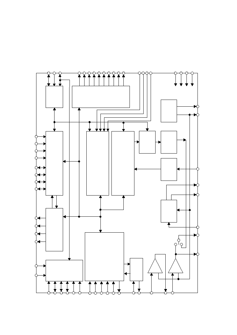
MSM6789A/6789L
° Semiconductor
BLOCK DIAGRAM (for MSM6789L (3.3 V Version))
TEST
TEST
NAR
VPM
RPM
BUSY
CE
XT
XT
MIN
MOUT
LIN
OSC
≠
+
≠
+
LOUT
AMON
FIN
AOUT
FOUT
ADIN
SG
SGC
DROM
DI/O
Data
I/O
Memory Controller
SBC
Analyzer/Synthesizer
LPF
12-bit
ADC
12-bit
DAC
SG
Circuit
DV
DD
AV
DD
DGND
AGND
Test
Circuit
Microcontroller I/F
Status
Register
CE
RD
WR
D0
D1
D2
D3
Address Controller
RSEL1
RSEL2
Timing
Controller
TST
TCK
MCUM
RESET
PDWN
MON
ACON
EXTD
TMD4
TDT4 to TDT7
TMD0 to TMD3
SYNC
MSEL2
MSEL1
WE
CS1
CS2
CS3
CS4
SADY
SADX
SAS
RWCK
TAS
PCM
Synthesizer
TDT0 to TDT3
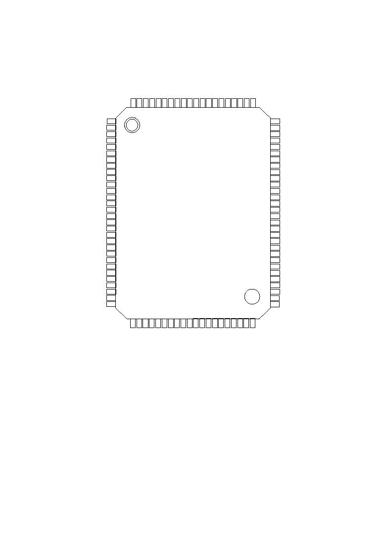
° Semiconductor
MSM6789A/6789L
PIN CONFIGURATION (TOP VIEW) (for MSM6789L (3.3V Version))
100-Pin Plastic QFP
NC :
No-connection pin
1
2
3
4
5
6
7
8
9
10
11
12
13
14
15
16
17
18
19
20
21
22
23
24
25
26
27
28
29
30
80
79
78
77
76
75
74
73
72
71
70
69
68
67
66
65
64
63
62
61
60
59
58
57
56
55
54
53
52
51
LOUT
SGC
SG
AV
DD
AMON
FIN
AOUT
FOUT
ADIN
DGND
TEST
TEST
EXTD
TEST
CE
MCUM
ACON
VPM
TEST
TMD4
TMD3
TMD2
TMD1
TMD0
TDT7
TDT6
TDT5
TDT4
TDT3
TDT2
TDT1
TDT0
SYNC
TST
TCK
D0
D1
D2
D3
BUSY
RPM
SADY
SADX
TAS
SAS
RWCK
WE
DI/O
MON
NAR
TEST
TEST
TEST
TEST
CE
RD
WR
TEST
PDWN
RESET
TEST
MSEL2
MSEL1
RSEL2
RSEL1
DGND
AGND
MIN
MOUT
LIN
100
99
98
97
96
95
94
93
92
91
90
89
88
87
86
85
84
83
82
81
CS1
CS2
CS3
CS4
DROM
DV
DD
XT
XT
TEST
31
32
33
34
35
36
37
38
39
40
41
42
43
44
45
46
47
48
49
50
TEST
NC
NC
NC
NC
NC
NC
NC
NC
NC
NC
NC
NC
NC
NC
NC
NC
NC
NC
NC
NC
MSM6789A/6789L
° Semiconductor
PIN DESCRIPTIONS (for MSM6789L (3.3 V Version))
Symbol
Type
Description
DV
DD
--
Digital power supply. Insert a bypass capacitor of 0.1
mF or more between this
pin and the DGND pin.
AV
DD
--
Analog power supply. Insert a bypass capacitor of 0.1
mF or more between this
pin and the AGND pin.
DGND
--
Digital ground.
AGND
--
Analog ground.
SG, SGC
O
Output for analog circuit reference voltage (signal ground).
MIN
Inverting input of the built-in OP amplifier. The non-inverting input pin is
internally connected to SG (signal ground).
LIN
I
MOUT
Output of the built-in OP amplifier for MIN and LIN.
LOUT
O
AMON
O
Connected to the LOUT pin in the recording mode and to the DA converter
output in the playback mode. This pin connects the built-in LPF input (FIN pin).
FIN
I
FOUT
O
Output of the built-in LPF. This pin connects the AD converter input (ADIN pin).
ADIN
I
Input of the built-in 12-bit AD converter.
AOUT
O
Output of the built-in LPF. This pin outputs playback waveforms and connects
an external speaker drive amplifier.
SADY
These pins connect to SAD pin of serial register and serial voice ROM. These pins
output leading addresses of read/write.
SADX
O
This pin connects to TAS pin of serial register and serial voice ROM. This pin is used
to set serial addresses from the SADX and SADY pins into the internal address
counter of the serial register and serial voice ROM.
TAS
O
This pin connects to the SAS pin of the serial register and the SASX and SASY pins
of the serial voice ROM. Clock pin to write serial addresses.
SAS
O
This pin connects to the RWCK pin of the serial register and the RDCK pin of the
serial voice ROM. Clock pin to read data from and write data into the serial register.
RWCK
O
Input of the built-in LPF.
Pin
90
47
40, 55
54
48, 49
53
52
50
46
45
43
42
44
79
78
77
76
75
51
WE
O
Write Enable. This pin connects to the WE pin of the serial register and DRAM.
This pin selects either read or write mode.
DI/O
I/O
Data I/O. This pin connects to the DIN and DOUT pins of the serial register and
DRAM. This pin is used to output write data and inputs read data.
DROM
I
Data ROM. This pin connects to the DOUT pin of the serial voice ROM.
CS1
Chip Slect. These pins connect CS pin of the serial register and the CS (CS1,
CS2, CS3) pins of the serial voice ROM.
CS3
O
CS4
MSEL1
I
These pins select the capacity of the memory to be connected externally.
CS2
MSEL2
I
74
73
85
81
58
59
82
83
84
° Semiconductor
MSM6789A/6789L
PIN DESCRIPTIONS (for MSM6789L (3.3 V Version)) (Continued)
Symbol
Type
Description
Mode Selection.
Low level : Stand-alone mode
High level : Microcontroller interface mode
PDWN
I
Power Down. When a low level is input the MSM6789L goes to the power down
state. Unlike the RESET pin, this pin does not force the MSM6789L to be reset.
When an Low level is applied to this pin during recording operation, the MSM6789L
is halted, and will be maintained in the power down state while PDWN is low level.
After this pin is restored to a high level, postprocessing for recording will be
performed.
RSEL1
I
RSEL2
I
MSEL2
MSEL1
RSEL2
RSEL1
Memory capacity
L
L
L
L
4M
• 1
L
L
L
H
4M
• 2
L
L
H
L
4M
• 3
L
L
H
H
4M
• 4
These pins select the number of serial registers to be connected
externallly.
MCUM
I
A high input level causes the MSM6789L to be initialized and to go into the power
down state.
RESET
I
Bidirectional data bus to transfer commands and data to and from an external
microcontroller.
D0
I/O
D1
D2
D3
Write Pulse Input. Inputting a low pulse to WR pin causes a command or data
to be input via D0 to D3 pins.
WR
I
Read Pulse Input. Inputting a low pulse to RD pin causes status bits or data to
be output via D0 to D3 pins.
RD
I
Chip Enable Input. When the CE pin is set to low level and the CE pin is set to a
high level, the write pulse (WR) or read pulse (RD) can be accepted.
When the CE pin is set to a high level or CE pin is set to a low level, the write pulse
(WR) and read pulse (RD) cannot be accepted so that data cannot be communicated
via D0 to D3 pins.
CE
CE
I
Pin
60
56
57
34
62
24
25
26
27
63
64
65
35
RPM. This pin outputs a high level during recording or playback operation. The
state of this pin is the same as the contents of the RPM bit of the status register.
RPM
O
Busy. This pin outputs a high level while a command is being executed. When this
pin is held high, do not apply any data to D0 to D3 pins. The state of this pin is the
same as the contents of the BUSY bit of the status register.
BUSY
O
30
29
MSM6789A/6789L
° Semiconductor
PIN DESCRIPTIONS (for MSM6789L (3.3 V Version)) (Continued)
Symbol
Type
Description
Oscillator Connect. When an external clock is used, input the clock through
this pin. At the power-down state, this pin must be set to the ground level.
XT
I
TEST
MSM6789L Test. Input a low level to the TEST pin and a high level to the
TEST pin.
TEST
I
Oscillator Connect. When an external clock is uesd, this pin must be left open.
XT
O
MSM6789L Test. This pin must be left open.
TMD3-TMD0
TDT7-TDT0
SYNC
I/O
These pins must be left open as they are MSM6789L test pins.
TDT3-TDT0
I/O
MSM6789L Test. Input a low level.
TST
TCK
TMD4
I
VPM. This pin outputs a high level during standby for voice incoming after the start of
recording by voice triggered starting or unvoiced-part elimination. Also outputs a high
level when the record/playback is stopped temporarily by inputting the PAUSE
command. The state of this pin is the same as the contents of the VPM bit of the
status register.
VPM
O
NAR. This NAR pin indicates whether the phrase designation by the CHAN command
is enabled or disabled.
In the ROM play back operation, specify the next phrase after verifying that the NAR
pin is at high level and input the START command.
NAR
O
P
OP
Noise Suppression Select. This pin selects whether the pop noise
suppression circuit is used.
Low level : the pop noise suppression circuit is not used.
High level : the pop noise suppression circuit is used.
The DC level is shifted by the LEV command.
ACON
I
EXTD. In the record/playback operation by the EXT command, input a high level for
read/write of SBC data. Input a low level for usual command input and status output.
EXTD
I
MON. This pin outputs a high level while the record/playback operation is being
performed. Outputs a synchronizing clock while record/playback activated by the
EXT command is being performed.
MON
O
Pin
91
36, 37-39,
61, 67-70
33
92
9-12
13-20
21
17-20
22
23
8
31
71
32
37
72
° Semiconductor
MSM6789A/6789L
ABSOLUTE MAXIMUM RATINGS (for MSM6789L (3.3 V Version))
RECOMMENDED OPERATING CONDITIONS (for MSM6789L (3.3 V Version))
ELECTRIAL CHARACTERISTICS (for MSM6789L (3.3 V Version))
DC Characteristics
*1 Applies to all inputs excluding the XT pin.
*2 Applies to the XT pin.
Parameter
Symbol
Rating
Condition
Unit
Power supply voltage
V
DD
≠0.3 to +7.0
Ta=25∞C
V
Input Voltage
V
IN
≠0.3 ~ V
DD
+0.3
Ta=25∞C
V
Storage temperature
T
STG
≠55 to +150
--
∞C
Parameter
Symbol
Range
Condition
Unit
Power supply voltage
V
DD
+3.0 to +3.6
DGND=AGND=0 V
V
Operating temperature
T
op
0 to +70
--
∞C
Master clock frequencuy
f
OSC
6.0 to 8.192
--
MHz
Parameter
Symbol
Condition
High input voltage
V
IH
--
Low input voltage
V
IL
--
Min.
0.85
•V
DD
--
Typ.
--
--
Unit
V
V
Max.
--
0.15
•V
DD
High output voltage
V
OH
I
OH
=≠40
mA
V
DD
≠0.3
--
V
--
Low output voltage
V
OL
I
OL
=2 mA
--
--
V
0.45
High input current
*1
I
IH1
V
IH
=V
DD
--
--
mA
10
High input current
*2
I
IH2
V
IH
=V
DD
--
--
mA
20
Low input current
*1
I
IL1
V
IL
=GND
≠10
--
mA
--
Low input current
*2
I
IL2
V
IL
=GND
≠20
--
mA
--
Operating current consumption
I
DD
f
OSC
=8 MHz, no load
--
20
mA
35
Power down current
No load
Serial register connected
I
DDS1
--
--
mA
10
--
200
mA
--
I
DDS2
No load
DRAM connected
DV
DD
=AV
DD
=3.0 to 3.6 V
DGND=AGND=0 V Ta=0 to 70∞C

MSM6789A/6789L
° Semiconductor
Parameter
Symbol
Condition
DA output relative error
V
DAE
No load
FIN admissible input voltage range
V
FIN
--
Min.
--
1
Typ.
--
--
Unit
mV
V
Max.
20
V
DD
≠1
FIN input impedance
R
FIN
1
--
M
W
--
OP-amp open loop gain
G
OP
40
--
dB
---
OP-amp input impedance
R
INA
1
--
M
W
--
OP-amp load resistance
R
OUTA
400
--
k
W
--
AOUT load resistance
R
AOUT
100
--
k
W
--
FOUT load resistance
R
FOUT
100
--
k
W
--
--
f
IN
=0 to 4 kHz
--
--
--
--
DV
DD
=AV
DD
=3.0 to 3.6 V
DGND=AGND=0 V Ta=0 to 70∞C
Analog Characteristics
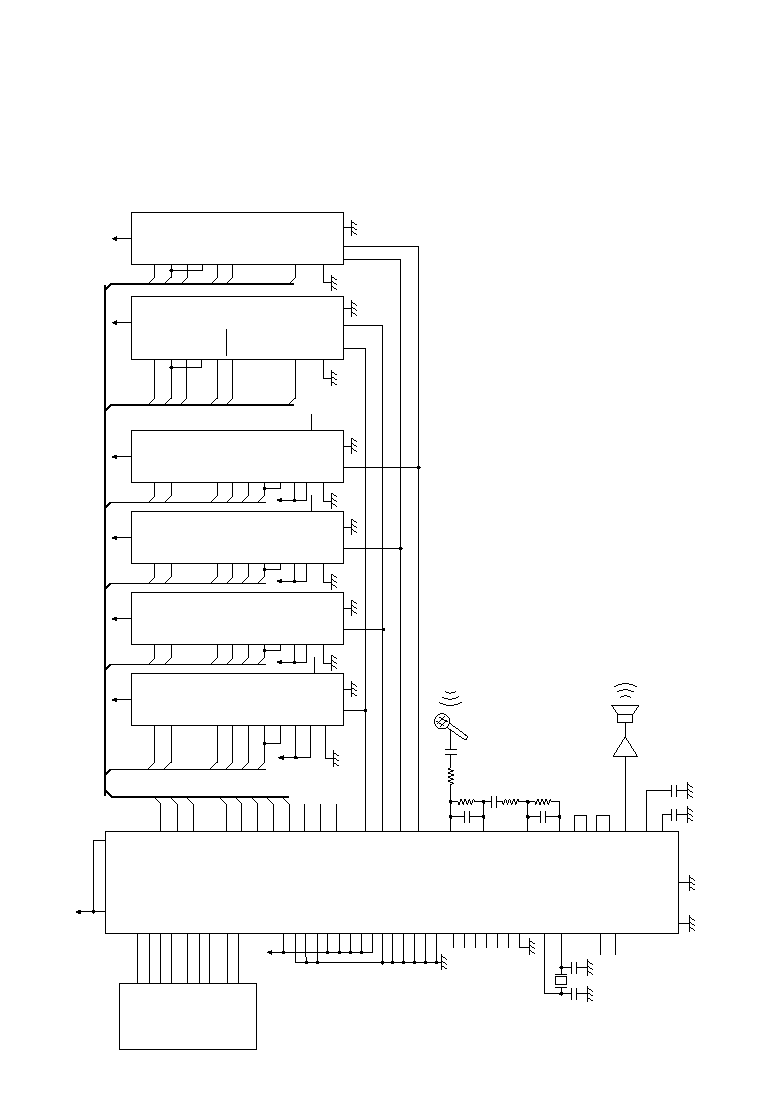
° Semiconductor
MSM6789A/6789L
APPLICATION CIRCUITS (for MSM6789A (5 V Version))
This is an application circuit example when the MSM6789A is used in microcontroller interface mode
with four 8-Mbit serial registers and two 2-Mbit serial voice ROMs.
+
DGND
+
D3
MCUM
RSEL1
RSEL2
CE TEST
BUSY
RPM
VPM
XT
XT
MON
NAR
AGND
SG
SGC
AOUT
ADIN
FOUT
FIN
AMON
LOUT
LIN
MOUT
MIN
CS4
CS3
CS2
CS1
DROM
DI/O
WE
RWCK
TAS
SADY
SAS
SADX
AV
DD
DV
DD
Speaker drive amplifier
RECORDER IC MSM6789A
D2
D1
D0
RD WR CE
RESET
PDWN
Microcontroller
SYNC
TDT0-7
TMD0-3
TMD4
SADX
SAD
SAS
SAS
TAS
TAS
RWCK
RWCK
WE
WE
DI/O
DIN
DOUT
TEST
RS/A
CS
V
SS
V
CC
SADX
SADX
SAS
SASX
TAS
TAS
RWCK
RDCK
DOUT
TEST
CS1
CS2
V
CC
SADY
SADY
SASY
DROM
V
SS
8.192 MHz
8M Serial Register MSM6685
MSM6685
MSM6685
MSM6685
2M Serial Voice ROM
MSM6596A-XXX
MSM6596A-XXX
RFSH
NC
LOWPWR
DRAM/
SR
MSEL2
MSEL1
TST
TCK
TEST
EXTD
ACON
4B/
1B
CAS0
-
CAS7
RAS
A5-A10
Circuit
1
:
Application circuit in microcontroller interface mode with 8-Mbit
serial registers and 2-Mbit serial voice ROMs.
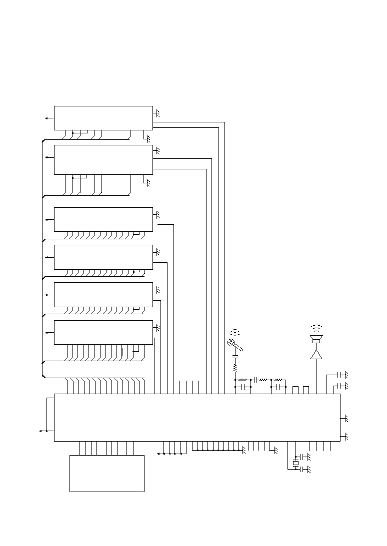
MSM6789A/6789L
° Semiconductor
APPLICATION CIRCUITS (for MSM6789A (5 V Version)) (Continued)
This is an application circuit example when the MSM6789A is used in microcontroller interface mode
with four 4-Mbit DRAMs (1-bit • type) and two 2-Mbit serial voice ROMs.
DGND
D3
RESET
RD
WR
MCUM
XT
XT
MON
NAR
AGND
SG
SGC
AOUT
ADIN
FOUT
FIN
AMON
LOUT
LIN
MOUT
MIN
CS4
CS3
CS2
CS1
CAS4
DI/O
WE
A4(
RWCK
)
A2(
TAS
)
A0(SADY)
A3(
SAS
)
A1(SADX)
AV
DD
DV
DD
CAS
V
SS
V
CC
SADX
SADX
SAS
SASX
TAS
TAS
RWCK
RDCK
DOUT
TEST
CS1
CS2
V
CC
SADY
SADY
SASY
DROM
V
SS
RECORDER IC MSM6789A
4-Mbit DRAM MSM514100A
2M Serial Voice ROM
MSM6596A-XXX
MSM6596A-XXX
TDT0-7
TMD0-3
TMD4
CE
8.192 MHz
+
+
Speaker drive amplifier
CAS5
CAS6
CAS7
DROM
CAS0
CAS1
CAS2
CAS3
A5
A6
A7
RAS
A8
A9
A10
DIN
WE
A4
A2
A0
A1
DOUT
A5
A6
A7
RAS
A8
A9
A10
A3
DI/O
WE
A4
A2
A0
A1
A5
A6
A7
A8
A9
A10
A3
MSM514100A
MSM514100A
MSM514100A
V
CC
V
CC
V
CC
CAS
V
SS
CAS
V
SS
CAS
V
SS
D2
D1
D0
CE
PDWN
TEST
SYNC
VPM
RPM
BUSY
Microcontroller
MSEL1
TEST
EXTD
TCK
TST
ACON
RSEL2
RSEL1
LOWPWR
MSEL2
DRAM/
SR
4B/
1B
Circuit
2
:
Application circuit in microcontroller interface mode with 4-Mbit
DRAMs and 2-Mbit serial voice ROMs.
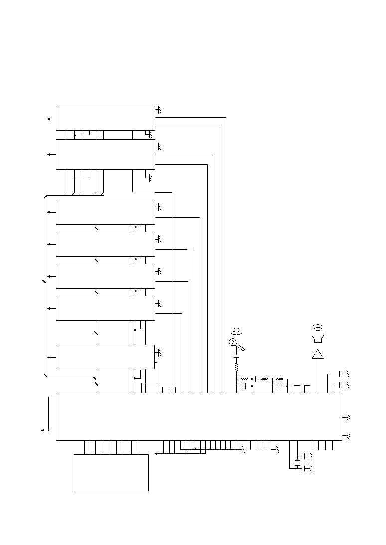
° Semiconductor
MSM6789A/6789L
APPLICATION CIRCUITS (for MSM6789A (5 V Version)) (Continued)
This is an application circuit example when the MSM6789A is used in microcontroller interface mode
with one 4-Mbit DRAM, four 1-Mbit DRAMs (1-bit • type), and two 2-Mbit serial voice ROMs.
DGND
AGND
SG
SGC
AOUT
ADIN
FOUT
FIN
AMON
LOUT
LIN
MOUT
MIN
CS4
CS3
CS2
CS1
CAS4
DI/O
WE
AV
DD
DV
DD
V
CC
A1(SADX)
SADX
A3(
SAS
)
SASX
A2(
TAS
)
TAS
A4(
RWCK
)
RDCK
DOUT
TEST
CS1
CS2
V
CC
A0(SADY)
SADY
SASY
DROM
V
SS
RECORDER IC MSM6789A
1-Mbit DRAM MSM511000A
2M Serial Voice ROM
MSM6596A-XXX
MSM6596A-XXX
+
+
Speaker drive amplifier
CAS5
CAS6
CAS7
DROM
CAS0
CAS1
CAS2
CAS3
RAS
A0-A9
MSM511000A
MSM511000A
MSM511000A
A0-A10
V
CC
CAS
V
SS
WE DIN
DOUT
RAS
A0-A4
A0-A10
11
10
10
10
10
5
4-Mbit DRAM MSM514100A
CAS
V
SS
CAS
V
SS
CAS
V
SS
V
CC
V
CC
V
CC
D3
RESET
RD
RSEL2
RSEL1
WR
MCUM
XT
XT
MON
NAR
TDT0-7
TMD0-3
TEST
TMD4
CE
EXTD
TCK
TST
ACON
D2
D1
D0
CE
PDWN
TEST
SYNC
VPM
RPM
BUSY
MSEL2
MSEL1
8.192 MHz
Microcontroller
LOWPWR
DRAM/
SR
4B/
1B
CAS
V
SS
Circuit
3
:
Application circuit in microcontroller interface mode with 4-Mbit
DRAMs, 1-Mbit DRAMs, and 2-Mbit serial voice ROMs.
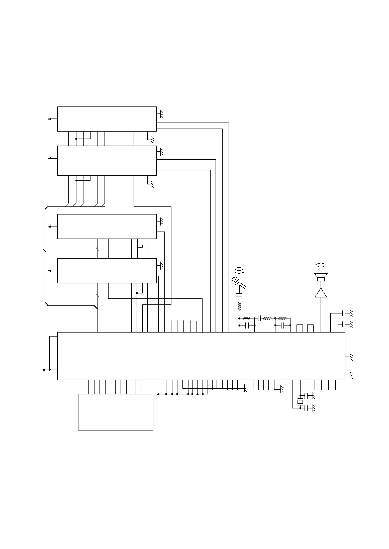
MSM6789A/6789L
° Semiconductor
APPLICATION CIRCUITS (for MSM6789A (5 V Version)) (Continued)
This is an application circuit example when the MSM6789A is used in microcontroller interface mode
with two 16-Mbit DRAMs (1-bit • type) and two 2-Mbit serial voice ROMs.
DGND
AGND
SG
SGC
AOUT
ADIN
FOUT
FIN
AMON
LOUT
LIN
MOUT
MIN
CS4
CS3
CS2
CS1
CAS4
DI/O
WE
AV
DD
DV
DD
CAS
V
SS
V
CC
A1(SADX)
SADX
A3(
SAS
)
SASX
A2(
TAS
)
TAS
A4(
RWCK
)
RDCK
DOUT
TEST
CS1
CS2
V
CC
A0(SADY)
SADY
SASY
DROM
V
SS
RECORDER IC MSM6789A
16-Mbit DRAM MSM5116100A
2M Serial Voice ROM
MSM6596A-XXX
MSM6596A-XXX
+
+
Speaker drive amplifier
CAS5
CAS6
CAS7
DROM
CAS0
CAS1
CAS2
CAS3
RAS
DIN
WE
DOUT
A0-A10
A11
RAS
A0-A10
MSM5116100A
V
CC
CAS
V
SS
11
A0-A10
11
A0-A10
5
A0-A4
8.192 MHz
Microcontroller
D3
RESET
RD
RSEL2
RSEL1
WR
MCUM
XT
XT
MON
NAR
TDT0-7
TMD0-3
TMD4
CE
TEST
EXTD
TCK
TST
ACON
D2
D1
D0
CE
PDWN
TEST
SYNC
VPM
RPM
BUSY
MSEL2
MSEL1
LOWPWR
DRAM/
SR
4B/
1B
Circuit
4
:
Application circuit in microcontroller interface mode
with 16-Mbit DRAMs and 2-Mbit serial voice ROMs.
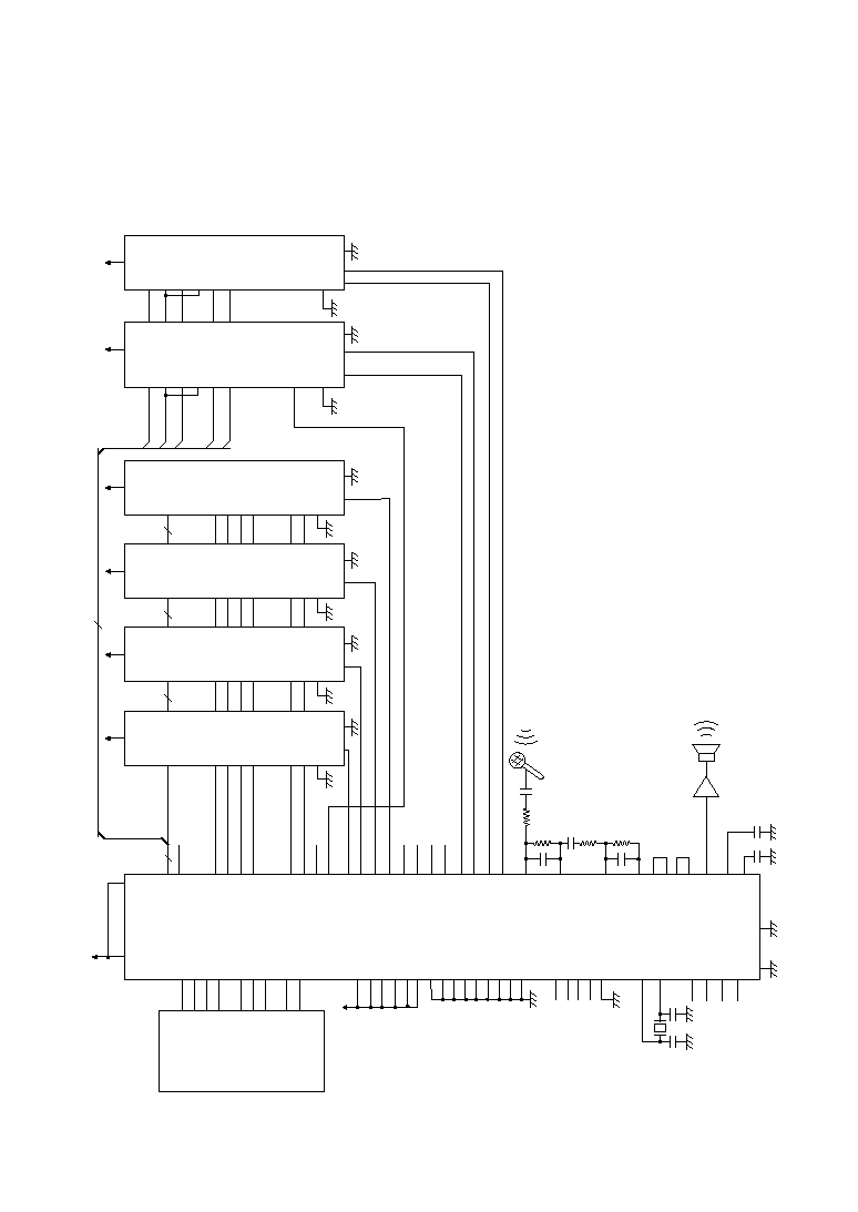
° Semiconductor
MSM6789A/6789L
DGND
D3
RESET
RD
WR
MCUM
XT
XT
MON
NAR
AGND
SG
SGC
AOUT
ADIN
FOUT
FIN
AMON
LOUT
LIN
MOUT
MIN
CS4
CS3
CS2
CS1
CAS4
DI/O
WE
A10
A0-A9
AV
DD
DV
DD
CAS
V
SS
V
CC
A1(SADX)
SADX
A3(
SAS
)
SASX
A2(
TAS
)
TAS
A4(
RWCK
)
RDCK
DOUT
TEST
CS1
CS2
V
CC
A0(SADY)
SADY
SASY
DROM
V
SS
RECORDER IC MSM6789A
4-Mbit DRAM MSM514400C
2M Serial Voice ROM
MSM6596A-XXX
MSM6596A-XXX
TDT4-7
TMD0-3
TMD4
CE
8.192 MHz
+
+
Speaker drive amplifier
CAS5
CAS6
CAS7
DROM
CAS0
CAS1
CAS2
CAS3
[TDT0]DQ1
[TDT1]DQ2
[TDT2]DQ3
RAS
[TDT3]DQ4
WE
DQ1
DQ2
DQ3
RAS
DQ4
MSM514400C
MSM514400C
MSM514400C
V
CC
V
CC
V
CC
CAS
V
SS
CAS
V
SS
CAS
V
SS
D2
D1
D0
CE
PDWN
TEST
SYNC
VPM
RPM
BUSY
Microcontroller
MSEL1
TEST
EXTD
TCK
TST
ACON
RSEL2
RSEL1
LOWPWR
MSEL2
DRAM/
SR
4B/
1B
10
10
10
10
5
OE
APPLICATION CIRCUITS (for MSM6789A (5 V Version)) (Continued)
This is an application circuit example when the MSM6789A is used in microcontroller interface mode
with four 4-Mbit DRAMs (4-bit • type) and two 2-Mbit serial voice ROMs.
Circuit
5
:
Application circuit in microcontroller interface mode with 4-Mbit
DRAMs and 2-Mbit serial voice ROMs.
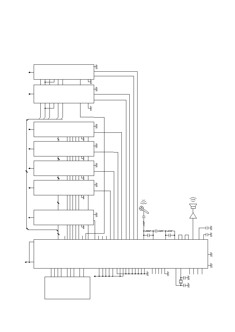
MSM6789A/6789L
° Semiconductor
APPLICATION CIRCUITS (for MSM6789A (5 V Version)) (Continued)
This is an application circuit example when the MSM6789A is used in microcontroller interface mode
with one 4-Mbit DRAM, four 1-Mbit DRAMs (4-bit • type), and two 2-Mbit serial voice ROMs.
DGND
AGND
SG
SGC
AOUT
ADIN
FOUT
FIN
AMON
LOUT
LIN
MOUT
MIN
CS4
CS3
CS2
CS1
CAS4
DI/O
WE
AV
DD
DV
DD
V
CC
A1(SADX)
SADX
A3(
SAS
)
SASX
A2(
TAS
)
TAS
A4(
RWCK
)
RDCK
DOUT
TEST
CS1
CS2
V
CC
A0(SADY)
SADY
SASY
DROM
V
SS
RECORCDER IC MSM6789A
1-Mbit DRAM MSM514256B
2M Serial Voice ROM
MSM6596A-XXX
MSM6596A-XXX
+
+
Speaker drive amplifier
CAS5
CAS6
CAS7
DROM
CAS0
CAS1
CAS2
CAS3
RAS
A0-A8
MSM514256B
MSM514256B
MSM514256B
A0-A9
V
CC
CAS
V
SS
WE
RAS
A0-A4
A0-A9
10
9
99
9
5
4-Mbit DRAM MSM514400C
CAS
V
SS
CAS
V
SS
CAS
V
SS
V
CC
V
CC
V
CC
D3
RESET
RD
RSEL2
RSEL1
WR
MCUM
XT
XT
MON
NAR
TDT4-7
TMD0-3
TEST
TMD4
CE
EXTD
TCK
TST
ACON
D2
D1
D0
CE
PDWN
TEST
SYNC
VPM
RPM
BUSY
MSEL2
MSEL1
8.192 MHz
Microctontroller
LOWPWR
DRAM/
SR
4B/
1B
A10
[TDT0]DQ1 [TDT1]DQ2 [TDT2]DQ3
[TDT3]DQ4
DQ1 DQ2 DQ3
DQ4
CAS
V
SS
OE
Circuit
6
:
Application circuit in microcontroller interface mode with 4-Mbit
DRAM, 1-Mbit DRAMs, and 2-Mbit serial voice ROMs.
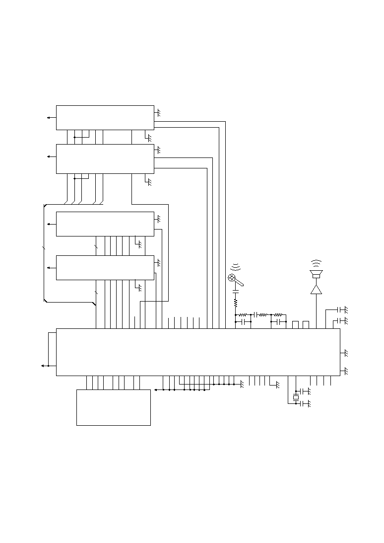
° Semiconductor
MSM6789A/6789L
APPLICATION CIRCUITS (for MSM6789A (5 V Version)) (Continued)
This is an application circuit example when the MSM6789A is used in microcontroller interface mode
with two 16-Mbit DRAMs (4-bit • type) and two 2-Mbit serial voice ROMs.
DGND
AGND
SG
SGC
AOUT
ADIN
FOUT
FIN
AMON
LOUT
LIN
MOUT
MIN
CS4
CS3
CS2
CS1
CAS4
DI/O
WE
AV
DD
DV
DD
CAS
V
SS
V
CC
A1(SADX)
SADX
A3(
SAS
)
SASX
A2(
TAS
)
TAS
A4(
RWCK
)
RDCK
DOUT
TEST
CS1
CS2
V
CC
A0(SADY)
SADY
SASY
DROM
V
SS
RECORDER IC MSM6789A
16-Mbit DRAM MSM5117400A
2M Serial Voice ROM
MSM6596A-XXX
MSM6596A-XXX
+
+
Speaker drive amplifier
CAS5
CAS6
CAS7
DROM
CAS0
CAS1
CAS2
CAS3
RAS
WE
A0~A10
RAS
A0-A10
MSM5117400A
V
CC
CAS
V
SS
11
A0-A10
11
A0-A10
5
A0-A4
8.192 MHz
Microcontroller
D3
RESET
RD
RSEL2
RSEL1
WR
MCUM
XT
XT
MON
NAR
TDT4-7
TMD0-3
TMD4
CE
TEST
EXTD
TCK
TST
ACON
D2
D1
D0
CE
PDWN
TEST
SYNC
VPM
RPM
BUSY
MSEL2
MSEL1
LOWPWR
DRAM/
SR
4B/
1B
[TDT0]DQ1
[TDT1]DQ2
[TDT2]DQ3
[TDT3]DQ4
DQ1
DQ2
DQ3
DQ4
OE
Circuit
7
:
Application circuit in microcontroller interface mode
with 16-Mbit DRAMs and 2-Mbit serial voice ROMs.
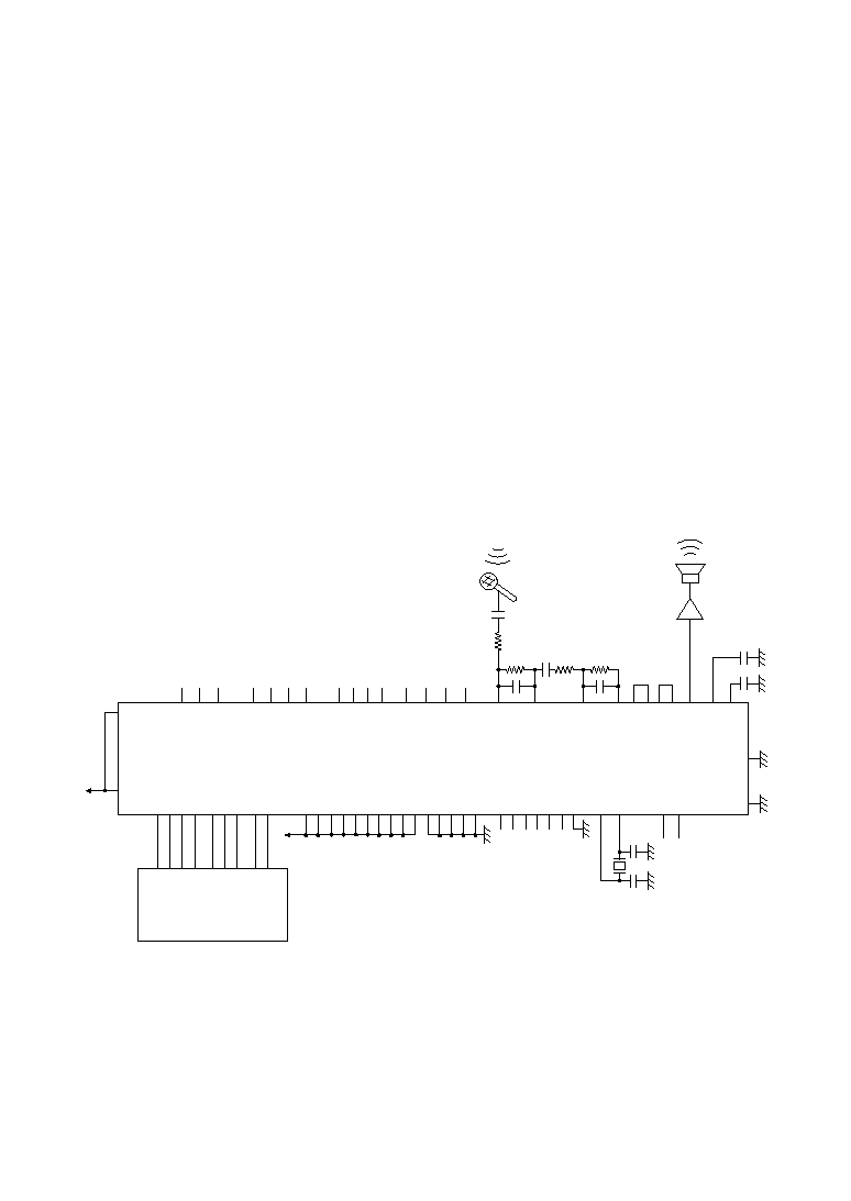
MSM6789A/6789L
° Semiconductor
APPLICATION CIRCUITS (for MSM6789A (5 V Version)) (Continued)
This is an application circuit example when the EXT command is used for recording/playback.
MCUM
+
DGND
+
D3
RSEL1
RSEL2
CE
TEST
ACON
XT
XT
MON
NAR
AGND
SG
SGC
AOUT
ADIN
FOUT
FIN
AMON
LOUT
LIN
MOUT
MIN
CS4
CS3
CS2
CS1
DROM
DI/O
WE
A4(
RWCK
)
A2(
TAS
)
A0(SADY)
A3(
SAS
)
A1(SADX)
AV
DD
DV
DD
Speaker drive amplifier
RECORDER IC MSM6789A
D2
D1
D0
RD WR CE
RESET
EXTD
Microcontroller
TST
TCK
TEST
PDWN
8.192 MHz
BUSY
RPM
VPM
SYNC
TDT0-7
TMD0-3
TMD4
MSEL1
MSEL2
LOWPWR
DRAM/
SR
4B/
1B
RAS
CAS0
-
CAS7
A5-A10
Circuit 8 :
Application circuit when EXT command is used.
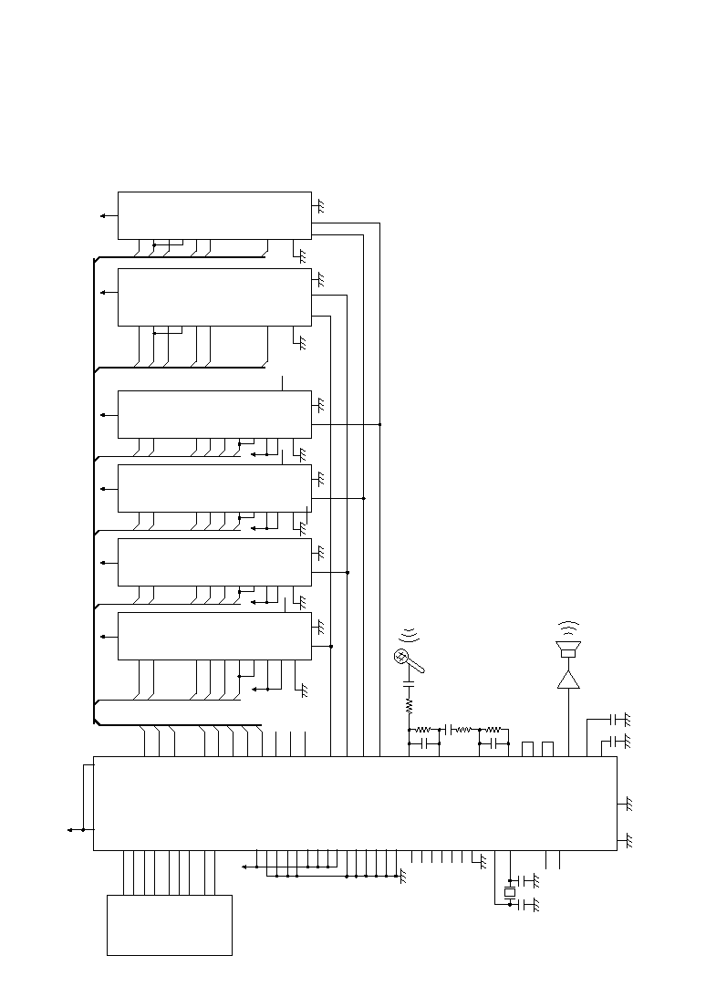
° Semiconductor
MSM6789A/6789L
APPLICATION CIRCUITS (for MSM6789L (3.3 V Version))
This is an application circuit example when the MSM6789L is used in microcontroller interface mode
with four 4-Mbit serial registers and two 2-Mbit serial voice ROMs.
Circuit
9
:
Application circuit in microcontroller interface mode with 4-Mbit
serial registers and 2-Mbit serial voice ROMs.
+
DGND
+
D3
MCUM
RSEL1
RSEL2
CE TEST
BUSY
RPM
VPM
XT
XT
MON
NAR
AGND
SG
SGC
AOUT
ADIN
FOUT
FIN
AMON
LOUT
LIN
MOUT
MIN
CS4
CS3
CS2
CS1
DROM
DI/O
WE
RWCK
TAS
SADY
SAS
SADX
AV
DD
DV
DD
Speaker drive amplifier
RECORDER IC MSM6789L
D2
D1
D0
RD WR CE
RESET
PDWN
Microcontroller
SYNC
TDT0-7
TMD0-3
TMD4
SADX
SAD
SAS
SAS
TAS
TAS
RWCK
RWCK
WE
WE
DI/O
DIN
DOUT
TEST
RS/A
CS
V
SS
V
CC
SADX
SADX
SAS
SASX
TAS
TAS
RWCK
RDCK
DOUT
TEST
CS1
CS2
V
CC
SADY
SADY
SASY
DROM
V
SS
8.192 MHz
4M Serial Register MSM66V84B
MSM66V84B
MSM66V84B
MSM66V84B
2M Serial Voice ROM
MSM6596A-XXX
MSM6596A-XXX
RFSH
NC
LOWPWR
DRAM/
SR
MSEL2
MSEL1
TST
TCK
TEST
EXTD
ACON
4B/
1B
CAS0
-
CAS7
RAS
A5-A10