 | –≠–ª–µ–∫—Ç—Ä–æ–Ω–Ω—ã–π –∫–æ–º–ø–æ–Ω–µ–Ω—Ç: MBF9412B | –°–∫–∞—á–∞—Ç—å:  PDF PDF  ZIP ZIP |
D
ATA
S
HEET
MBF9411B/9412B
Surface Acoustic Wave (SAW) Filters
for Mobile and Portable Phones
September 1998
O K I C O M M U N I C A T I O N S P R O D U C T S

s
MBF93xx
s
≠≠≠≠≠≠≠≠≠≠≠≠≠≠≠≠≠≠≠≠≠≠≠≠≠≠≠≠≠≠≠≠≠≠≠≠≠≠≠≠≠≠≠≠≠≠≠≠≠≠≠≠≠≠≠≠≠≠≠≠≠≠≠≠≠≠≠≠≠≠≠≠≠≠≠≠≠≠≠≠≠≠≠≠
Oki Semiconductor

1
Oki Semiconductor
MBF9411B/9412B
Surface Acoustic Wave (SAW) Filters
DESCRIPTION
The new MBF9411B/9412B Surface Acoustic Wave (SAW) filters use Oki's third generation design and
manufacturing technology to achieve a high out-of-band attenuation, low insertion loss, and low manu-
facturing cost in an industry standard 6-pin package, 1.2-mm thick and 3.0-mm square.
These 50-
matched bandpass microwave RF filters are designed for the worldwide standard wireless
voice and data communications frequencies being used by cellular and wireless local-loop service pro-
viders. They have achieved design acceptance by leading wireless handset manufacturers in North
America, Europe, and Asia.
Oki's lowest insertion loss SAW filters and high performance GaAs devices are used to reduce transmit-
ter complexity. Receiver designs can be simplified by using the higher Tx frequency attenuation SAW
filters.
These devices take advantage of Oki's 16-year plus RF communications component manufacturing expe-
rience and very high volume manufacturing capability to meet customer demands.
FEATURES
SAW Filter Summary
[1]
1.
All parts in 6-pin ceramic square package (3.0 mm x 3.0 mm) by 1.2-mm thick with system matched 50-
I/O
Part
Number
Description
Pass
Frequency
(MHz)
Insertion
Loss
(dB)
Stop
Frequency
(MHz)
Attenuation
(dB)
MBF9411B
CDMA Transmit Filter
824 to 849
<3.5
869 to 1049
>30
MBF9412B
CDMA Receive Filter
869 to 894
<3.5
779 to 849
>30
∑ Low insertion loss
∑ Small size, light weight
∑ 50-
matched
∑ 6-pin SMD package
∑ High reliability

s
MBF9411B/9412B
s
≠≠≠≠≠≠≠≠≠≠≠≠≠≠≠≠≠≠≠≠≠≠≠≠≠≠≠≠≠≠≠≠≠≠≠≠≠≠≠≠≠≠≠≠≠≠≠≠≠≠≠≠≠≠≠≠≠≠≠≠≠≠≠≠≠≠≠≠≠≠≠≠≠≠≠≠
2
Oki Semiconductor
PIN CONFIGURATION
BLOCK DIAGRAM
0.6
3.0
1.2 TYP
1.2 TYP
1.0
3.0
0.3
1.2
1.2
5
6
4
1
1
6
5
4
2
3
2
3
Pin
Number
Signal
1, 3, 4, 6
Ground
2
Input
5
Output
Dimensions in mm.
Rx-BPF
Tx-BPF
Rx-BPF
SAW
RF Amp
DUPLEXER
Power Amp
Tx-BPF
SAW
Mixer
IF-BPF
RF Amp
Mixer
VCO
MOD
IF Amp
DEMO
Ant
VCO

≠≠≠≠≠≠≠≠≠≠≠≠≠≠≠≠≠≠≠≠≠≠≠≠≠≠≠≠≠≠≠≠≠≠≠≠≠≠≠≠≠≠≠≠≠≠≠≠≠≠≠≠≠≠≠≠≠≠≠≠≠≠≠≠≠≠≠≠≠≠≠≠≠≠≠
s
MBF9411B/9412B
s
3
Oki Semiconductor
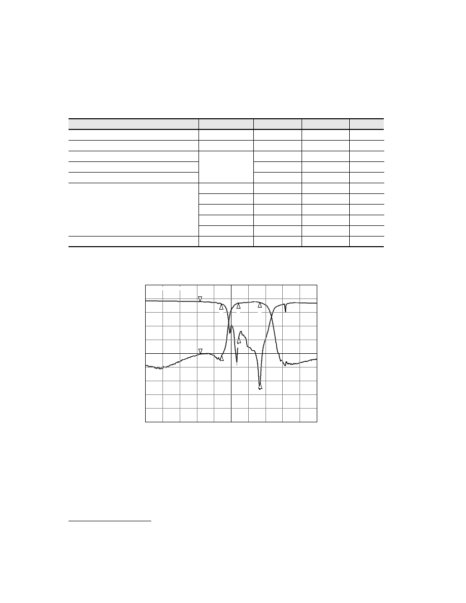
ELECTRICAL CHARACTERISTICS
MBF9411B Electrical Characteristics (-40 to +85∞C)
Parameter
Frequency (MHz)
Min.
Max.
Units
Center Frequency (F
C
)
Fr 836.5
≠
≠
MHz
Bandwidth (BW)
Fr ±12.5
≠
≠
MHz
Insertion Loss across BW
824 to 849
≠
3.5
dB
Return Loss across BW
8.5
≠
dB
Stop Band Attenuation
0.3 to 850
28
≠
dB
869 to 1049
30
≠
dB
1049 to 2000
20
≠
dB
Terminating Impedance
≠
50
ohms
Figure 1. MBF9411B Frequency Response
CENTER
860.000 000 MHZ
SPAN
200.000 000 MHZ
CH1
CH2
S11
S21
log MAG
log MAG
5 dB/
10 dB/
REF 0 db
REF 0 db
CDMA TX
Cor
Hld
Cor
Hld
2
3
4
2
3
4
1
1
2
1
1. ≠11.571 dB
1. ≠2.6971 dB
824.000 000 MHz
3. ≠1.7294 dB
869 MHz
4. ≠1.1989 dB
894 MHz
4. ≠42.015 dB
894 MHz
3. ≠49.21 dB
869 MHz
2. ≠2.0891 dB
849 MHz
2. ≠19.721 dB
849 MHz
s
MBF9411B/9412B
s
≠≠≠≠≠≠≠≠≠≠≠≠≠≠≠≠≠≠≠≠≠≠≠≠≠≠≠≠≠≠≠≠≠≠≠≠≠≠≠≠≠≠≠≠≠≠≠≠≠≠≠≠≠≠≠≠≠≠≠≠≠≠≠≠≠≠≠≠≠≠≠≠≠≠≠≠
4
Oki Semiconductor
MBF9412B Electrical Characteristics (-30 to +85∞C)
Parameter
Frequency (MHz)
Min.
Max.
Units
Center Frequency (F
C
)
Ft 881.5
≠
≠
MHz
Bandwidth (BW)
Fr ±12.5
≠
≠
MHz
Insertion Loss across BW
869 to 894
≠
3.5
dB
Ripple across BW
≠
2.0
dB
VSWR across BW
≠
2.0
dB
Stop Band Attenuation
500 to 779
25
≠
dB
779 to 849
30
≠
dB
914 to 939
20
≠
dB
939 to 1049
35
≠
dB
1049 to 2000
25
≠
dB
Terminating Impedance
≠
50
ohms
Figure 2. MBF9412B Frequency Response
START
760.000 000 MHz
STOP
960.000 000 MHz
CH1
CH2
S11
S21
log MAG
log MAG
5 dB/
10 dB/
REF 0 db
REF 0 db
CDMA R≠INT
Cor
Hld
Cor
Hld
2
3
4
2
3
4
1
1
2
1
1. ≠.9518
dB
1. ≠40.088 dB
824.000 000 MHz
3. ≠13.744
dB
869 MHz
4. ≠31.116 dB
894 MHz
4. ≠2.3963 dB
894 MHz
3. ≠2.8434 dB
869 MHz
2. ≠41.148 dB
849 MHz
PASS
PASS
2. ≠1.8131 dB
894 MHz

Oki Semiconductor
The information contained herein can change without notice owing to product and/or technical improvements.
Please make sure before using the product that the information you are referring to is up-to-date.
The outline of action and examples of application circuits described herein have been chosen as an explanation of the standard action
and performance of the product. When you actually plan to use the product, please ensure that the outside conditions are reflected in
the actual circuit and assembly designs.
Oki assumes no responsibility or liability whatsoever for any failure or unusual or unexpected operation resulting from misuse, neglect,
improper installation, repair, alteration or accident, improper handling, or unusual physical or electrical stress including, but not limited
to, exposure to parameters outside the specified maximum ratings or operation outside the specified operating range.
Neither indemnity against nor license of a third party's industrial and intellectual property right,etc.is granted by us in connection with
the use of product and/or the information and drawings contained herein. No responsibility is assumed by us for any infringement of a
third party's right which may result from the use thereof.
When designing your product, please use our product below the specified maximum ratings and within the specified operating ranges,
including but not limited to operating voltage, power dissipation, and operating temperature.
The products listed in this document are intended for use in general electronics equipment for commercial applications (e.g.,office
automation, communication equipment, measurement equipment, consumer electronics, etc.).These products are not authorized for
use in any system or application that requires special or enhanced quality and reliability characteristics nor in any system or application
where the failure of such system or application may result in the loss or damage of property or death or injury to humans. Such
applications include, but are not limited to: traffic control, automotive, safety, aerospace, nuclear power control, and medical, including
life support and maintenance.
Certain parts in this document may need governmental approval before they can be exported to certain countries. The purchaser
assumes the responsibility of determining the legality of export of these parts and will take appropriate and necessary steps, at their
own expense, for export to another country.
Copyright 1997 Oki Semiconductor
Oki Semiconductor reserves the right to make changes in specifications at anytime and without notice. This information furnished by
Oki Semiconductor in this publication is believed to be accurate and reliable. However, no responsibility is assumed by OKI
Semiconductor for its use; nor for any infringements of patents or other rights of third parties resulting from its use. No license is
granted under any patents or patent rights of OKI.

Northwest Area
785 N. Mary Avenue
Sunnyvale, CA 94086
Tel: 408/720-8940
Fax: 408/720-8965
Southwest Area
2302 Martin Street
Suite 250
Irvine, CA 92715
Tel: 714/752-1843
Fax: 714/752-2423
Northeast Area
138 River Road
Shattuck Office Center
Andover, MA 01810
Tel: 508/688-8687
Fax: 508/688-8896
Southeast Area
1590 Adamson Parkway
Suite 220
Morrow, GA 30260
Tel: 404/960-9660
Fax: 404/960-9682
Oki R
EGIONAL
S
ALES
O
FFICES
Corporate Headquarters
785 N. Mary Avenue
Sunnyvale, CA 94086-2909
Tel: 408/720-1900
Fax: 408/720-1918
Oki Stock No:
Oki FAX Service:
Call toll free 1-800-OKI-6994
Oki Web Site:
http://www.okisemi.com
320075-001