
° Semiconductor
MSM5718C50/MD5764802
1/45
° Semiconductor
MSM5718C50/MD5764802
18Mb (2M
•
•
•
•
• 9) & 64Mb (8M •
•
•
•
• 8) Concurrent RDRAM
DESCRIPTION
The 18/64-Megabit Concurrent RambusTM DRAMs (RDRAMÆ) are extremely high-speed
CMOS DRAMs organized as 2M or 8M words by 8 or 9 bits. They are capable of bursting unlimited
lengths of data at 1.67 ns per byte (13.3 ns per eight bytes). The use of Rambus Signaling Level (RSL)
technology permits 600 MHz transfer rates while using conventional system and board design
methodologies. Low effective latency is attained by operating the two or four 2KB sense amplifiers
as high speed caches, and by using random access mode (page mode) to facilitate large block
transfers. Concurrent (simultaneous) bank operations permit high effective bandwidth using
interleaved transactions.
RDRAMs are general purpose high-performance memory devices suitable for use in a broad range
of applications including PC and consumer main memory, graphics, video, and any other
application where high-performance at low cost is required.
FEATURES
∑ Compatible with Base RDRAMs
∑ 600 MB/s peak transfer rate per RDRAM
∑ Rambus Signaling Level (RSL) interface
∑ Synchronous, concurrent protocol for block-oriented, interleaved (overlapped) transfers
∑ 480 MB/s effective bandwidth for random 32 byte transfers from one RDRAM
∑ 13 active signals require just 32 total pins on the controller interface (including power)
∑ 3.3 V operation
∑ Additional/multiple Rambus Channels each provide an additional 600 MB/s bandwidth
∑ Two or four 2KByte sense amplifiers may be operated as caches for low latency access
∑ Random access mode enables any burst order at full bandwidth within a page
∑ Graphics features include write-per-bit and mask-per-bit operations
∑ Available in horizontal surface mount plastic package (SHP32-P-1125-0.65-K)
E2G1059-39-21
This version: Feb. 1999
Previous version: Nov. 1998

° Semiconductor
MSM5718C50/MD5764802
2/45
PART NUMBERS
The 18- and 64-Megabit RDRAMs are available in horizontal surface mount plastic package (SHP),
with 533 and 600 MHz clock rate. The part numbers for the various options are shown in Table 1.
Table 1 Part Numbers by Option
533 MHz
Options
600 MHz
18-Megabit SHP
64-Megabit SHP
MSM5718C50-53GS-K
MD5764802-53MC
MSM5718C50-60GS-K
MD5764802-60MC
° Semiconductor
MSM5718C50/MD5764802
3/45
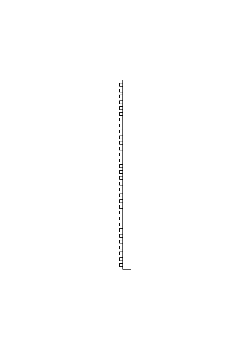
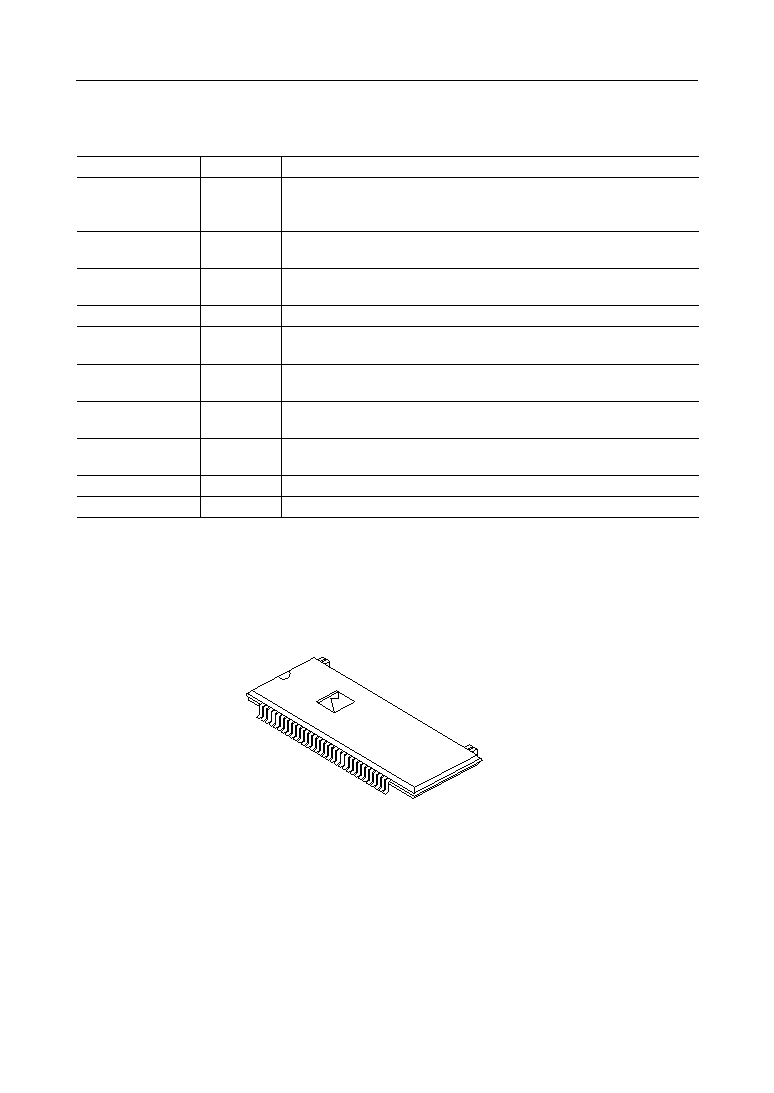
RDRAM PACKAGES AND PINOUTS
RDRAMs are available in horizontal surface mount plastic package (SHP).
The package has 32 signal pins and four mechanical pins that provide support for the device. The
mechanical pins are located on the opposite side from the signal leads in the SHP.
VDD
1
GND
2
DQ8
3
GND
4
DQ7
5
NC (18M) ; VREF (64M)
6
ADDRESS
7
VDD
8
DQ6
9
GND
10
DQ5
11
VDDA
12
RXCLK
13
GNDA
14
TXCLK
15
VDD
16
DQ4
17
GND
18
COMMAND
19
SIN
20
VREF
21
SOUT
22
DQ3
23
GND
24
DQ2
25
(NC)
26
DQ1
27
GND
28
DQ0
29
(NC)
30
GND
31
VDD
32
Fig. 1 SHP Pin Numbering
° Semiconductor
MSM5718C50/MD5764802
4/45
Table 2 Pin Descriptions
Signal lines for REQ, DIN, and DOUT packets. The REQ packet contains the
address field, command field, and other control fields. These are RSL
signals.
a
Signal
I/O
Description
DQ8..DQ0
(BUSDATA [8:0])
I/O
Receive clock. All input packets are aligned to this clock. This is an RSL
signal.
a
CLK
(RXCLK)
I
Transmit clock. DOUT packets are aligned with this clock. This is an RSL
signal.
a
CLK
(TXCLK)
I
Logic threshold reference voltage for RSL signals.
VREF
I
Signal line for REQ, RSTRB, RTERM, WSTRB, WTERM, RESET, and CKE
packets. This is an RSL signal.
a
COMMAND
(BUSCTRL)
I
Signal line for COL packets with column addresses. This is an RSL signal.
a
ADDRESS
(BUSENABLE)
I
+3.3 V power supply. VDDA is a separate analog supply for clock generation
in the RDRAM.
VDD, VDDA
Circuit ground. GNDA is a separate analog ground for clock generation in
the RDRAM.
GND, GNDA
Initialization daisy chain input. CMOS levels.
SIN
I
Initialization daisy chain output. CMOS levels.
SOUT
O
--
--
a. RSL stands for Rambus Signaling Levels, a low-voltage-swing, active-low signaling technology.
Pin 1
Pin 32
Mechanical
Support Pins
Mechanical
Support Pins
Fig. 2 SHP Package

° Semiconductor
MSM5718C50/MD5764802
5/45
GENERAL DESCRIPTION
Figure 3 is a block diagram of an RDRAM. At the bottom is a standard DRAM core organized as two
or four independent banks, with each bank organized as 512 or 1024 rows, and with each row
consisting of 2KBytes of memory cells. One row of a bank may be "activated" at any time (ACTV
command) and placed in the 2KByte "page" for the bank. Column accesses (READ and WRITE
commands) may be made to this active page.
The smallest block of memory that may be accessed with READ and WRITE commands is an octbyte
(eight bytes). Bitmask and bytemask options are available with the WRITE command to allow finer
write granularity. There are six control registers that are accessed at initialization time to configure
the RDRAM for a particular application.