
MG113P/114P/115P/73P/74P/75P
0.25µm Sea of Gates and
Customer Structured Arrays
August 2002
O
K
I
A
S
I
C
P
R
O
D
U
C
T
S
D
ATA
S
HEET

Oki Semiconductor
I
I
≠≠≠≠≠≠≠≠≠≠≠≠≠≠≠≠≠≠≠≠≠≠≠≠≠≠≠≠≠≠≠≠≠≠≠≠≠≠≠≠≠≠≠≠≠≠≠≠≠≠≠≠≠≠≠≠≠≠≠≠≠≠≠≠≠≠≠≠≠≠≠≠≠≠≠≠≠≠≠≠≠≠≠≠≠≠≠≠≠≠≠
CONTENTS
MG113P/114P/115P/73P/74P/75P Family Listing ........................................................................................... 2
Array Architecture ...................................................................................................................................................2
MG73P/74P/75P CSA Layout Methodology ................................................................................................3
Electrical Characteristics ........................................................................................................................................ 5
Macro Library ...........................................................................................................................................................9
Macrocells for Driving Clock Trees ...............................................................................................................10
Oki Advanced Design Center Cad Tools ............................................................................................................ 11
Design Process .................................................................................................................................................12
Automatic Test Pattern Generation ...............................................................................................................13
Floorplanning Design Flow ...........................................................................................................................13
IEEE JTAG Boundary Scan Support .............................................................................................................15
Package Options .................................................................................................................................................... 16
1
Oki Semiconductor
MG113P/114P/115P/73P/74P/75P
0.25µm Sea of Gates and Customer Structured Arrays
DESCRIPTION
Oki's 0.25µm Application-Specific Integrated Circuit (ASIC) products are available in both Sea Of Gates
(SOG) and Customer Structured Array (CSA) architectures. Both the SOG-based MG115P series and the
CSA-based MG75P series use a five-layer metal process on 0.25µm drawn (0.18µm L-effective) CMOS
technology. The SOG MG113P/114P series uses the same SOG base-array architecture as the MG115P
series, but offers four and three metal layers, respectively. The MG73P/74P CSA series uses three and
four metal layers, respectively. The semiconductor process is adapted from Oki's production-proven 64-
Mbit DRAM manufacturing process.
The 0.25µm family provides significant performance, density, and power improvement over previous
0.35µm technologies. An innovative 4-transistor cell structure, licensed from In-Chip Systems, Inc., pro-
vides 30 to 50% less power and 30 to 50% more usable gates than traditional cell designs. The Oki 0.25µm
family operates using 2.5-V V
DD
core with optimized 3-V I/O buffers. The 3-, 4-, and 5-layer metal
MG113P/114P/115P SOG series contains 4 array bases, offering up to 588 I/O pads and over 2.4M raw
gates. The 3-, 4-, and 5-layer metal MG73P/74P/75P CSA series contains 21 array bases, offering up to
868 I/O pads and over 5.4M raw gates. These SOG and CSA array sizes are designed to fit the most pop-
ular quad flat pack (QFP), low profile QFPs (LQFPs), thin QFPs (TQFPs), plastic ball grid array (PBGA),
and metal ball grid array (MBGA) packages.
The MG113P/114P/115P series SOG architecture allows rapid prototyping turnaround times (TATs),
additionally offering the most cost-effective solution for pad-limited circuits (particularly the 3-layer
metal MG113P series). The 3-layer-metal MG73P, 4-layer-metal MG74P and 5-layer-metal MG75P CSA
series contains 21 array bases, offering a wider span of gate and I/O counts than the SOG series. Oki uses
the Artisan Components memory compiler which provides high performance, embedded synchronous
single- and dual-port RAM macrocells for CSA designs. As such, the MG73P/74P/75P series is suited to
memory-intensive ASICs and high-volume designs where fine tuning of package size produces signifi-
cant cost or real-estate savings.
FEATURES
∑ 0.25µm drawn 3-, 4-, and 5-layer metal CMOS
∑ Optimized 2.5-V core
∑ Optimized 3-V I/O
∑ Optimized 5-V Tolerant I/O
∑ SOG and CSA architecture availability
∑ 61-ps typical gate propagation delay (for a 4x-
drive inverter gate with a fanout of 2 and 0 mm
of wire, operating at 2.5 V)
∑ Over 5.4M raw gates and 868 I/O pads using
60µ staggered I/O
∑ User-configurable I/O with V
SS
, V
DD
, TTL,
3-state, and 1- to 24-mA options
∑ Slew-rate-controlled outputs for low-radiated noise
∑ Clock tree cells which reduces the maximum
skew for clock signals
∑ Gated clock
∑ Low 0.2µW/MHz/gate power dissipation
∑ User-configurable single- and dual-port
memories
∑ Specialized IP cores and macrocells including
32-bit ARM7TDMI CPU, phase-locked loop
(PLL), and peripheral component interconnect
(PCI) cells
∑ Floorplanning for front-end simulation, back-
end layout controls, and link to synthesis
∑ Joint Test Action Group (JTAG) boundary scan
and scan path Automatic Test Pattern
Generation (ATPG)
∑ Built-In Self Test (BIST) for memory testing
∑ Support for popular CAE systems including
Cadence, Model Technology, Inc. (MTI), Zycad
and Synopsys
2
Oki Semiconductor
I
MG113P/114P/115P/73P/74P/75P
I
≠≠≠≠≠≠≠≠≠≠≠≠≠≠≠≠≠≠≠≠≠≠≠≠≠≠≠≠≠≠≠≠≠≠≠≠≠≠≠≠≠≠≠≠≠≠≠≠≠≠≠≠≠≠≠≠≠≠≠≠≠≠≠≠
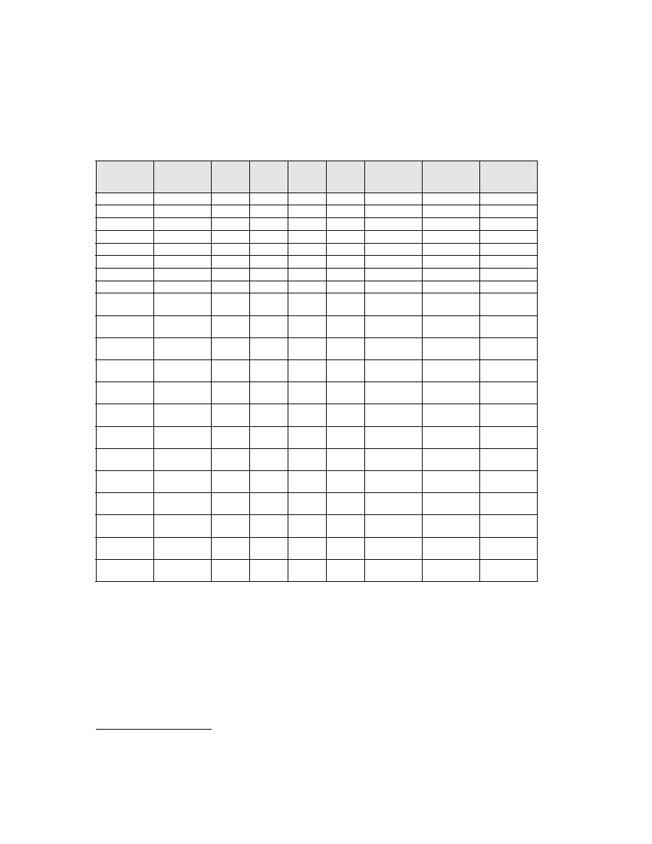
MG113P/114P/115P/73P/74P/75P FAMILY LISTING
ARRAY ARCHITECTURE
The primary components of a 0.25µm MG113P/114P/115P/73P/74P/75P circuit include:
∑ I/O base cells
∑ 60µm pad pitch
∑ Configurable I/O pads for V
DD
, V
SS
, or I/O (optimized 3-V I/O)
∑ V
DD
and V
SS
pads dedicated to wafer probing
∑ Separate power bus for output buffers
∑ Separate power bus for internal core logic and input buffers
SOG Base
Array
EA Base
Array
No. of
Pads
No. of
Rows
No. of
Column
s
No. of
Raw
Gates
MG113P/73P
Family 3LM
Usable Gates
MG114P/74P
Family 4LM
Usable Gates
MG115P/75P
Family 5LM
Usable Gates
MG7xPB02
68
84
280
23,520
22,344
22,344
MG7xPB04
108
144
480
69,120
65,664
65,664
MG7xPB06
148
204
680
138,720
131,784
131,784
MG7xPB08
188
264
880
232,320
218,381
220,704
MG7xPB10
228
324
1,080
349,920
311,429
332,424
MG7xPB12
268
384
1,280
491,520
412,877
466,944
MG11xP14
MG7xPB14
308
444
1,480
657,120
387,701
519,125
611,122
MG7xPB16
348
504
1,680
846,720
635,040
745,114
MG11xP18
MG7xPB18
388
564
1,880
1,060,32
0
572,573
763,430
901,272
MG7xPB20
428
624
2,080
1,297,92
0
882,586
1,025,357
MG11xP22
MG7xPB22
468
684
2,280
1,559,92
0
732,974
982,498
1,154,045
MG7xPB24
508
744
2,480
1,845,12
0
1,107,072
1,310,035
MG7xPB26
548
804
2,680
2,154,72
0
1,249,738
1,465,210
MG11xP28
MG7xPB28
588
864
2,880
2,488,32
0
1,094,861
1,393,459
1,642,291
MG7xPB30
628
924
3,080
2,845,92
0
1,536,797
1,821,389
MG7xPB32
668
984
3,280
3,227,52
0
1,678,310
2,001,062
MG7xPB34
708
1,044
3,480
3,633,12
0
1,816,560
2,179,872
MG7xPB36
748
1,104
3,680
4,062,72
0
1,950,106
2,356,378
MG7xPB38
788
1,164
3,880
4,516,32
0
2,077,507
2,529,139
MG7xPB40
828
1,224
4,080
4,993,92
0
2,197,325
2,696,717
MG7xPB42
868
1,284
4,280
5,495,52
0
2,308,118
2,857,670
3
Oki Semiconductor
≠≠≠≠≠≠≠≠≠≠≠≠≠≠≠≠≠≠≠≠≠≠≠≠≠≠≠≠≠≠≠≠≠≠≠≠≠≠≠≠≠≠≠≠≠≠≠≠≠≠≠≠≠≠≠≠≠≠≠≠≠≠≠
I
MG113P/114P/115P/73P/74P/75P
I
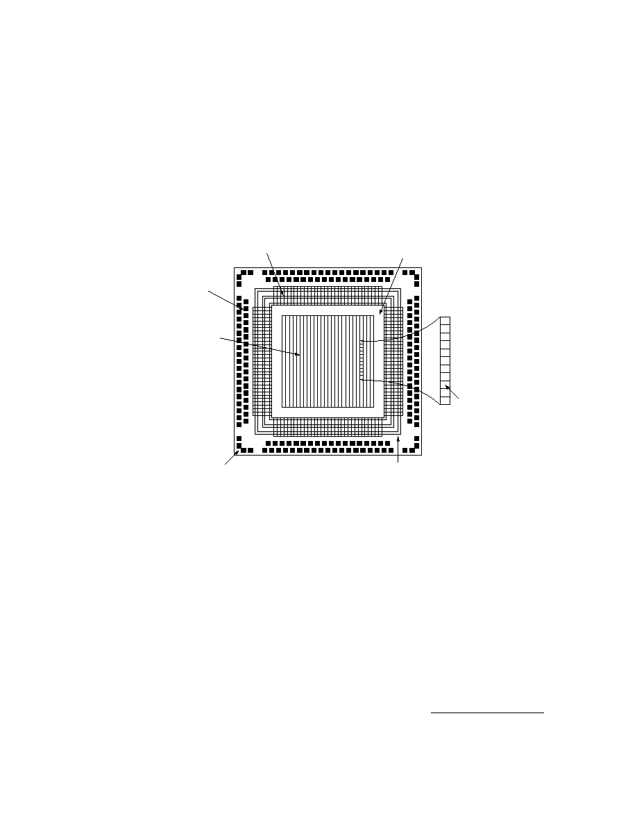
∑ Core base cells containing N-channel and P-channel pairs, arranged in column of gates
∑ Isolated gate structure for reduced input capacitance and increased routing flexibility
∑ Innovative 4-transistor core cell architecture, licensed from In-Chip Systems, Inc
Each array has 24 dedicated corner pads for power and ground use during wafer probing, with four pads
per corner. The arrays also have separate power rings for the internal core functions (V
DDC
and V
SSC
)
and output drive transistors (V
DDO
and V
SSO
).
MG73P/74P/75P CSA Layout Methodology
The procedure to design, place, and route a CSA follows.
1. Select suitable base array frame from the available predefined sizes. To select an array size:
- Identify macrocell functions required and minimum array size to hold macrocell functions.
- Add together all the area occupied by the required random logic and macrocells and select
the optimum array.
2. Make a floor plan for the design's megacells.
- Oki Design Center engineers verify the master slice and review simulation.
- Oki Design Center or customer engineers floorplan the array using Oki's supported floor-
planner and customer performance specifications.
Core base cell
with 4 transistors
Separate power bus (V
DDO
, V
SSO
) over I/O cell
for output buffers (2nd metal/3rd metal)
V
DD
, V
SS
pads (4) in each
corner for wafer probing only
Configurable I/O pads
for V
DD
, V
SS
, or I/O
Separate power bus (V
DDC
, V
SSC
) for
internal core logic (2nd metal/3rd metal)
I/O base cells
1, 2, 3, 4, or 5 layer
metal
interconnection in
core area
Figure 1. MG115P Array Architecture