
MK31VT872A-8YC
—
98.06.26
“
Semiconductor
MK31VT872A-8YC
8,388,608 Word x 72 Bit SYNCHRONOUS DYNAMIC RAM MODULE (1BANK):
DESCRIPTION
The Oki MK31VT872A-8YC is a fully decoded, 8,388,608 x 72bit synchronous dynamic
random access memory composed of eight 64Mb DRAMs(8Mx9) in TSOP packages
mounted with decoupling capacitors on a 168-pin glass epoxy Dual-in-Line Package
supports any application where high density and large capacity of storage memory are
required, like for example PCs or servers.
FEATURES
∑
8-Meg Word x 72-Bit (1Bank 8 Byte) organization
∑
168-pin Dual Inline Memory Module
∑
All DQ Pins have 10
Damping Resister
∑
Single 3.3V power supply, ±0.3V tolerance
∑
Input
:LVTTL compatible
∑
Output
:LVTTL compatible
∑
Refresh : 4,096 cycles/64 ms
∑
Programmable data transfer mode
∑
/CAS latency(2, 3)
∑
Burst length(1,2,4,8,Full page)
∑
Data scramble(sequential,interleave)
∑
/CAS before /RAS auto-refresh, Self-refresh capability
∑
Serial Presence Detect (SPD) With EEPROM
PRODUCT ORGANIZATION
Operation
Access Time(Max.)
Product Name
Frequency(Max.)
tAC2
tAC3
MK31VT872A - 8YC
125 MHz
10.0ns
6.0ns
MK31VT872A-8YC
—
98.06.26
“
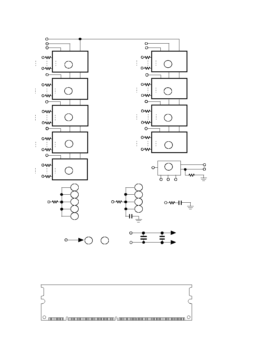
BLOCK DIAGRAM
5
/CS0
CKE0
DQMB0
DQMB1
DQ0
DQ7
DQ0
DQ7
DQ8
DQ15
DQMB4
DQ0
DQ7
DQM
CKE
/CS
DQM
CKE
/CS
DQ40
DQ47
DQMB5
DQMB2
DQMB3
DQ0
DQ7
DQ16
DQ23
DQ0
DQ7
DQ24
DQ31
DQMB7
DQ0
DQ7
DQ48
DQ55
DQ0
DQ7
DQ56
DQ63
DQM
CKE
/CS
DQM
CKE
/CS
DQM
CKE
/CS
DQM
CKE
/CS
/CS2
DQMB6
DQ0
DQ7
DQM
CKE
/CS
DQ32
DQ39
DQ0
DQ7
DQM
CKE
/CS
Vcc
Vss
Two Decoupling Capacitors
per SDRAM
0.1uF
0.33uF
/RAS,/CAS,/WE
A0-A15 & BA0,BA1
·
1
9
SCL
SDA
A0 A1 A2
SA0 SA1 SA2
Serial PD
CLK2
3.3pF
3
4
CLK0
1
2
7
8
3
4
WP
47K
4
6
7
1
9
8
2
10
3
CLK1
CLK3
10pF
DQ0
DQ7
DQM
CKE
/CS
CB0
CB7
5
DQMB1
Note. The Value of all resistors is 10
expect WP
MODULE OUTLINE
(Front)
(Back)
1
85
10
94
11
95
40
124
41
125
84
168

MK31VT872A-8YC
—
98.06.26
“
PIN CONFIGURATION
Front side
Back side
Front side
Back side
Pin No.
Pin name
Pin No.
Pin name
Pin No.
Pin name
Pin No.
Pin name
<
VSS
85
VSS
43
VSS
127
VSS
2
DQ0
86
DQ32
44
N.C
128
CKE0
3
DQ1
87
DQ33
45
/CS2
129
N.C
4
DQ2
88
DQ34
46
DQMB2
130
DQMB6
5
DQ3
89
DQ35
47
DQMB3
131
DQMB7
6
VCC
90
VCC
48
N.C
132
N.C
7
DQ4
91
DQ36
49
VCC
133
VCC
8
DQ5
92
DQ37
50
N.C
134
N.C
9
DQ6
93
DQ38
51
N.C
135
N.C
10
DQ7
94
DQ39
52
CB2
136
CB6
11
DQ8
95
DQ40
53
CB3
137
CB7
12
VSS
96
VSS
54
VSS
138
VSS
13
DQ9
97
DQ41
55
DQ16
139
DQ48
14
DQ10
98
DQ42
56
DQ17
140
DQ49
15
DQ11
99
DQ43
57
DQ18
141
DQ50
16
DQ12
100
DQ44
58
DQ19
142
DQ51
17
DQ13
101
DQ45
59
VCC
143
VCC
18
VCC
102
VCC
60
DQ20
144
DQ52
19
DQ14
103
DQ46
61
N.C
145
N.C
20
DQ15
104
DQ47
62
N.C
146
N.C
21
CB0
105
CB4
63
N.C
147
N.C
22
CB1
106
CB5
64
VSS
148
VSS
23
VSS
107
VSS
65
DQ21
149
DQ53
24
N.C
108
N.C
66
DQ22
150
DQ54
25
N.C
109
N.C
67
DQ23
151
DQ55
26
VCC
110
VCC
68
VSS
152
VSS
27
/WE
111
/CAS
69
DQ24
153
DQ56
28
DQMB0
112
DQMB4
70
DQ25
154
DQ57
29
DQMB1
113
DQMB5
71
DQ26
155
DQ58
30
/CS0
114
N.C
72
DQ27
156
DQ59
31
N.C
115
/RAS
73
VCC
157
VCC
32
VSS
116
VSS
74
DQ28
158
DQ60
33
A0
117
A1
75
DQ29
159
DQ61
34
A2
118
A3
76
DQ30
160
DQ62
35
A4
119
A5
77
DQ31
161
DQ63
36
A6
120
A7
78
VSS
162
VSS
37
A8
121
A9
79
CLK2
163
CLK3
38
A10
122
BA0
80
N.C
164
N.C
39
BA1
123
A11
81
WP
165
SA0
40
VCC
124
VCC
82
SDA
166
SA1
41
VCC
125
CLK1
83
SCL
167
SA2
42
CLK0
126
N.C
84
VCC
168
VCC
Pin Name
Function
Pin Name
Function
VCC
Power Supply (3.3V)
/WE
Write Enable
VSS
Ground (0V)
DQMB#
Data Input / Output Mask
CLK#
System Clock
DQ# , CB#
Data Input / Output
/CS#
Chip Select
WP
Write Protect
CKE#
Clock Enable
SDA
Data I/O for SPD
A0-A11
Address
SCL
CLK input for SPD
BA0,BA1
Bank Select Address
SA#
Socket Position Address for SPD
/RAS
Row Address Strobe
N.C
No Connection
/CAS
Column Address Strobe

MK31VT872A-8YC
—
98.06.26
“
SERIAL PRESENCE DETECT
Byte
No.
SPD
Hex Value
Remark
Notes
0
80
Defines the number of bytes written into
SPD memory
128 byte
1
08
Total number of bytes of SPD memory
256 byte
2
04
Fundamental memory type
SDRAM
3
0C
Number of rows
12 rows
4
09
Number of columns
9 columns
5
01
Number of module banks
1 bank
6
48
Data width of this assembly
72 bits
7
00
... Data width continuation
0
8
01
Voltage interface level
LVTTL
9
80
Cycle time (CL=3)
CL=3 tCC=8ns
10
60
Access time from CLK (CL=3)
CL=3 tAC3=6ns
11
02
DIMM configuration type
ECC
12
80
Refresh rate / type
Normal/ Self/
13
08
Primary SDRAM width
x8
14
08
Error checking SDRAM width
x8
15
01
Minimum CLK delay
tCCD: 1 CLK
16
8F
Burst lengths supported
1,2,4,8,F
17
04
Number of banks on each SDRAM
4 banks
18
06
/CAS latency
2,3
19
01
/CS latency
0
20
01
/WE latency
0
21
00
SDRAM module attributes
22
0E
SDRAM device attributes : General
23
C0
Cycle time (CL=2)
CL=2 tCC2=12ns
24
A0
Access time from CLK (CL=2)
CL=2 tAC2=10ns
25
00
Cycle time (CL=1)
Not support
26
00
Access time from CLK (CL=1)
Not support
27
1E
Minimum ROW pulse width
tRP=30ns
28
10
/RAS to /RAS bank delay
tRRD=16ns
29
14
/RAS to /CAS delay
tRCD=20ns
30
30
Minimum /RAS precharge time
tRAS=48ns
31
10
Density of each bank on module
64MB
32
20
Command and address signal input setup time
2ns
33
10
Command and address signal input hold time
1ns
34
20
Data signal input setup time
2ns
35
10
Data signal input hold time
1ns
36-61
00-00
R.F.U
62
12
SPD data revision code
1.2
63
5B
Checksum for byte 0-62
64-71
41,45,20,20,20,20,20,20
Manufacturer's JEDEC ID code
72
01/06
Manufacturing location
73-90
4D,4B,33,31,56,54,38,37,32,
41,2D,38,59,43,20,20,20,202
Manufacturer's part number
MK31VT872A-8YC
91,92
20,20
Revision code
93-125
00-00
R.F.U
126
64
Intel specification frequency
100MHz
127
A5
Intel specification /CAS latency
(CLK0-2,CL=3)
128-255
FF-FF
Unused storage locations
MK31VT872A-8YC
—
98.06.26
“
ELECTRICAL CHARACTERISTICS
Absolute Maximum Ratings
Rating
Symbol
Value
Unit
Voltage on any pin relative to Vss
VIN, VOUT
-0.5 to VCC+0.5
V
Vcc supply voltage
Vcc,VccQ
-0.5 to 4.6
V
Storage temperature
Tstg
- 55 to 125
∞C
Power dissipation
PD*
9
W
Short circuit current
Ios
50
mA
Operating temperature
Topr
0 to 70
∞C
*: Ta=25
∞C
Recommended Operating Conditions
(Voltages referenced to Vss = 0V)
Parameter
Symbol
Min.
Typ.
Max.
Unit
Power supply voltage
Vcc,VccQ
3.0
3.3
3.6
V
Input high voltage
VIH
2.0
-
VCC+0.3
V
Input low voltage
VIL
-0.3
-
0.8
V
Capacitance
(Vcc=3.3V
±
0.3V,Ta=25 ∞C f=1MHz)
Parameter
Symbol
Max.
Unit
Input capacitance(A0-A11,BA0,BA1,/RAS, /CAS,/WE)
CIN1
54
pF
Input capacitance(/CS0,/CS2)
CIN2
34
pF
Input capacitance(DQMB0-DQMB7)
CIN3
16
pF
Input capacitance(CKE0)
CIN4
58
pF
I/O capacitance(DQ0-DQ63,CB0 - CB7)
C
I/O
18
pF
Input capacitance(CLK0,CLK2)
C
CLK
50
pF