 | –≠–ª–µ–∫—Ç—Ä–æ–Ω–Ω—ã–π –∫–æ–º–ø–æ–Ω–µ–Ω—Ç: ML2201-XX | –°–∫–∞—á–∞—Ç—å:  PDF PDF  ZIP ZIP |

1/22
MSM9831-xxx
° Semiconductor
GENERAL DESCRIPTION
MSM9831 is a PCM-based Voice Synthesis LSI (Playback only) with on-chip 384Kbit Mask ROM,
D/A Converter and Low-Pass Filter.
Serial input interface for an external MCU makes MSM9831 a better choice for size-critical
applications with less wiring pin-count in small foot-print packaging.
FEATURES
∑ 8-bit OKI Non-Linear PCM Algorithm
∑ Sampling Frequency (Selectable on each phrase)
4.0/5.3/6.4/8.0/10.6/12.8/16.0 kHz
∑ On-chip Mask ROM Capacity
: 384 Kbits
∑ Maximum Playback Time Length
12.0 sec.
at fsam
= 4.0 kHz
6.0 sec.
at fsam
= 8.0 kHz
3.0 sec.
at fsam
= 16.0 kHz
∑ Clock Oscillation
3.5 to 4.5 MHz (Ceramic Oscillation)
3.5 to 17 MHz (External Clock)
∑ User definable Phrase Control Table function
∑ Maximum number of Phrases
: 31 phrases
∑ 10-bit current-output-type D/A Converter
∑ A built-in LPF
∑ Power Supply Voltage
: +2.0 to +5.5 V (External Clock)
+2.5 to +5.5V (Ceramic Oscillation)
∑ Package:
8-Pin SOP Package (SOP8-P-250-1.27-K) (Product name: MSM9831-xxx MA)
COMPARISON TABLE WITH MSM9802
° Semiconductor
MSM9831-xxx
VOICE SYNTHESIS LSI with on-chip 384Kbit MASK ROM
MSM9831
Mask ROM Capacity
384K Bit
Interface
MCU (Serial)
Oscillation
Ceramic/External Clock
Max. Phrase Number
31
D/A Converter Current Flowing
Forced into the circuit
MSM9802
512K Bit
MCU (Parallel)/Stand-alone
Ceramic/CR
63
Forced out of the circuit
Status Signal Output
None
NAR/BUSY
E2D0097-19-94
This version: Sep. 1999

2/22
MSM9831-xxx
° Semiconductor
PIN CONFIGURATION (TOP VIEW)
ST
PI
GND
AOUT
PDWN
XT
XT
V
DD
1
2
3
4
8
7
6
5
8-pin Plastic SOP
BLOCK DIAGRAM
384-Kbit ROM
2-Kbit ROM
Phrase Control Table
2-Kbit ROM
Phrase Addres Table
Test ROM 2-Kbit
PCM data Area
378-Kbit
16-bit Address
controller
Serial
Interface
PCM
Synthesizer
10-bit DAC
LPF
AOUT
GND
V
DD
ST
PI
PDWN
Timing
Controller
OSC
Circuit
XT
XT
Reset, Power Down
10
8
8
8
16
5

3/22
MSM9831-xxx
° Semiconductor
PIN DESCRIPTIONS
Symbol
I/O
Description
ST
I
Playback starter pin.
Phrase Address (number) is determined by the number of times of input to
PI pin while ST being held "L". Playback starts on ST's rising edge with
phrase address data loaded into the LSI. When no pulse input to PImade
while ST being held "L", the LSI recognizes it as "Stop Code" to stop
playback.
PI
I
Address input pin.
The phrase number to playback is determined by the times of pulse pulse
input to PI pin while ST being held "L".
32-time pulse input has the internal counter initialized.
GND
--
GND pin.
AOUT
O
Analog output pin.
Built with N-MOS open-drain type, wave-form output is made in the form of
changing output current. While PDWN being held "H", AOUT maintains 1/2
level output, thus the current keeps on flowing.
The Pop-Noise Canceller is put into works when standby is reset to return to
be active, and when entering into standby mode.
V
DD
--
Power supply pin. Insert a 0.1mF or larger by-pass capacitor in-between GND
pin and this pin.
XT
I
Wired to the ceramic oscillator when a ceramic oscillator is in use.
Input the clock signal to this pin when the external clock is selected as the
timing source.
Using a ceramic oscillator or an external clock can be selected with OKI's
Analizing and Editing Tool.
PDWN
Pin
1
2
3
4
5
6
8
I
The LSI remains in standby mode while this pin is being held "L".
XT
7
O
Wired to the ceramic oscillator when a ceramic oscillator is in use.
When the external clock is in use, keep this pin open.
4/22
MSM9831-xxx
° Semiconductor
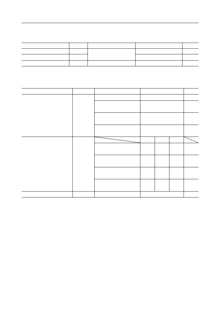
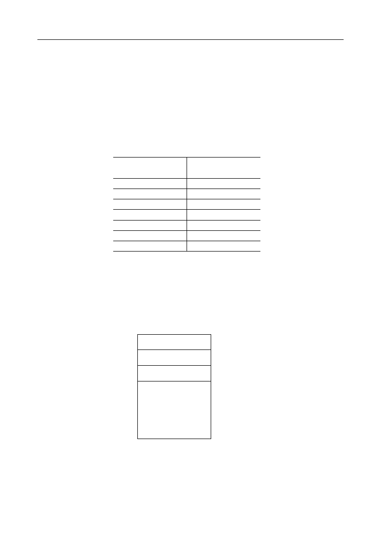
ABSOLUTE MAXIMUM RATINGS
RECOMMENDED OPERATING CONDITIONS
Parameter
Symbol
Condition
Rating
Unit
V
DD
V
IN
T
STG
Power Supply Voltage
Input Voltage
Storage Temperature
Ta = 25∞C
≠0.3 to +7.0
≠0.3 to V
DD
+0.3
≠55 to +150
V
V
∞C
--
(GND=0V)
Parameter
(GND=0V)
Symbol
Condition
Range
Unit
Power Supply Voltage
V
DD
With a Ceramic Osc. (
Note)
2.5 to 5.5
V
Master Clock Frequency
Typ.
4.096
Max.
4.5
Min.
3.5
f
OSC
With a Ceramic Osc.
MHz
With the external clock
f
OSC
=3.5 MHz to 4.5 MHz
2.0 to 5.5
V
With the external clock
f
OSC
=3.5 MHz to 14.5 MHz
2.7 to 5.5
V
With the external clock
f
OSC
=3.5 MHz to 17 MHz
3.0 to 5.5
V
Operating Temperature
T
op
--
≠40 to +85
∞C
4.096
4.5
3.5
With the external clock
V
DD
=2.0 V to 5.5 V
MHz
--
14.5
3.5
With the external clock
V
DD
=2.7 V to 5.5 V
MHz
--
17
3.5
With the external clock
V
DD
=3.0 V to 5.5 V
MHz
(Note)
V
DD
=2.5 V to 5.5 V
Note: A crystal that is usable in this LSI is described in "Functional Description" of this
document. If you want to use a different crystal, it is recommended to evaluate the crystal
before using it.

5/22
MSM9831-xxx
° Semiconductor
ELECTRICAL CHARACTERISTICS
DC Characteristics
Parameter
"H" Input Voltage
(V
DD
=2.0 to 5.0 V, GND=0 V, f
OSC
=4.096 MHz, Ta=≠40 to +85∞C, unless otherwise specified)
Symbol
Condition
Min.
Typ.
Max.
Unit
V
IH
f
OSC
=14.5 MHz or less
V
DD
• 0.8
--
--
V
"H" Input Current
I
IH
V
IH
=V
DD
--
--
10
mA
"L" Input Current
I
IL
V
IL
=GND
≠10
--
--
mA
Dynamic Supply
Current
I
DD
AOUT output
current is
excluded
--
1.2
3.0
mA
Standby Supply
Current
I
DS
Ta=≠40∞C to +70∞C
--
--
10
mA
Ta=≠40∞C to +85∞C
--
--
50
mA
AOUT Output
Current
I
AOUT
V
DD
=2.0 V to 5.5 V
0.4
--
8.9
mA
(V
DD
=2.7 V to 5.5 V)
f
OSC
=4.5 MHz or less
(V
DD
=2.0 V to 5.5 V)
V
DD
• 0.85
--
--
V
f
OSC
>14.5 MHz
(V
DD
=3.0 V to 5.5 V)
"L" Input Voltage
V
IL
--
--
V
DD
• 0.2
V
f
OSC
=4.5 MHz or less
(V
DD
=2.0 V to 5.5 V)
--
--
V
DD
• 0.15
V
f
OSC
>14.5 MHz
(V
DD
=3.0 V to 5.5 V)
f
OSC
=14.5 MHz or less (V
DD
=2.7 V to 5.5 V)
V
DD
=5.5 V
f
OSC
=4.096 MHz
--
0.4
1.0
mA
V
DD
=3.0 V
f
OSC
=4.096 MHz
--
0.2
0.7
mA
V
DD
=2.0 V
f
OSC
=4.096 MHz
--
--
12.0
mA
V
DD
=5.5 V
f
OSC
=16 MHz
--
--
4.0
mA
V
DD
=3.0 V
f
OSC
=16 MHz
--
--
2.8
mA
V
DD
=2.0 V
f
OSC
=16 MHz
V
DD
=5.5 V
3.8
6.0
8.9
mA
V
DD
=2.0 V
0.4
1.0
1.9
mA
At maximum
output current

6/22
MSM9831-xxx
° Semiconductor
AC Characteristics
Parameter
Master Clock duty cycle
(Oscillation Frequency at f
OSC
=4.096 MHz, V
DD
=2.0 to 5.0 V, GND=0 V, Ta=≠40 to +85∞C)
Symbol
Condition
Min.
Typ.
Max.
Unit
f
duty
--
40
50
60
%
Time before RESET input after Power On
t
RST
--
10
--
--
ms
PDWN hold time after RESET input
t
PDH
--
10
--
--
ms
DA Converter shifting time
(Pop-Noise Canceller working time)
t
DAR
, t
DAF
--
60
64
68
ms
PDWN-ST setup time
t
PDSS
--
1
--
--
ms
ST-PI setup time
t
SPS
--
1
--
--
ms
PI pulse width
t
PW
--
0.35
--
2000
ms
PI cycle time
t
PC
--
0.7
--
4000
ms
ST-PI hold time
t
SPH
--
1
--
--
ms
ST-AOUT setup time
t
SAS
f
SAM
=8.0 kHz
--
--
1050
ms
Phrase stop time
t
DPS
f
SAM
=8.0 kHz
--
--
700
ms
Silence in-between phrases
t
BLN
f
SAM
=8.0 kHz
--
--
700
ms
Stop ST pulse width
t
SSW
--
0.35
--
2000
ms
Phrase ST-Phrase ST pulse interval
t
PP
f
SAM
=8.0 kHz
1050
--
--
ms
Phrase ST-Stop ST pulse interval
t
PS
f
SAM
=8.0 kHz
1050
--
--
ms
Stop ST-Phrase ST pulse interval
t
SP
f
SAM
=8.0 kHz
500
--
--
ms
*1
*2
*2
*2
*2
*2
*2
Sampling Freqnency
f
SAM
--
3.9
--
28.0
kHz
*3
*1 Proportional to the period of oscillation frequency (f
OSC
).
*2 Proportional to the period of sampling frequency (f
SAM
).
*3 The sampling frequency (f
SAM
) is determined by the oscillation frequency (f
OSC
) and the
frequency dividing ratio selected for each phrase.

7/22
MSM9831-xxx
° Semiconductor
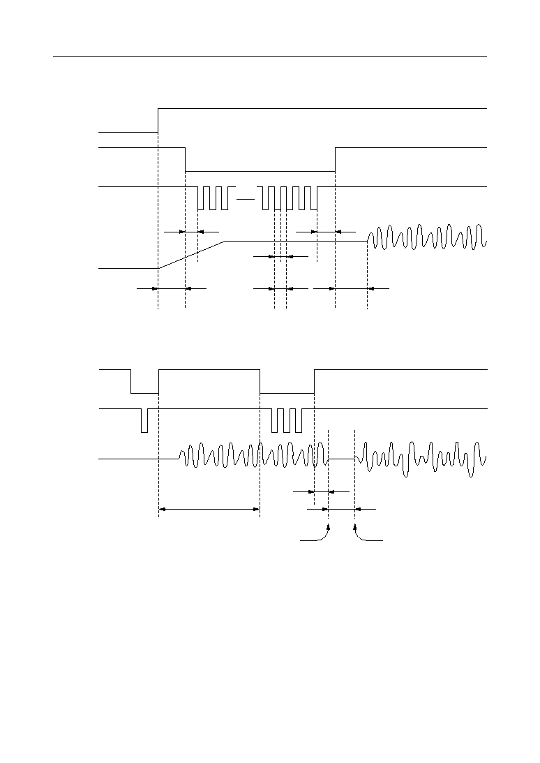
TIMING DIAGRAMS
1. Power-On
t
RST
t
PDH
Reset Power Down
V
DD
PDWN
ST
PI
(I)
(I)
(I)
Note: A level input in combination of PDWN="L", ST="L" and PI="H" resets the LSI.
After Power-On, you need to do an initial reset as shown in the above chart.
2. Activating the LSI and Standby Mode
t
DAR
t
DAF
PDWN
AOUT
(I)
(O)
I
AOUT
1
2
8/22
MSM9831-xxx
° Semiconductor
3. Playback
4. Re-inputting the address while playback is going on
PDWN (I)
ST (I)
PI (I)
AOUT (O)
t
SPS
t
PDSS
t
PW
t
PC
t
SPH
t
SAS
ST (I)
PI (I)
AOUT (O)
t
DPS
t
PP
t
BLN
Current phrase stops
Next phrase starts
9/22
MSM9831-xxx
° Semiconductor
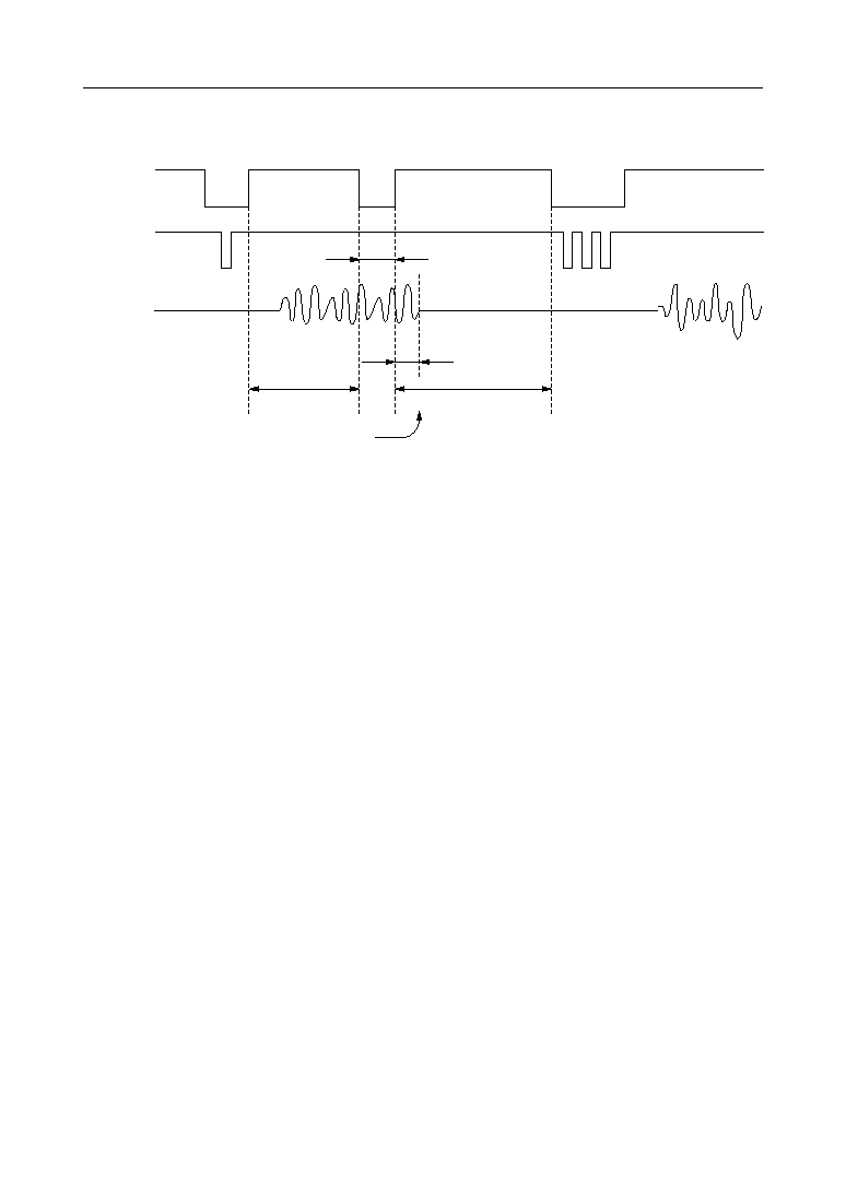
5. Stop Code Input
ST (I)
PI (I)
AOUT (O)
t
DPS
t
PS
Current phrase stops
t
SSW
t
SP
10/22
MSM9831-xxx
° Semiconductor
FUNCTIONAL DESCRIPTION
1. Sampling Frequency
Sampling Frequency can be selected and setup on each phrase address. 7 sampling frequencies
are available for user's choice in preparing Voice Data File at the pre-production stage. Select
sampling frequencies to satisfy f
SAM
=3.9 to 28.0 kHz obtained by frequency dividing ratios in
Table 1.1.
Table 1.1 Sampling Frequency
Sampling Frequency
(f
OSC
=4.096MHz)
Frequency diving ratio
4.0kHz
f
OSC
/1024
5.3kHz
f
OSC
/768
6.4kHz
f
OSC
/640
8.0kHz
f
OSC
/512
10.6kHz
f
OSC
/384
12.8kHz
f
OSC
/320
16.0kHz
f
OSC
/256
2. Recording/Playback Time
Figure 2.1 below shows memory allocation of on-chip 384K bit Mask ROM.
The Mask ROM is partitioned into 4 data areas: user's Area, Phrase Control Table Area, Phrase
Control Area and Test Data Area. Actual memory space is the total Mask ROM capacity (384K
bit) indicated in this document minus 6K bit.
Figure 2.1 Memory Allocation of on-chip Mask ROM (384K bit)
Phrase Control Table Area
Phrase Data Control Area
Test Data Area
User's Area
2K bit
2K bit
2K bit
378K bit

11/22
MSM9831-xxx
° Semiconductor
The playback time is obtained by dividing the memory capacity by the bit rate.
The playback time for 8-bit PCM algorithm is obrained by using the following equation.
Memory capacity [bit]
Bit rate [bps]
Memory capacity [bit]
Sampling frequency [Hz] • 8 [bit]
Playback time [sec] =
=
(384≠6) • 1024 [bit]
8000 [Hz] • 8 [bit]
Playback time =
= 6.0 [sec]
For example, if all phrases are stored in the MSM9802 at 8 kHz sampling frequency, the
maximum playback time is as follows.
3. Playback Method
The MSM9831 uses OKI non-linear PCM algorithm.
In the mid-range of waveform, OKI 8-bit non-linear PCM has precision equivalent to that of 10-
bit straight PCM.
4. Inserting Silence
In addition to normal recorded sound phrases, the MSM9831 allows a user to play back or insert
silence (silent phrase). User can set up time length of silence from a minimum of 32ms to a
maximum of 996ms in 32ms step when f
OSC
=4.096 MHz. These time lengths are directly
proportioned to the clock (f
OSC
) period.
12/22
MSM9831-xxx
° Semiconductor
5. Phrase Control Table
Because the LSI contains the Phrase Control Table, it is possible to play back multiple phrases in
succession by a single easy control operation like controlling a single regular phrase playback.
Up to 8 combined phrases including a silence can be registered in a single address in the Phrase
Control Table.
Further, you can use the maximum memory space for data storage because it is not required to
have the same phrase data.
To show an example, let's assume that your application needs to speak two similar sentences, "It
is fine today" and "It is rainy today." The two sentences have the common words "it", "is" and
"today". What you have to do is to prepare these common sound data, not in sentences but in
words, and to store each combined phrase data in Phrase Control Table as shown in Table 4.1 and
Figure 4.1
Multiple phrases can be played continuously merely by specifying a desired phrase using an X
address. For an example from Table 4.1, when address "01" is specified, "It is fine today" is played,
and when address"02" is specified, "It is rainy" is played.
Phrase Control Table, a silence can be inserted without using the User's Area.
Minimum time for silence
32 ms
Maximum time for silence
992 ms
Time unit for setting up silence
32 ms
Table 4.1 Matrix of the Phrase Control Table
No.
X-Address
(HEX)
Y-Address
(Up to 8 phrases)
Sound Data
1
01
2
02
3
03
30
1E
31
1F
∑ ∑ ∑
∑ ∑ ∑
[04]
Silence
[02]
[01]
[03]
[05]
Silence
[02]
[01]
[03]
[09]
[04]
[02]
[01]
[06] [05] [0A] [03]
∑ ∑ ∑
It is (silence) fine today.
It is (silence) rainy today.
It is fine becoming cloudy, rainy in some areas today.
13/22
MSM9831-xxx
° Semiconductor
Figure 4.1 Phrase Combination Matrix for Phrase Control Table
No. Y-Address
Phrase
1
01
2
02
3
03
5
05
6
06
7
07
8
08
9
09
10
0A
31
1F
--
Phrase Data Registration Area
1
[01]
2
[02]
3
Silence (64ms)
4
[05]
5
[03]
6
--
7
--
8
--
Phrase Control Table Area
Phrase Addigned
n
Silence time length
1
32 ms
2
64 ms
31
992 ms
Setting of silence time
length (32ms
•n)
No. X-Address
1
01
2
02
3
03
4
04
5
05
6
06
7
07
8
08
9
09
31
1F
The silence time lengths are directly
proportional to the clock (f
OSC
) period.
4
04
∑ ∑ ∑ ∑ ∑ ∑ ∑
∑ ∑ ∑ ∑ ∑ ∑ ∑
∑ ∑ ∑
∑ ∑ ∑
∑ ∑ ∑ ∑ ∑ ∑ ∑ ∑ ∑ ∑ ∑ ∑ ∑
∑ ∑ ∑ ∑ ∑ ∑ ∑ ∑ ∑ ∑ ∑ ∑ ∑
∑ ∑ ∑ ∑ ∑ ∑ ∑ ∑ ∑ ∑ ∑ ∑ ∑
it
is
today
rainy
cloudy
snowy
occasionally
becoming
in some areas
fine
it
is
rainy
today

14/22
MSM9831-xxx
° Semiconductor
Figure 5.2 Playback timing when using phrase control data
AOUT (O)
Playback
Phrase 01
Playback
Phrase 02
Playback Phrase 03 Playback Phrase 01
Enter into
Stand-by mode
Reset
Power Down
Current phrase stops
Playback stops
Enter into
Stand-by mode
Power Down
Phrase 01
Selected
Phrase 02
Selected
Phrase 03
Selected
Phrase 01
Selected
Stop Code
PI (I)
ST (I)
PDWN (I)
V
DD
It is fine
today
It is rainy
today
It is fine becoming
cloudy, rainy in
some areas today.
It is fine
today
15/22
MSM9831-xxx
° Semiconductor
6. Oscillation, Clock Signal Input
6-1 Using a Ceramic Oscillator
Figure 6.1 shows an oscillation circuit diagram using a Ceramic Oscillator.
(Select Use a Ceramic Oscillator option on selecting options)
Figure 6.1 Oscillation Circuit with an external ceramic oscillator
The optimal load capacities when connecting ceramic oscillators from MURATA MFG., KYOCERA
CORPORATION, and TDK CORPORATION are shown below for reference.
XT
XT
C1
C2
External capacitor type
MSM9831
XT
XT
Internal capacitor type
MSM9831
Ceramic oscillator
Optimal load
capacity
Supply Voltage
Range (V)
Operating
Temperature
Rnage (∞C)
Maker
Freq (MHz) C
1
(pF) C
2
(pF)
CSA4.00MG
4.0
30
30
3.0 to 5.5
≠40 to +85
MURATA MFG.
Type
CSA4.00MGW
Built in
Built in
CSAC4.00MGC
30
30
CSTCC4.00MG
Built in
Built in
CSA4.00MGU
30
30
CST4.00MGWU
Built in
Built in
CSAC4.00MGCU
30
30
CSTCC4.00MGU
Built in
Built in
2.7 to 5.5
2.6 to 5.5
FCR4.0M5
33
33
FCR4.0MC5
Built in
Built in
2.5 to 5.5
2.5 to 5.5
≠40 to +85
CCR4.0MC3
KBR-4.0MSA
33
33
KBR-4.0MSB
Built in
Built in
2.5 to 5.5
≠20 to +80
KBR-4.0MKC
KBR-4.0MKD
33
33
KBR-4.0MKS
Built in
Built in
PBRC4.00A
33
33
PBRC4.00B
4.0
4.0
TDK
CORPORATION
KYOCERA
CORPORATION

16/22
MSM9831-xxx
° Semiconductor
6-2 Using External Clock Input
Figure 6.2 shows an oscillation circuit diagram using an external clock input.
Figure 6.2 Oscillation Circuit using an external clock input
XT
XT
Open
External Clock, etc. as the timing source
17/22
MSM9831-xxx
° Semiconductor
7. Low-Pass Filter
In this IC, all voice outputs are through the built-in low-pass filter (LPF). Figure 7.1 and Table
7.1 show the LPF frequency characteristics and LPF cutoff frequency respectively.
The frequency characteristics and cutoff frequencies are directly proportional to sampling
frequencies.
Only the voice output through LPF in this IC is enabled.
Figure 7.1 LPF Frequency Characteristics (f
SAM
=8 kHz)
Table 7.1 LPF Cutoff Frequency
0
≠20
≠40
≠60
[dB]
100
1k
10k
≠10
10
≠30
≠50
≠80
≠70
20
[Hz]
10
Sampling Frequency (kHz)
Cutoff Frequency (kHz)
(f
SAM
)
(f
CUT
)
1.2
1.6
4.0
5.3
2.0
6.4
2.5
8.0
3.2
10.6
4.0
12.8
5.0
16.0
18/22
MSM9831-xxx
° Semiconductor
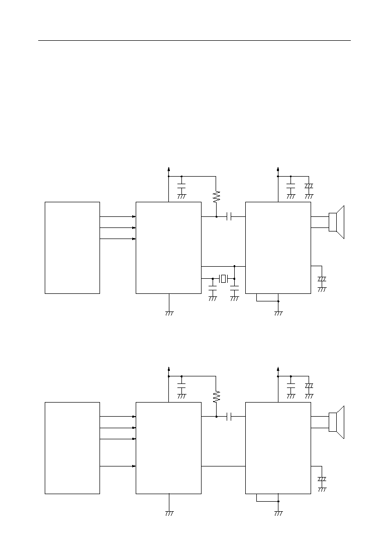
Connecting the MSM9831 to Speaker Driving Amplifier
The MSM9831 uses a current output type D/A converter.
When the MSM9831 is connected to a voltage input type amplifier, it is required to convert the
voice signal that is output as "change of current" into the voice signal that is output as "change
of voltage".
The connection between the MSM9831 and MSC1157 (OKI speaker driving amplifier) when a
resistor is used for the above conversion is described below.
Circuit connection example 1: When V
DD
=5.0V and the amplitude of Ain of the MSC1157
is 2.5V
P-P
P1.2
P1.1
P1.0
ST
PI
PDWN
AOUT
V
DD
+5V
0.1
m
F
500
W
47nF
+5V
0.1
m
F
10
m
F
+
≠
+
≠
4.7
m
F
+
≠
XT
XT
MSM9831
GND
MCU
Ain
V
CC
SP
SP
MSC1157
VR
STBY
GND
SEL
4.096MHz
(Ceramic oscillation is selected)
Circuit connection example 2: When V
DD
=3.0V and the amplitude of Ain of the MSC1157
is 1.5V
P-P
P1.2
P1.1
P1.0
ST
PI
PDWN
AOUT
V
DD
+3V
0.1
m
F
620
W
47nF
+3V
0.1
m
F
10
m
F
+
≠
+
≠
4.7
m
F
+
≠
XT
MSM9831
GND
MCU
Ain
V
CC
SP
SP
MSC1157
VR
STBY
GND
SEL
(External clock input is selected)
CLK
XT
19/22
MSM9831-xxx
° Semiconductor
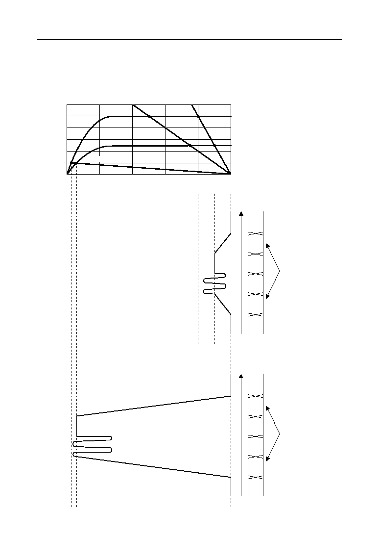
Use a resistor with an appropriate value (R
L
) considering the output voltage (reference the
drawing below).
0
1
2
3
4
5
6
0
1
2
3
4
5
R
L
=500W
R
L
=200W
Maximum output current
Output current at waveform center
VAOUT (V)
IAOUT (mA)
R
L
=5kW
Playback
Standby
Power
down
Power
down
Time
Shift to standby
(2)
Voice waveform is distorted and pop noises
are generated when R
L
=5k
W
* When R
L
is too high
Playback
Standby
Power
down
Power
down
Time
Shift to standby
(1)
Normal voice waveform is obtained
when R
L
=200
W
Relationship between AOUT pin voltage and AOUT output current at V
DD
=5V

20/22
MSM9831-xxx
° Semiconductor
D/A CONVERTER OUTPUT CURRENT
0.0
0.5
1.0
1.5
2.0
2.5
3.0
3.5
4.0
4.5
5.0
5.5
0
1
2
3
4
5
6
Supply voltege (V)
AOUT outptu current (mA)
Relationship between supply voltage and AOUT output current
(Ta=25∞C, VAOUT=V
DD
, PCM at maximum)
≠40
0
1
2
3
4
5
6
Ambient temperature (∞C)
AOUT outptu current (mA)
Relationship between ambient temperature and AOUT output current
(VAOUT=V
DD
, PCM at maximum)
≠20
0
20
40
60
80
100
V
DD
=5V
V
DD
=3V
0.0
0
AOUT pin voltage (V)
AOUT outptu current (mA)
1
2
3
4
5
6
0.5
1.0
1.5
2.0
2.5
3.0
3.5
4.0
4.5
5.0
Relationship between AOUT pin voltage and AOUT output current
(Ta=25∞C, V
DD
=5.0V, PCM at maximum)
21/22
MSM9831-xxx
° Semiconductor
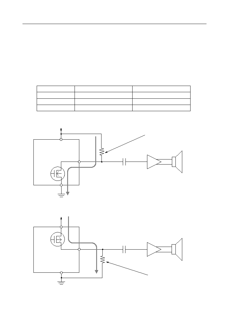
NOTES
1. Internal converter circuit
The MSM9831 has not employed a voltage output type D/A converter but a current output type
D/A converter. Therefore, the voice output circuit of the MSM9831 is different from that of the
MSM6650 family product which has employed a voltage output type D/A converter. The voice
output circuit of the MSM9831 also is different from that of the MSM9800 family product because
the MSM9831 has employed a current flowing-in type D/A converter and the MSM9800 family
product has employed a current flowing-out type D/A converter. (See the table below)
MSM6650 family
MSM9800 family
MSM9831
Product name
D/A converter circuit type
D/A converter output circuit
Voltage output type
--
Current output (flowing-out) type
P-MOS open drain
Current output (flowing-in) type
N-MOS open drain
Circuit connection between the MSM9831 and amplifier IC
V
DD
AOUT
GND
D/A converter
MSM9831
Current flowing direction
AMP
Resistor for conversion from current to voltage
V
DD
AOUT
GND
D/A converter
Current flowing direction
AMP
Resistor for conversion from current to voltage
MSM9800 family
Circuit connection between the MSM9800 family product and amplifier IC
2. Ceramic oscillator
A crystal that is usable in this LSI is described in "Functional Description" of this document. If
you want to use another crystal, it is recommended to evaluate the crystal before using it.
22/22
MSM9831-xxx
° Semiconductor
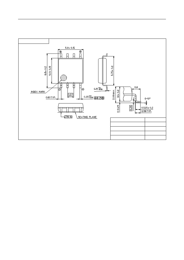
(Unit : mm)
PACKAGE DIMENSIONS
Notes for Mounting the Surface Mount Type Package
The SOP, QFP, TSOP, TQFP, LQFP, SOJ, QFJ (PLCC), SHP, and BGA are surface mount type
packages, which are very susceptible to heat in reflow mounting and humidity absorbed in
storage. Therefore, before you perform reflow mounting, contact Oki's responsible sales person
on the product name, package name, pin number, package code and desired mounting conditions
(reflow method, temperature and times).
SOP8-P-250-1.27-K
Package material
Lead frame material
Pin treatment
Solder plate thickness
Package weight (g)
Epoxy resin
42 alloy
Solder plating
5 mm or more
0.10 TYP.
Mirror finish

NOTICE
1.
The information contained herein can change without notice owing to product and/or
technical improvements. Before using the product, please make sure that the information
being referred to is up-to-date.
2.
The outline of action and examples for application circuits described herein have been
chosen as an explanation for the standard action and performance of the product. When
planning to use the product, please ensure that the external conditions are reflected in the
actual circuit, assembly, and program designs.
3.
When designing your product, please use our product below the specified maximum
ratings and within the specified operating ranges including, but not limited to, operating
voltage, power dissipation, and operating temperature.
4.
Oki assumes no responsibility or liability whatsoever for any failure or unusual or
unexpected operation resulting from misuse, neglect, improper installation, repair, alteration
or accident, improper handling, or unusual physical or electrical stress including, but not
limited to, exposure to parameters beyond the specified maximum ratings or operation
outside the specified operating range.
5.
Neither indemnity against nor license of a third party's industrial and intellectual property
right, etc. is granted by us in connection with the use of the product and/or the information
and drawings contained herein. No responsibility is assumed by us for any infringement
of a third party's right which may result from the use thereof.
6.
The products listed in this document are intended for use in general electronics equipment
for commercial applications (e.g., office automation, communication equipment,
measurement equipment, consumer electronics, etc.). These products are not authorized
for use in any system or application that requires special or enhanced quality and reliability
characteristics nor in any system or application where the failure of such system or
application may result in the loss or damage of property, or death or injury to humans.
Such applications include, but are not limited to, traffic and automotive equipment, safety
devices, aerospace equipment, nuclear power control, medical equipment, and life-support
systems.
7.
Certain products in this document may need government approval before they can be
exported to particular countries. The purchaser assumes the responsibility of determining
the legality of export of these products and will take appropriate and necessary steps at their
own expense for these.
8.
No part of the contents contained herein may be reprinted or reproduced without our prior
permission.
9.
MS-DOS is a registered trademark of Microsoft Corporation.
Copyright 1999 Oki Electric Industry Co., Ltd.
Printed in Japan
E2Y0002-29-62