
OKI Semiconductor
FEDL2250DIGEST-01
Issue Date: Oct. 15, 2002
ML2252/54-XXX, ML22Q54
2-Channel Mixing Oki ADPCM Algorithm-Based Speech Synthesis LSI
1/31
This document contains minimum specifications. For full specifications, please contact your nearest Oki office or
representative.
GENERAL DESCRIPTION
The ML2250 family is a 2-channel mixing speech synthesis device with an on-chip voice data (i.e., phrases)
storing mask ROM and a flash memory. Besides playing the built-in voice data, this device can output voice data
that is input from outside the device. This ML2250 family allows to select the playback method from the 8-bit
PCM, non-linear 8-bit PCM, 16-bit PCM, 2-bit ADPCM2, and 4-bit ADPCM2 algorithms. And the sound volume
is adjustable as well.
The ML2250 family incorporates a 14-bit D/A converter, low-pass filter, and 1-bit DAC (PWM output).
It is easy to configure a speech synthesizer by externally connecting a power amplifier and a CPU to the ML2250
family.
The ML2250 family line-up includes 2 types of products: with on-chip mask ROM, and with on-chip flash
memory.
�
ML2252/54-XXX
This is a CMOS single chip speech synthesis device with an on-chip mask ROM. Products with 2 types of mask
ROMs are available in the ML2250 family depending upon the total playback time length.
�
ML22Q54
The ML22Q54 is a speech synthesis device with a 4-Mbit flash memory built in. The voice data can be easily
written to the flash memory using a special tool. The on-chip flash memory product is suitable for the diversified
low volume production or short delivery time applications that the on-chip mask ROM product cannot support.
The ML22Q54 is most suitable for evaluation because the circuit configuration is the same as the on-chip mask
ROM product.
A combination of fixed and variable messages can be written because it is easy to write to the built-in flash
memory. It is also possible to store and read data, other than voice, to/from an area in the flash memory not used
as voice data.
FEDL2250DIGEST-01
OKI Semiconductor
ML2252/54-XXX, ML22Q54
2/31
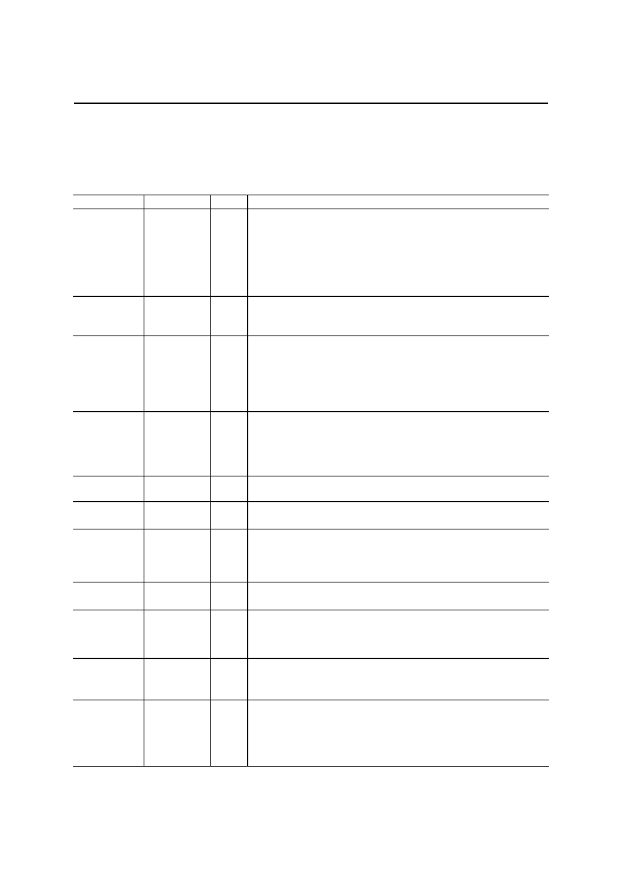
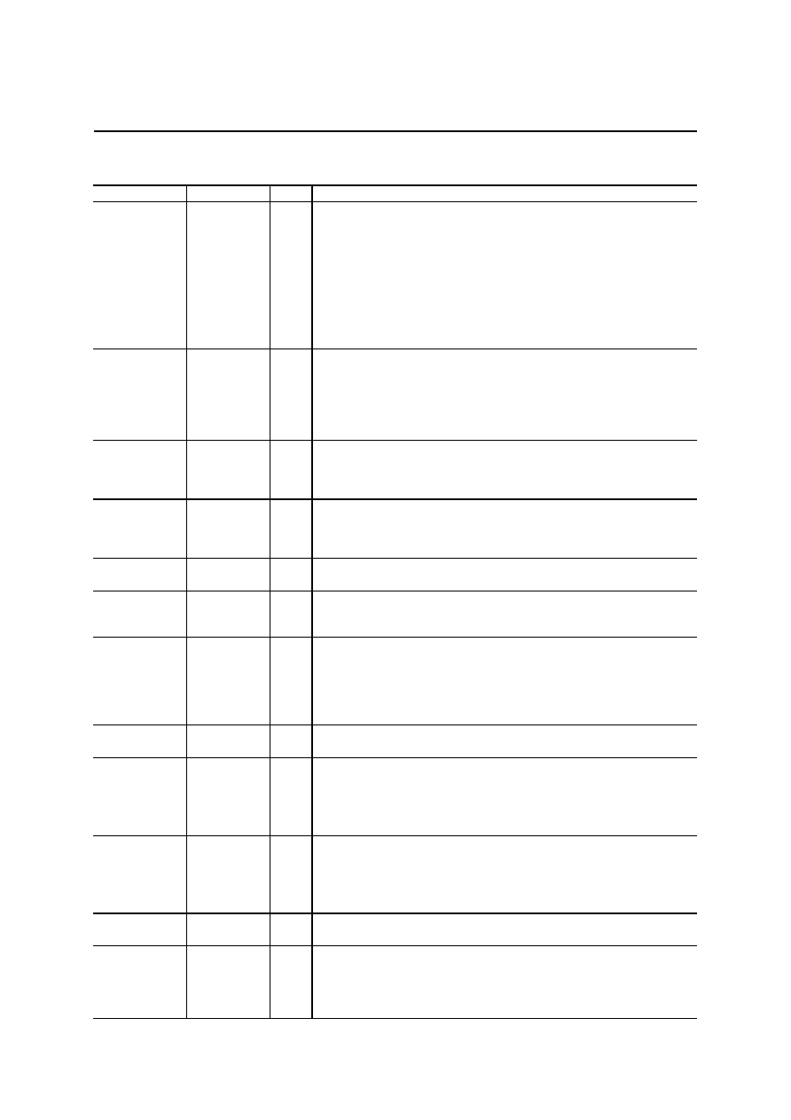
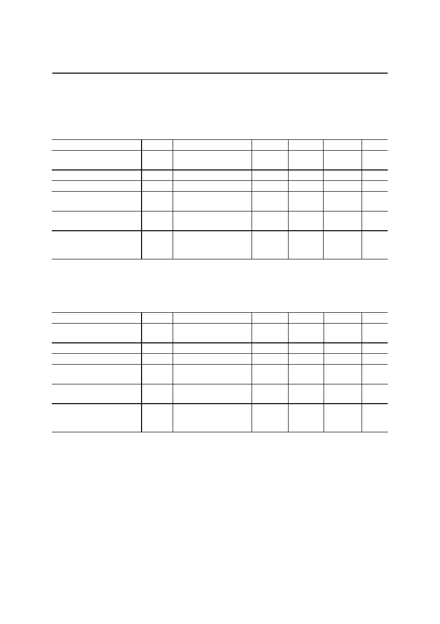
Table below summarizes the points of difference between the ML2250 family and currently manufactured
products with a ROM built in.
ML2250 family
MSM6650 family
MSM9800 family
ML2210 family
Interface
Parallel or serial
Parallel, serial or
stand-alone
Parallel or
stand-alone
Serial
Playback method
2-bit ADPCM2
4-bit ADPCM2
8-bit PCM
8-bit non-linear PCM
16-bit PCM
4-bit ADPCM
8-bit PCM
8-bit PCM
8-bit non-linear PCM
4-bit ADPCM
8-bit PCM
8-bit non-linear PCM
Max. number of
phrases
256 127 63 247
Sampling frequency
(kHz)
4.0/5.3/6.4/8.0/10.7/
12.8/16.0/21.3/25.6/
32.0/42.7/48.0
4.0/5.3/6.4/8.0/10.7/
12.8/16.0/32.0
4.0/5.3/6.4/8.0/10.7/
12.8/16.0
4.0/5.3/6.4/8.0/10.7/
12.8/16.0
Clock frequency
4.096 MHz
256 kHz (CR
oscillation)
4.096 MHz (XT)
256 kHz (CR
oscillation)
4.096 MHz (XT)
4.096 MHz
D/A converter
1-bit DAC PWM
Voltage type: 14 bits
Voltage type: 12 bits Current type: 10 bits Current type: 12 bits
Low-pass filter
FIR type
interpolation filter
Secondary comb
filter
Primary comb filter
Secondary comb
filter
Number of channels 2 channels
2 channels
1 channel
1 channel
Phrase control table
Both 2 channels
without user
definable phrase
restrictions
Can edit 8 phrases
(1 channel only)
Can edit 8 phrases
None
Volume adjustment
29 steps
(�2 dB/�5 dB steps)
4 steps
(�6 dB steps)
Set at VREF.
Set at VREF.
Repeat function
No limit
4 types
None
None
STOP
Each channel
independent
Simultaneous
channels 1 and 2
Available Available
Seam silence
interval in
continuous playback
0 (Note)
4 sampling cycles
3 sampling cycles
4 sampling cycles
Others
External data input
possible
-- -- --
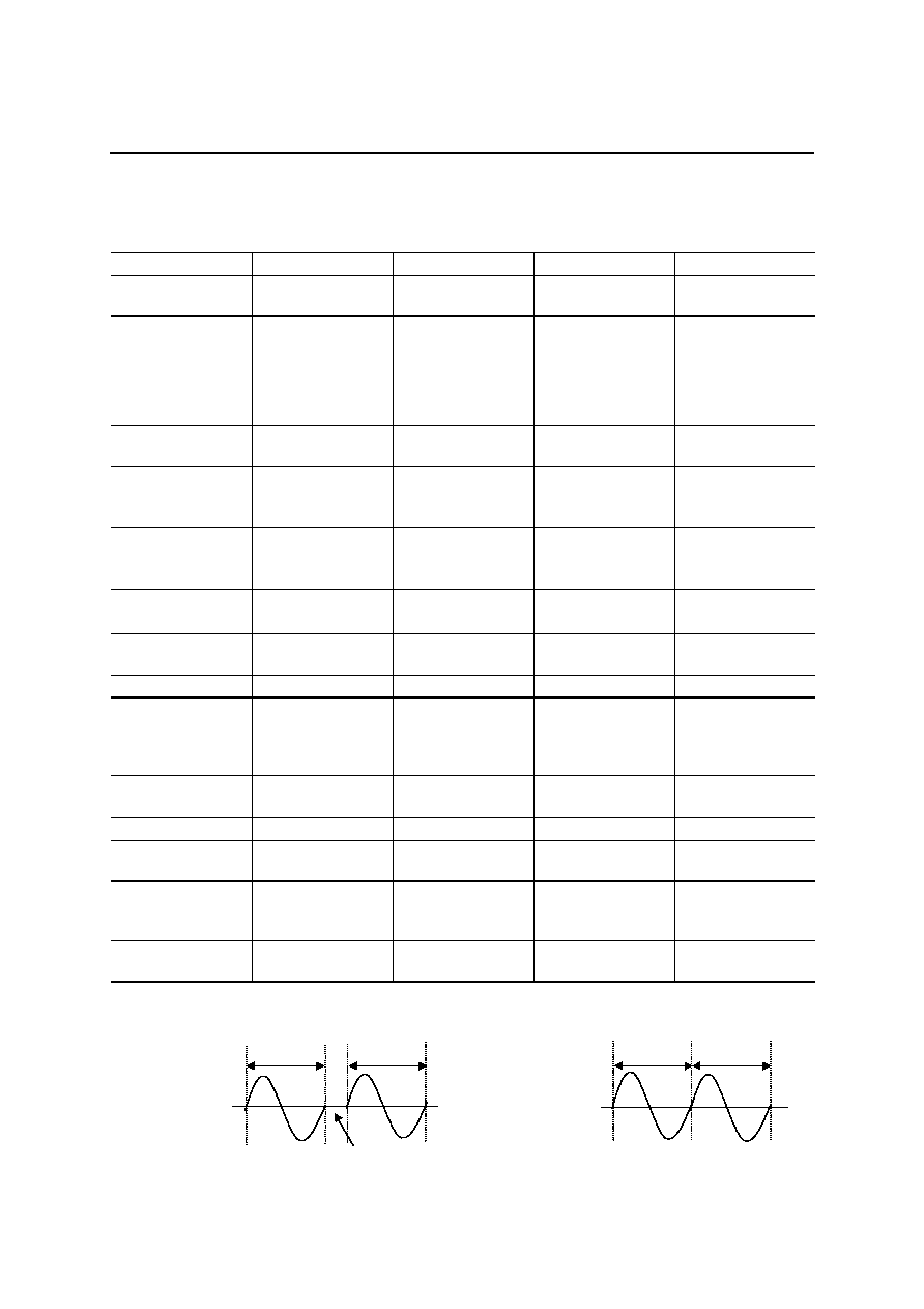
Note: Continuous playback shown in the figure below is possible.
1 phrase
1 phrase
1 phrase
1 phrase
ML2250 family
Conventional
Silence interval
No silence interval

FEDL2250DIGEST-01
OKI Semiconductor
ML2252/54-XXX, ML22Q54
3/31
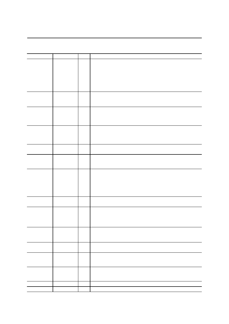
FEATURES
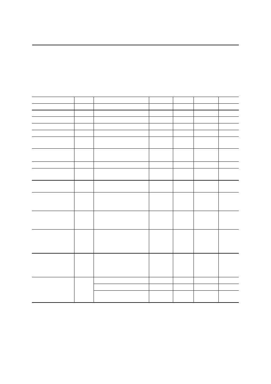
Maximum playback time length (sec) (In 4-bit ADPCM2)
Type ROM
capacity
F
SAM
= 4.0 kHz F
SAM
= 6.4 kHz F
SAM
= 8.0 kHz F
SAM
= 16 kHz F
SAM
= 32 kHz
ML2252 1
Mbit 64.5
40.3 32.2 16.1 8.0
ML2254 4
Mbit 261.1 163.2 130.5 65.2 32.6
ML22Q54 4
Mbit 261.1 163.2 130.5 65.2 32.6
�
Non-linear 8-bit PCM, 8-bit PCM, 16-bit PCM, 2-bit ADPCM2, and 4-bit ADPCM2 algorithms
�
Serial input/parallel input selectable
�
Phrase control table function i.e., user definable phrase control table function
�
2 channels mixing function
�
Master clock frequency:
4.096 MHz
�
Sampling frequency:
4.0 kHz, 5.3 kHz, 6.4 kHz, 8.0 kHz, 10.7 kHz, 12.8 kHz,
16.0 kHz, 21.3 kHz, 25.6 kHz, 32.0 kHz, 42.7 kHz, 48 kHz
�
Maximum number of phrases:
256 phrases
�
Sound volume adjustment function built in (2 sounds independently adjustable in 29 steps)
�
External voice data can be input
�
1-bit D/A converter, and14-bit D/A converter built in
�
Built-in low-pass filter:
Digital filter
�
Package:
44-pin plastic QFP (QFP44-P-910-0.80-2K)
(ML2252-XXXGA/ML2254-XXXGA/ML22Q54GA-MC)
FEDL2250DIGEST-01
OK
I Sem
i
cond
uct
o
r
ML2
2
52/
54
-
XXX,
ML2
2
Q
5
4
4/
3
1
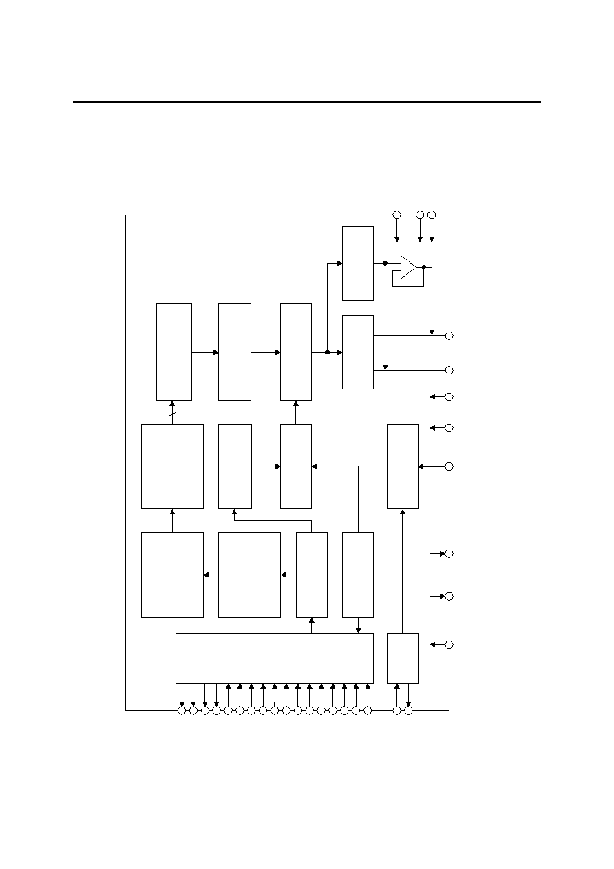
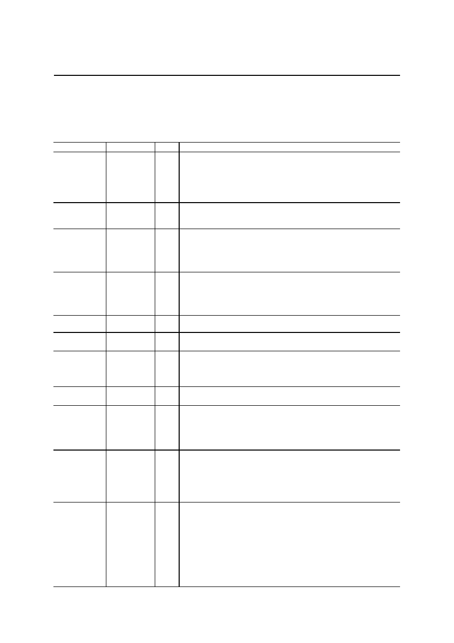
BLOCK D
I
AGR
A
M
ML2
252
/54
-
XX
X
XT
XT
TESTO2
OSC
CPU
Interface
16bit(ML2252)
18bit(ML2254)
Multiplexer
2bit ADPCM2
/4bit ADPCM2
Synthesizer
Digital Filter
1bit DAC
8bit PCM
16bit PCM
Synthesizer & 2ch Mix
Timing Controller
TESTO1 DV
DD
DGND
OUT(�)
/AOUT
RESET
16
TEST
16bit(ML2252)
18bit(ML2254)
Address Controller
Command Register
Phrase Address
Register
1Mbit(ML2252)
4Mbit(ML2254)
ROM
Phrase Control
Table
Loop Volume
OUT(+)
/DAO
NCR1/NDR
NCR2/
DL
BUSY1
BUSY2
/
ERR
SERIAL
D7/DI
D6/SCK
D5/DO
D4
D3
D2
D1
D0
WR
CS
DW
RD
14bit DAC
OPTANA
AV
DD
AGND
FEDL2250DIGEST-01
OK
I Sem
i
cond
uct
o
r
ML2
2
52/
54
-
XXX,
ML2
2
Q
5
4
5/
3
1
M
L
22
Q
54
XT
XT
OSC
CPU
Interface
18bit Multiplexer
2bit ADPCM2
/4bit ADPCM2
Synthesizer
Digital Filter
1bit DAC
8bit PCM
16bit PCM
Synthesizer & 2ch Mix
OUT(�)
/AOUT
16
Timing Controller
RESET
18bit
Address Controller
Command
Controller
4Mbit Flash
ROM
Phrase Control
Table
Loop Volume
DV
DD
DGND
OUT(+)
/DAO
NCR1/NDR
NCR2/
DL
BUSY1
BUSY2
/
ERR
SERIAL
D7/DI
D6/SCK
D5/DO
D4
D3
D2
D1
D0
WR
CS
DW
RD
RD/
BY
14bit DAC
OPTANA
AV
DD
AGND
TEST
TESTO
FEDL2250DIGEST-01
OKI Semiconductor
ML2252/54-XXX, ML22Q54
6/31
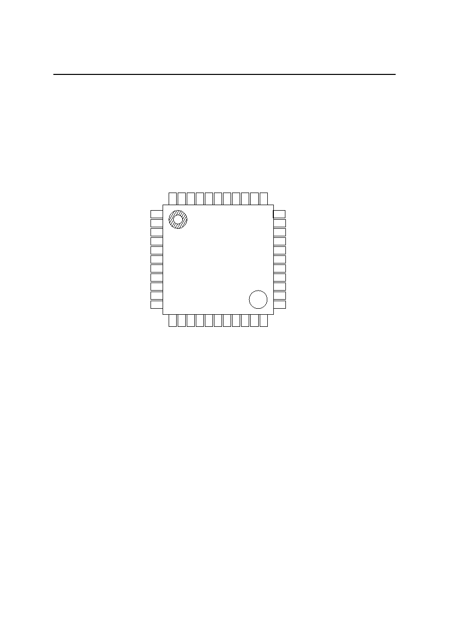
PIN CONFIGURATION (TOP VIEW)
ML2252/54-XXX
44-pin plastic QFP
44
43
42
41
40
39
38
37
36
35
34
NC: No Connection
NC
DV
DD
XT
X
T
D0
DGN
D
D1
D2
D3
D4
NC
NC
DW
BUSY1
NCR2/
DL
NCR1/NDR
RD
TESTO1
TESTO2
RESET
TEST
NC
1
2
3
4
5
6
7
8
9
10
11
NC
SERIAL
DGND
AV
DD
OUT(�)/AOUT
OUT(+)/DAO
AGND
D7/DI
NC
D6/SCK
D5/DO
33
32
31
30
29
28
27
26
25
24
23
12
13
14
15
16
17
18
19
20
21
22
NC
B
USY
2
/
ERR
W
R
NC
DV
DD
DGND
NC
OP
T
A
NA
C
S
NC
NC
FEDL2250DIGEST-01
OKI Semiconductor
ML2252/54-XXX, ML22Q54
7/31
ML22Q54
44-pin plastic QFP
NC: No Connection
NC
DV
DD
XT
X
T
D0
DG
N
D
D1
D2
D3
D4
NC
NC
DW
BUSY1
NCR2/
DL
NCR1/NDR
RD
TESTO
RD/
BY
RESET
TEST
NC
1
2
3
4
5
6
7
8
9
10
11
NC
SERIAL
DGND
AV
DD
OUT(�)/AOUT
OUT(+)/DAO
AGND
D7/DI
NC
D6/SCK
D5/DO
33
32
31
30
29
28
27
26
25
24
23
12
13
14
15
16
17
18
19
20
21
22
NC
B
USY2
/
ER
R
W
R
NC
DV
DD
DGND
NC
OP
T
A
N
A
C
S
NC
NC
44
43
42
41
40
39
38
37
36
35
34
FEDL2250DIGEST-01
OKI Semiconductor
ML2252/54-XXX, ML22Q54
8/31
PIN DESCRIPTIONS-1
ML2252/54-XXX Common Pins
44-pin plastic QFP
Pin Symbol
Type
Description
43
BUSY2
/
ERR
O
When using the built-in ROM for voice output, this pin outputs "L" level
while channel 2 side processes a command and while plays back
voice.
Works as
ERR
pin when using the EXT command for voice output. If an
abnormality occurred in the transfer of data, the pin will output "L" level
and the voice output may become noisy.
"H" level at power on.
3
BUSY1
O
Outputs "L" level while the channel 1 side processes a command and
plays back voice.
"H" level at power on.
4 NCR2/
DL
O
The command input of channel 2 side is valid at "H" level when using
the built-in ROM for voice output.
Works as
DL
pin when using EXT command for the voice output. This
pin outputs the signal that captures voice data to inside. The data is
captured inside on the rising edge of
DL
.
"H" level at power on.
5 NCR1/NDR
O
The command input of channel 1 side is valid at "H" level when using
the built-in ROM for voice output.
Works as NDR pin when using EXT command for the voice output. The
voice data input is valid at "H" level.
"H" level at power on.
9
RESET
I
At "L" level input, the device enters the initial state; the oscillation stops,
and AOUT output and DAQ output are GND level at this time.
10 TEST
I
Test pin for the device.
Input "L" level to this pin. This pin has a pull-down resistor built in.
14 XT
I
Wired to a crystal or ceramic oscillator.
A feedback resistor of around 1 M
is built in between this XT pin and
XT
pin (pin 15).
When using an external clock, input the clock from this pin.
15
XT
O
Wired to a ceramic or crystal oscillator.
When using an external clock, keep this pin open.
16, 18, 19, 20
D3
D2
D1
D0
I/O
CPU interface data bus pins in the parallel input interface.
Channel status output pins at
RD
pin = "L" level.
In the serial input interface, keep these pins at "L" level.
21 D4
I/O
CPU interface data bus pin in the parallel input interface.
When
RD
pin is at "L" level, this pin D4 usually outputs "L" level.
In the serial input interface, keep this pin at "L" level.
23 D5/DO
I/O
CPU interface data bus pin in the parallel input interface.
When
RD
pin is at "L" level, this D5/DO pin usually outputs "L" level.
Works as channel status output pin in the serial interface.
When
CS
and
RD
pins are "L" level, the status of each channel is output
serially from this D5/DO pin in synchronization with SCK clock.
FEDL2250DIGEST-01
OKI Semiconductor
ML2252/54-XXX, ML22Q54
9/31
Pin Symbol
Type
Description
24 D6/SCK
I/O
CPU interface data bus pin in the parallel input interface.
Usually outputs "L" level when
RD
= "L" level.
Works as serial clock input pin in the serial input interface.
When the SCK input is at "L" level on the falling edge of
CS
, the DI input
is captured in the device on the rising edge of SCK clock. And when the
SCK input is at "H" level on the falling edge of
CS
, the DI input is
captured on the falling edge of SCK clock.
26 D7/DI
I/O
CPU interface data bus pin in the parallel input interface.
Usually output "L" level when
RD
is at "L" level.
Works as serial data input pin in the serial input interface.
28 OUT(+)/DAO
O
When OPTANA pin is at "H" level, this OUT(+)/DAO pin outputs PWM
(positive phase) of 1-bit DAC.
When OPTANA pin is at "L" level, the OUT(+)/DAO pin outputs analog
signal of 14-bit DAC.
29 OUT(�)/AOUT
O
When OPTANA pin is at "H" level, this OUT(�)/AOUT pin outputs PWM
(reverse phase) of 1-bit DAC.
When OPTANA pin is at "L" level, the OUT(�)/AOUT pin usually outputs
the analog signal of 14-bit DAC via voltage follower.
32 SERIAL
I
CPU interface switching pin.
Serial input interface at "H" level. And parallel input interface at "L" level.
36
CS
I
CPU interface chip select pin.
When
CS
pin is at "H" level, the
WR
,
DW
, and
RD
signals cannot be
input to the device.
37 OPTANA
I
Analog output/PWM output select signal.
When OPTANA pin is at "H" level, the PWM of 1-bit DAC outputs from
OUT(+)/DAO and OUT(�)/AOUT pins.
When OPTANA pin is at "L" level, the analog signal of 14-bit DAC is
output from OUT(+)/DAO pin and from OUT(�)/AOUT pin via voltage
follower.
42
WR
I
CPU interface write signal.
When
CS
pin is at "H" level, the
WR
signal cannot be input to the device.
2
DW
I
Data write signal when using EXT command for the voice output.
Set the pin to "H" level when not using EXT command.
When
CS
pin is at "H" level, the
DW
signal cannot be input to the device.
This pin has a pull-up resistor built in.
6
RD
I
CPU interface read signal.
When
CS
pin is at "H" level, the
RD
signal cannot be input to the device.
This pin has a pull-up resistor built in.
7, 8
TESTO1
TESTO2
O
Output pin for testing.
Keep this pin open.
30 AV
DD
--
Analog power supply pin.
Insert a 0.1
�
F or larger bypass capacitor between this pin and AGND
pin.
13, 40
DV
DD
--
Digital power supply pin.
Insert a 0.1
�
F or larger
bypass capacitor between this pin and DGND
pin.
27
AGND
--
Analog ground pin.
17, 31, 39
DGND
--
Digital ground pin.
FEDL2250DIGEST-01
OKI Semiconductor
ML2252/54-XXX, ML22Q54
10/31
PIN DESCRIPTIONS-2
ML22Q54 Pins
44-pin plastic QFP
Pin Symbol
Type
Description
43
BUSY2
/
ERR
O
When using the built-in ROM for voice output, this pin outputs "L" level
while channel 2 side processes a command and while plays back voice.
Works as
ERR
pin when using EXT command for the voice output. If an
abnormality occurred in the transfer of data, the
ERR
pin outputs "L"
level and the voice output may become noisy.
"H" level at power on.
3
BUSY1
O
Outputs "L" level while the channel 1 side processes a command and
while plays back voice.
"H" level at power on.
4 NCR2/
DL
O
The input command of channel 2 is valid at "H" level when using the
built-in ROM for voice output.
DL
pin when using EXT command for the voice output. It outputs the
voice data capture signal. The data is captured on the rising edge of
DL
.
"H" level at power on.
5 NCR1/NDR
O
The command input of channel 1 side is valid at "H" level when using
the built-in ROM for voice output.
NDR pin when using EXT command for the voice output. The voice data
input is effective at "H" level.
"H" level at power on.
9
RESET
I
When "L" level is input to this pin, the device is reset, the oscillation
stops, and AOUT and DAQ outputs go into GND level.
10 TEST
I
Test pin for the device.
Input "L" level to this pin. This pin has a pull-down resistor built in.
14 XT
I
Wired to a crystal or ceramic oscillator.
A feedback resistor of around 1 M
is built in between this XT pin and
XT
pin (pin 15).
When using an external clock, input the clock from this pin.
15
XT
O
Wired to a ceramic or crystal oscillator.
When using an external clock, keep this pin open.
16, 18, 19, 20
D3
D2
D1
D0
I/O
CPU interface data bus pins in the parallel input interface.
Channel status output pins when
RD
is at "L" level.
The pins output the flash memory data when reading the built-in flash
memory data.
In the serial input interface, keep these pins at "L" level.
21 D4
I/O
CPU interface data bus pin in the parallel input interface.
The pin outputs flash memory data when reading the built-in flash
memory data.
When
RD
is at "L" level other than when reading the flash memory data,
this pin usually outputs "L" level.
In the serial input interface, keep this pin at "L" level.
23 D5/DO
I/O
CPU interface data bus pin in the parallel input interface.
The pin outputs flash memory data when reading the built-in flash
memory data.
When
RD
is at "L" level other than when reading the flash memory data,
this pin usually outputs "L" level.
Channel status output pin in the serial input interface.
When
CS
and
RD
are at "L" level, this D5/DO pin serially outputs the
status of each channel in synchronization with SCK clock. When
reading data of the built-in flash memory, the pin will output serially the
flash memory data.
FEDL2250DIGEST-01
OKI Semiconductor
ML2252/54-XXX, ML22Q54
11/31
Pin Symbol
Type
Description
24 D6/SCK
I/O
Works as CPU interface data bus pin in parallel input interface.
Works as flash memory data output pin when reading the built-in flash
memory data.
When
RD
is at "L" level other than when reading the flash memory data,
this D6/SCK pin usually outputs "L" level.
Works as serial clock input pin in the serial input interface.
When the SCK input is at "L" level on the falling edge of
CS
, the DI input
is captured in device on the rising edge of SCK clock. And when the
SCK input is at "H" level on the falling edge of
CS
, the DI input is
captured on the falling edge of SCK clock.
26 D7/DI
I/O
Works as CPU interface data bus pin in the parallel input interface.
Works as flash data output pin when reading the built-in flash memory
data.
When
RD
is at "L" level at times other than reading the flash memory
data, this D7/DI pin usually outputs "L" level.
Works as serial data input pin in the serial input interface.
28 OUT(+)/DAO
O
When OPTANA pin is at "H" level, this OUT(+)/DAO pin outputs PWM
(positive phase) of 1-bit DAC.
And when OPTANA pin is at "L" level, the OUT(+)/DAO pin outputs the
14-bit DAC analog signal.
29 OUT(�)/AOUT
O
When OPTANA pin is at "H" level, this OUT(�)/AOUT pin outputs PWM
(reverse phase) of 1-bit DAC.
And when OPTANA pin is at "L" level, the OUT(�)/AOUT pin outputs the
14-bit DAC analog signal via voltage follower.
32 SERIAL
I
CPU interface switching pin.
At "H" level: Serial input interface. At "L" level: Parallel input interface.
36
CS
I
CPU interface chip select pin.
When
CS
pin is at "H" level, the
WR
,
DW
, and
RD
signals cannot be
input to the device.
37 OPTANA
I
Analog output/PWM output select signal.
At OPTANA pin = "H" level, PWM of 1-bit DAC is output from
OUT(+)/DAO and OUT(�)/AOUT pins.
At OPTANA pin = "L" level, 14-bit DAC analog signal is output from
OUT(+)/DAO pin and 14-bit DAC analog signal is output from
OUT(�)/AOUT pin via the voltage follower.
42
WR
I
CPU interface write signal.
When
CS
pin is at "H" level, the
WR
signal cannot be input to the device.
2
DW
I
Data write signal at EXT command and Flash I/F command.
When the EXT and Flash I/F commands are not used, keep this pin at
"H" level.
When
CS
pin is at "H" level, the
DW
signal cannot be input to the device.
This pin has a pull-up resistor built in.
6
RD
I
CPU interface read signal.
This pin is used when reading the status signal of each channel or when
reading data of the built-in flash memory.
When not in use, keep this pin to "H" level.
This pin has a pull-up resistor built in.
7 TESTO
O
Output pin for testing.
Keep this pin open.
8 RD/BY
O
Output pin to indicate the automatic erase/write status of the built-in
flash memory.
Outputs "L" level during erase or programming cycle to indicate the
busy state. Goes to "H" level at the end of the erase or programming
cycle and enters into the ready state.
FEDL2250DIGEST-01
OKI Semiconductor
ML2252/54-XXX, ML22Q54
12/31
Pin Symbol
Type
Description
30 AV
DD
--
Analog power supply pin.
Insert a 0.1
�
F or larger bypass capacitor between this pin and AGND
pin.
13, 40
DV
DD
--
Digital power supply pin.
Insert a 0.1
�
F or larger bypass capacitor between this pin and DGND
pin.
27
AGND
--
Analog ground pin.
17, 31, 39
DGND
--
Digital ground pin.

FEDL2250DIGEST-01
OKI Semiconductor
ML2252/54-XXX, ML22Q54
13/31
ABSOLUTE MAXIMUM RATINGS
(GND = 0 V)
Parameter Symbol Condition
Rating
Unit
Power supply voltage
V
DD
�0.3 to +7.0
V
Input voltage
V
IN
Ta = 25�C
�0.3 to V
DD
+0.3
V
Storage temperature
T
STG
--
�55 to +150
�C
RECOMMENDED OPERATING CONDITIONS (3 V)
ML2252/54-XXX, ML22Q54
(GND = 0 V)
Parameter Symbol Condition
Range
Unit
Power supply voltage
V
DD
--
2.7 to 3.6
V
ML2252/54-XXX
�40 to +85
Operating temperature
T
OP
ML22Q54
0 to +70
�C
Min. Typ. Max.
Master clock frequency
f
OSC
--
3.5 4.096 4.5
MHz
RECOMMENDED OPERATING CONDITIONS (5 V)
ML2252/54-XXX
(GND = 0 V)
Parameter Symbol Condition
Range
Unit
Power supply voltage
V
DD
--
4.5 to 5.5
V
Operating temperature
T
OP
--
�40 to +85
�C
Min. Typ. Max.
Master clock frequency
f
OSC
--
3.5 4.096 4.5
MHz
FEDL2250DIGEST-01
OKI Semiconductor
ML2252/54-XXX, ML22Q54
14/31
ELECTRICAL CHARACTERISTICS
DC Characteristics (3 V)
ML2252/54-XXX, ML22Q54
ML2252/54-XXX: DV
DD
= AV
DD
= 2.7 to 3.6 V, DGND = AGND = 0 V, Ta = �40 to +85�C
ML22Q54: DV
DD
= AV
DD
= 2.7 to 3.6 V, DGND = AGND = 0 V, Ta = 0 to +70�C
Parameter Symbol
Condition
Min. Typ. Max. Unit
"H" input voltage
V
IH
--
0.86
�
V
DD
-- -- V
"L" input voltage
V
IL
-- --
--
0.14
�
V
DD
V
"H" output voltage
V
OH
I
OH
= �1 mA
V
DD
�0.4
--
--
V
"L" output voltage
V
OL
I
OL
= 2 mA
--
--
0.4
V
"H" input current 1
I
IH1
V
IH
= V
DD
--
--
10
�
A
"H" input current 2
(Note 1)
I
IH2
V
IH
= V
DD
0.3
2.0
15
�
A
"H" input current 3
(Note 2)
I
IH3
V
IH
= V
DD
Pull-down resistor built in pin
8 40 130
�
A
"L" input current 1
I
IL1
V
IL
= GND
�10
--
--
�
A
"L" input current 2
(Note 3)
I
IL2
V
IL
= GND
Pull-up resistor built in pin
�120 �40 �10
�
A
"L" input current 3
(Note 1)
I
IL3
V
IL
= GND
�15
�2.0
�0.3
�
A
Playback
Operating current
consumption 1
I
DD1
f
OSC
= 4.096 MHz at no load
OPTANA = "L"
-- 9 35 mA
Playback
Operating current
consumption 2
I
DD2
f
OSC
= 4.096 MHz at no load
OPTANA = "H"
-- 10 35 mA
Buit-in Flash
memory access
Operating current
consumption 1
I
DD2
f
OSC
= 4.096 MHz at no load
Read Operation
(ML22Q54)
-- 10 35 mA
Buit-in Flash
memory access
Operating current
consumption 2
I
DD2
f
OSC
= 4.096 MHz at no load
Write and Erase Operation
(ML22Q54)
-- 20 60 mA
Ta = �40 to +70�C
--
--
15
�
A
Ta = �40 to +85�C
--
--
50
�
A
Standby current
consumption
I
DDS
Ta = 0 to +70�C
(ML22Q54)
-- -- 55
�
A
Notes: 1. Applies to XT pin.
2. Applies to TEST pin.
3.
Applies
to
RD
and
DW
pins.
FEDL2250DIGEST-01
OKI Semiconductor
ML2252/54-XXX, ML22Q54
15/31
DC Characteristics (5 V)
ML2252/54-XXX
DV
DD
= AV
DD
= 4.5 to 5.5 V, DGND = AGND = 0 V, Ta = �40 to +85�C
Parameter Symbol
Condition
Min. Typ. Max. Unit
"H" input voltage
V
IH
--
0.8
�
V
DD
--
--
V
"L" input voltage
V
IL
-- --
--
0.2
�
V
DD
V
"H" output voltage
V
OH
I
OH
= �1 mA
V
DD
�0.4
--
--
V
"L" output voltage
V
OL
I
OL
= 2 mA
--
--
0.4
V
"H" input current 1
I
IH1
V
IH
= V
DD
--
--
10
�
A
"H" input current 2
(Note 1)
I
IH2
V
IH
= V
DD
0.8
5.0
20
�
A
"H" input current 3
(Note 2)
I
IH3
V
IH
= V
DD
Pull-down resistor built in pin
30 -- 350
�
A
"L" input current 1
I
IL1
V
IL
= GND
�10
--
--
�
A
"L" input current 2
(Note 3)
I
IL2
V
IL
= GND
Pull-up resistor built in pin
�230 -- �60
�
A
"L" input current 3
(Note 1)
I
IL3
V
IL
= GND
�20
�5.0
�0.8
�
A
Operating current
consumption 1
I
DD1
f
OSC
= 4.096 MHz at no load
OPTANA = "L"
-- 19 40
mA
Operating current
consumption 2
I
DD2
f
OSC
= 4.096 MHz at no load
OPTANA = "H"
-- 23 40
mA
Ta = �40 to +70�C
--
--
15
�
A
Standby current
consumption
I
DDS
Ta = �40 to +85�C
--
--
100
�
A
Notes: 1. Applies to XT pin.
2. Applies to TEST pin.
3.
Applies
to
RD
and
DW
pins.
FEDL2250DIGEST-01
OKI Semiconductor
ML2252/54-XXX, ML22Q54
16/31
Analog Section Characteristics (3 V)
ML2252/54-XXX, ML22Q54
ML2252/54-XXX: DV
DD
= AV
DD
= 2.7 to 3.6 V, DGND = AGND = 0 V, Ta = �40 to +85�C
ML22Q54: DV
DD
= AV
DD
= 2.7 to 3.6 V, DGND = AGND = 0 V, Ta = 0 to +70�C
Parameter Symbol
Condition Min.
Typ.
Max.
Unit
AOUT output load
resistance
R
LAO
-- 50
--
--
k
AOUT output voltage range
V
AOUT
No output load
0.5
--
AV
DD
�0.5
V
DAO output impedance
R
DAO
-- 30
43
60
k
OUT(+), OUT(�) "H" level
output voltage
V
PWMH
I
OH
= �2 mA
AV
DD
�0.4
--
--
V
OUT(+), OUT(�) "L" level
output voltage
V
PWML
I
OH
= 2 mA
--
--
0.4
V
Analog output maximum
amplitude when PWM
output is selected.
V
PWMO
20 kHz LPF used when
OPTANA pin = "H".
-- --
AV
DD
�
0.5
V
P-P
Analog Section Characteristics (5 V)
ML2252/54-XXX
DV
DD
= AV
DD
= 4.5 to 5.5 V, DGND = AGND = 0 V, Ta = �40 to +85�C
Parameter Symbol
Condition Min.
Typ.
Max.
Unit
AOUT output load
resistance
R
LAO
-- 50
--
--
k
AOUT output voltage range
V
AOUT
No output load
0.5
--
AV
DD
�0.5
V
DAO output impedance
R
DAO
-- 30
43
60
k
OUT(+), OUT(�) "H" level
output voltage
V
PWMH
I
OH
= �2 mA
AV
DD
�0.4
--
--
V
OUT(+), OUT(�) "L" level
output voltage
V
PWML
I
OH
= 2 mA
--
--
0.4
V
Analog output maximum
amplitude when PWM
output is selected.
V
PWMO
20 kHz LPF used when
OPTANA pin = "H".
-- --
AV
DD
�
0.5
V
P-P
FEDL2250DIGEST-01
OKI Semiconductor
ML2252/54-XXX, ML22Q54
17/31
FUNCTIONAL DESCRIPTION
Micro-computer Interface
The micro-computer interface in the ML2250 family has 2 types of interface circuits built in: Parallel interface and
serial interface. The interface setting can be changed with the SERIAL pin.
SERIAL pin = "H" level: Serial interface
SERIAL pin = "L" level: Parallel interface
Table below shows the SERIAL pin status in the serial and parallel interfaces.
SERIAL = "L"
SERIAL = "H"
Parallel interface
Serial interface
D7 (I/O)
D (I)
Serial data input pin
D6 (I/O)
SCK (I)
Serial clock input pin
D5 (I/O)
DO (O)
Serial data output pin
D4 (I/O)
D4 (I)
Not used. (Input "L" level.)
D3 (I/O)
D3 (I)
Not used. (Input "L" level.)
D2 (I/O)
D2 (I)
Not used. (Input "L" level.)
D1 (I/O)
D1 (I)
Not used. (Input "L" level.)
D0 (I/O)
Data input/output pins
D0 (I)
Not used. (Input "L" level.)
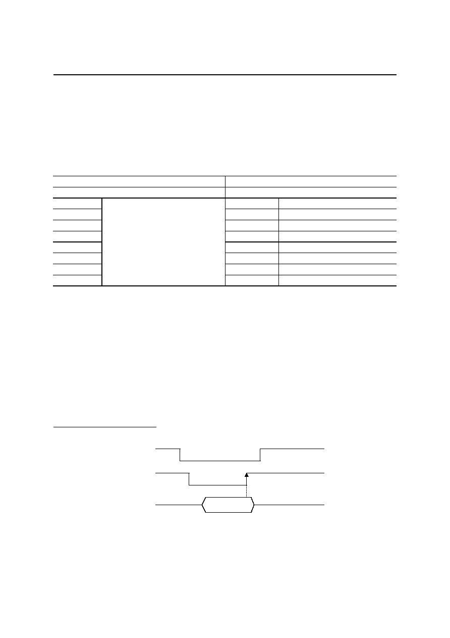
1. Parallel Interface
When selecting the parallel interface, the I/O pins
CS, WR, DW, D7 to D0, and RD are used as input pins to
input various commands and data, and as output pins to read out the status of the commands and data input.
The micro-computer interface becomes effective when the
CS pin is set to "L" level.
When a command or data is input, the input data to D7 through D0 pins is captured inside the device on the
rising edge of the
WR pin.
The
DW pin is used to input data after having input the EXT or Flash I/F command. The method to input data
to the
DW pin is the same as the method to input command from the WR pin.
To read the channels status, pins
CS and RD are made "L" level. By doing so, the status signals (NCR1, NCR2,
BUSY1, BUSY2) of each channel are output to D3 through D0 pins. D7 to D4 pins usually output "L" level.
Command and Data Input Timing
CS
(I)
WR
,
DW
(I)
D7 to D0 (I/O)
Data Stable
FEDL2250DIGEST-01
OKI Semiconductor
ML2252/54-XXX, ML22Q54
18/31
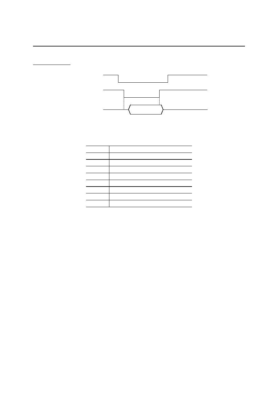
Status Read Timing
Table below shows the contents of each data output when reading the status of the channels.
Pin
Output status signal
D7 "L"
level
D6 "L"
level
D5 "L"
level
D4 "L"
level
D3
Channel 2 busy output (
BUSY2
)
D2
Channel 1 busy output (
BUSY1
)
D1
Channel 2 NCR output (NCR2)
D0
Channel 1 NCR output (NCR1)
The
BUSY signal outputs "L" level when either a command is being processed or the playback of a pertinent
channel is going on. In other states, the
BUSY signal outputs "H" level.
The NCR signal outputs "L" level when either a command is being processed or a pertinent channel is in standby
for playback. In other states, the NCR signal outputs "H" level.
CS
(I)
RD
(I)
D7 to D0 (I/O)
Data Stable

FEDL2250DIGEST-01
OKI Semiconductor
ML2252/54-XXX, ML22Q54
19/31
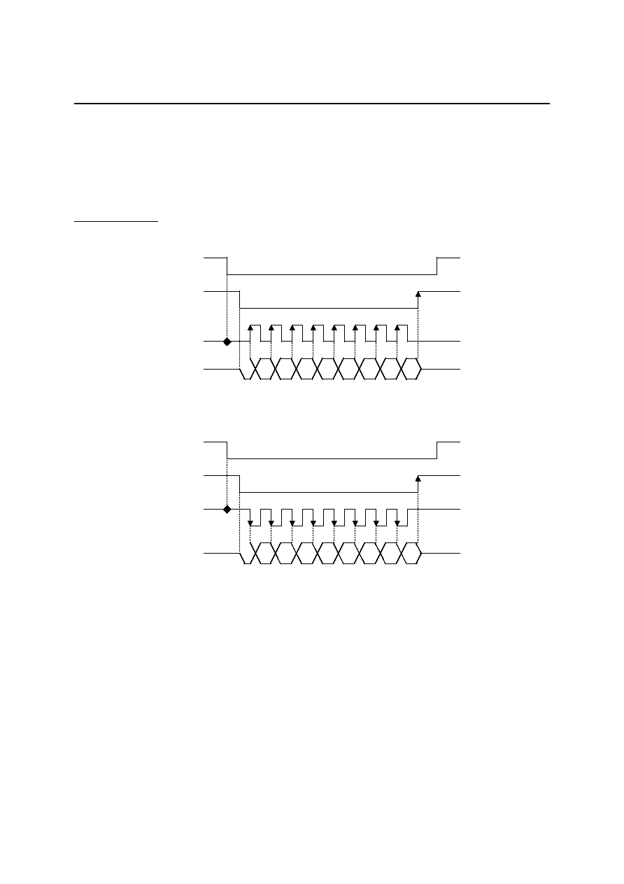
2. Serial Interface
When selecting the serial interface, the I/O pins
CS, WR, DW, DI, SCK, RD, and DO are used as input pins to
input various commands and data, and as output pins to read out the status of the commands and data.
The micro-computer interface becomes effective when
CS pin is set to "L" level.
To input the commands and data, "L" level is input to
CS and WR pins followed by, from MSB, to DI pin in
synchronization with the input clock signal at SCK pin. Data at DI pin is captured inside the device on the
rising or falling edge of the clock at SCK pin. And the command is executed on the rising edge of the
WR pin.
The selection of rising/falling edge of SCK clock is determined by the input level of the SCK pin on the falling
edge of the
CS pin. If the SCK pin on the falling edge of the CS pin is at "L" level, the DI pin data is captured
inside the device on the rising edge of SCK clock. Conversely, if the SCK pin on the falling edge of the
CS pin
is at "H" level, then the DI pin data is captured on the falling edge of SCK clock.
Use the
DW pin to input various data after having input the EXT or Flash I/F command. The data input method
is the same as to input data from the
WR pin.
Command and Data Input Timings
�
SCK Rising Edge Operation
�
SCK falling Edge Operation
DI (I)
CS
(I)
WR
,
DW
(I)
D7
SCK (I)
D6 D5 D4 D3 D2 D1 D0
CS
(I)
WR
,
DW
(I)
D7
SCK (I)
D6 D5 D4 D3 D2 D1 D0
DI (I)
FEDL2250DIGEST-01
OKI Semiconductor
ML2252/54-XXX, ML22Q54
20/31
To read the channel status, input "L" level to
CS and RD pins. DQ pin will output the channel status in
synchronization with SCK clock.
The selection of rising/falling edge of SCK clock, similar to when inputting the commands and data, is determined
by the level at SCK pin at the falling edge of
CS pin.
The status signals in the parallel interface are output to D7 to D0 pins sequentially from D7.
Status Read Timing
�
SCK Rising Edge Operation
�
SCK Falling Edge Operation
DO (O)
CS
(I)
RD
(I)
D7
SCK (I)
D6 D5 D4 D3 D2 D1 D0
Hi-Z
Hi-Z
DO (O)
CS
(I)
RD
(I)
D7
SCK (I)
D6 D5 D4 D3 D2 D1 D0
Hi-Z
Hi-Z
FEDL2250DIGEST-01
OKI Semiconductor
ML2252/54-XXX, ML22Q54
21/31
Commands List
Each command is 1-byte (8 bits) input. PLAY, MUON, and FLASH I/F only are 2 bytes input.
Command D7 D6 D5 D4 D3 D2 D1 D0
Description
PUP1 0 0 0 0 0 0 0 0
Instantly shifts the power down device to the
command standby state.
PUP2 0 0 0 1 0 0 0 0
Suppresses pop noise and shifts the power
down device to the command standby state.
PDWN1 0 0 1 0 0 0 0 0
Instantly shifts the device from the command
standby state to the power down state.
PDWN2 0 0 1 1 0 0 0 0
Suppresses pop noise and shifts the device
from the command standby state to power down
state.
0 1 0 0 0 0 C1
C0
PLAY
F7 F6 F5 F4 F3 F2 F1 F0
Inputs the phrase after the playback channel is
specified, and then starts the playback.
START 0 1 0 1 0 0 C1
C0
Playback start command with phrase
specification. Inputs the phrase after the
playback channel is specified, and then starts
the playback.
Playback start command without phrase
specification. Inputs the phrase with the FADR
command and starts the playback on multiple
channels at the same time.
0 1 1 0 0 0 C1
C0
FADR
M7 M6 M5 M4 M3 M2 M1 M0
Phrase specification command.
With this command, specifies the playback
phrase for each channel.
STOP
0
1
1
1
0
0
C1
C0 Specifies the finish channel and ends the voice.
1 0 0 0 0 0 C1
C0
MUON
M7 M6 M5 M4 M3 M2 M1 M0
Inserts silence time after specifying the channel
to insert silence, and then inserts silence.
SLOOP 1 0 0 1 0 0 C1
C0
Repeats the playback mode setting command.
Effective only for the channel being used for
playback.
CLOOP 1 0 1 0 0 0 C1
C0
Repeat playback mode releasing command.
Inputting the STOP command releases repeat
playback mode automatically.
1 0 1 1 0 0 C1
C2
VOL
V7 V6 V5 V4 V3 V2 V1 V0
Specifies the channel whose sound volume is to
be set, and then sets the volume of that channel.
EXT 1 1 0 0 0 0 0 0
Inputs voice data from the CPU I/F to play it
back.
Flash
I/F 1 1 0 1 BE
SE
WR
RD
Performs data read/write/erase of the built-in
flash memory. This command cannot be used
while the playback is going on. (Applicable to the
ML22Q54.)
C1, C0:
Channel specification (C0 = "1": Channel 1; CH = "1": Channel 2; C0, C1 = "1":
Channel 1, Channel 2)
F7 to F0:
Phrase address
M7 to M0:
Silence time length
X0:
Releases the repeated playback
V4 to V0:
Sound volume
RD, WR, SE, BE: Mode (RD = "1": Read data; WR = "1": Write data; SE = "1": Erase sector; BE = "1":
Erase block)

FEDL2250DIGEST-01
OKI Semiconductor
ML2252/54-XXX, ML22Q54
22/31
Power Down Function
In power down state, the power down function in the device stops the internal operation and oscillation, sets
AOUT to GND, and minimizes the static Idd.
When an external clock is in use, input "L" level to the XT pin, so that current does not flow into the oscillation
circuit.
Figure below shows the equivalent circuit of
XT and XT pins.
Channel Status
Channel status is of 2 types: NCRn and
BUSYn.
Channel Channel
status
CH1 NCR1
BUSY1
CH2 NCR2
BUSY2
NCRn = "H" indicates that it is possible to input the PLAY, START and MUON commands for the phrase to be
played back next for channel n.
BUSYn = "H" indicates a state in which channel n has not performed voice processing. BUSYn = "L" indicates a
state in which channel n is performing voice processing.
Meanwhile, after a command is input, the NCR and
BUSY signals of all channels are at "L" level during the
processing of the command.
1 M
approx.
RESET
To master clock inside the device
XT
XT
FEDL2250DIGEST-01
OKI Semiconductor
ML2252/54-XXX, ML22Q54
23/31
Voice Synthesis Algorithm
The ML2250 family contains 5 algorithm types to match the characteristic of playback voice: 2-bit ADPCM 2
algorithm, 4-bit ADPCM 2 algorithm, 8-bit PCM algorithm, 8-bit non-linear PCM algorithm, and 16-bit PCM
algorithm.
Key feature of each algorithm is described in the table below.
Voice synthesis algorithm
Applied waveform
Feature
Oki 2-bit ADPCM2
Normal voice waveform
Oki's specific speech synthesis algorithm of low
bit rate with improved 2-bit ADPCM.
Oki 4-bit ADPCM2
Normal voice waveform
Oki's specific speech synthesis algorithm of
improved waveform follow-up with improved
4-bit ADPCM.
Oki 8-bit Nonlinear PCM
High-frequency components
inclusive sound effect etc.
Algorithm which plays back mid-range of
waveform as 10-bit equivalent voice quality.
8-bit PCM
High-frequency components
inclusive sound effect etc.
Normal 8-bit PCM algorithm
16-bit PCM
High-frequency components
inclusive sound effect etc.
Normal 16-bit PCM algorithm
Memory Allocation and Creating Voice Data
The ROM is partitioned into 4 data areas: voice (i.e., phrase) control area, test area, voice area, and phrase control
table area.
The voice control area manages the ROM's voice data. It controls the start/end addresses of voice data, usage/not
usage of the phrase control table function and so on. The voice control area stores voice control data for 256
phrases.
The test area stores the data for testing.
The voice area stores the actual waveform data.
The phrase control table area stores data for effective use of voice data. As for the details, please refer to the Phrase
Control Table Function.
There is no phrase control table area if the phrase control table is not used.
The ROM data is created using a development tool.
Voice control area
(16 Kbit Fixed)
Test area
Voice area
Phrase Control Table area
Depends on creation of ROM
data.
0x00000
0x007FF
0x00800
max: 0x1FFFF
max: 0x1FFFF
ROM Addresses (ML2252)
0x00807
0x00808

FEDL2250DIGEST-01
OKI Semiconductor
ML2252/54-XXX, ML22Q54
24/31
Built-in ROM Usage Prohibited Area
(Applies to ML2252/54-XXX, ML22Q54)
The 8 bytes between the voice control area and the voice area in the ROM is the prohibited area for use.
The voice data are stored automatically behind 00808(HEX) address by using the development tool (AR762,
AR203, AR204) when creating the ROM data.
Table below lists the addresses prohibited for use in every ROM model.
Model
Voice data area
Usage prohibited area
ML2252
00808 to 1FFFF
00800 to 00807
ML2254, 22Q54
00808 to 7FFFF
00800 to 00807
Note: The addresses are indicated in hexadecimal notation.
Playback Time and Memory Capacity
The playback time depends upon the memory capacity, sampling frequency, and playback method.
The equation showing the relationship is given below.
Playback time [sec] =
(Bit length is ADPCM, ADPCM 2 = 4 bits; PCM = 8 bits.)
Example: Let the sampling frequency be 16 kHz and 4-bit ADPCM algorithm. If one 8 Mbits ROM is used, then
the playback time is obtained as follows:
Playback time =
131 (sec)
The above equation gives the playback time when the phrase control table function is not used.
1.024
�
(Memory capacity � 16) (Kbit)
Sampling frequency (kHz)
�
Bit length
1.024
�
(8192 � 16) (Kbit)
16 (kHz)
�
4 (bit)
FEDL2250DIGEST-01
OKI Semiconductor
ML2252/54-XXX, ML22Q54
25/31
Mixing Function
The ML2250 family can perform simultaneous mixing of 2 channels. It is possible to specify PLAY and STOP for
each channel separately.
�
Precautions for Waveform Clamp at the Time of Channels Mixing
When mixing of channels is done, the clamp occurrence possibility increases from the mixing calculation point
of view. If it is known beforehand that the clamp will occur, then adjust the sound volume by VOL command.
�
Mixing of Different Sampling Frequency
It is not possible to perform analog mixing by a different sampling frequency.
When performing analog mixing, the sampling frequency group of the first playback channel is selected.
Therefore, please note that if analog mixing is performed by a sampling frequency group other than the selected
sampling frequency group, then the playback will not be of constant speed: some times faster and at other times
slower.
The available sampling groups for analog mixing by a different sampling frequency are listed below.
4.0 kHz, 8.0 kHz, 16.0 kHz, 32.0 kHz
��� (Group 1)
5.3 kHz, 10.6 kHz, 21.3 kHz, 42.7 kHz ��� (Group 2)
6.4 kHz, 12.8 kHz, 25.6 kHz
��� (Group 3)
Figures below show a case when a sampling frequency group played back a different sampling frequency group.
Channel 1
Channel 2
fs = 16.0 kHz
fs = 25.6 kHz (Invalid. Played back as fs = 32.0 kHz.)
Figure 1 In Case a Different Sampling Frequency Played Back
during Playback of the Other Channel Playback
Normal playback if not played back by
other channel.
Channel 1
Channel 2
fs = 16.0 kHz
fs = 25.6 kHz (Valid)
End of channel 1
Figure 2 In Case a Different Sampling Frequency Played Back
after the End of the Other Channel
FEDL2250DIGEST-01
OKI Semiconductor
ML2252/54-XXX, ML22Q54
26/31
Phrase Control Table Function
The phrase control table function makes it possible to play back multiple phrases in succession. The following
functions are set using the phrase control table function:
�
Continuous playback:
There is no limit to the number of times a continuous playback can be specified. It
depends on the memory capacity only.
�
Silence insertion function: 4 to 1024 ms
Using the phrase control table function enables to effectively use the memory capacity of voice ROM.
Below is an example of the ROM configuration in the case of using the phrase control table function.
Example 1: Phrases Using the Phrase Control Table Function
Example 2: Example of ROM Data in case Example 1 Converted to ROM
Phrase 1
Phrase 2
Phrase 3
Phrase 4
A D
A C
E B
E
C
Phrase 5
D
D
D
B
A D
B
E
C
D
Silence
A
B
C
D
E
Address control area
Editing area
F
FEDL2250DIGEST-01
OKI Semiconductor
ML2252/54-XXX, ML22Q54
27/31
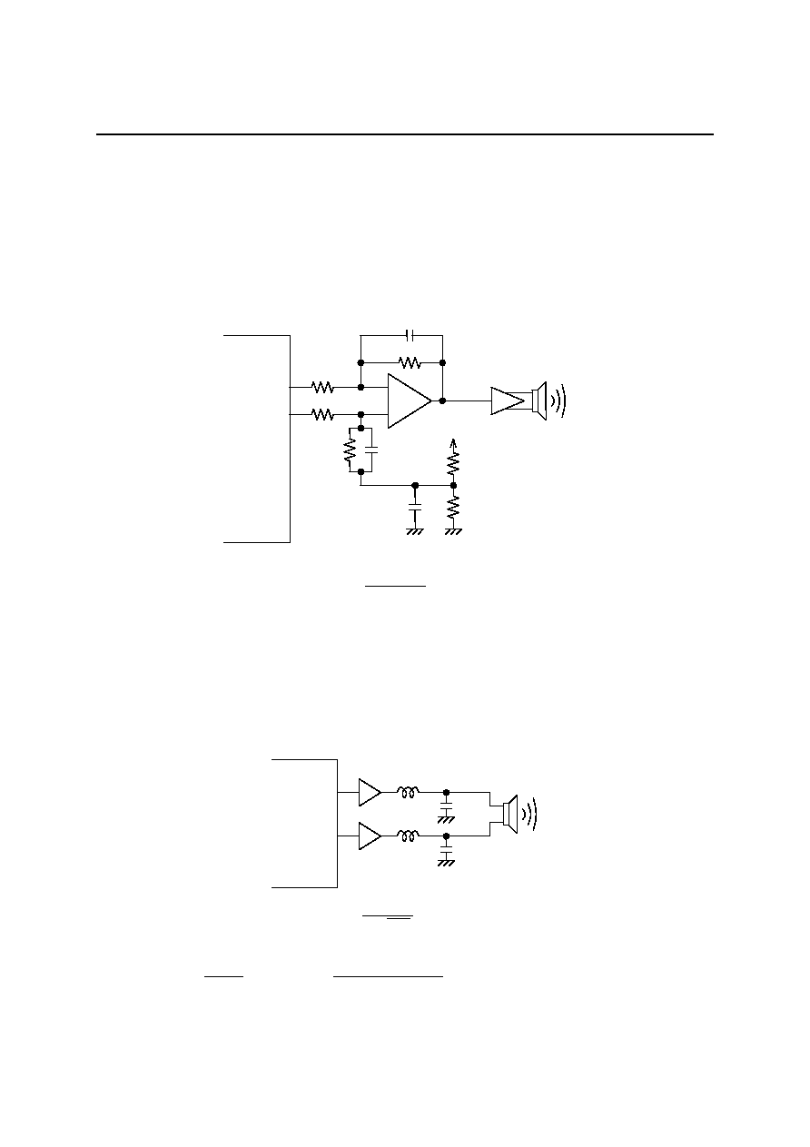
Converting PWM Signal to Analog Signal
Examples of circuits that convert the PWM output signal to an Analog signal when PWM output is selected
(OPTANA pin = "H") are given below.
1. Example Using Active LPF
The LPF primary side is configured as below using an OP amplifier.
Speaker amplifier
R
1
R
1
�
+
R
2
R
2
C
1
C
1
R
3
C
2
R
3
ML2250f
OUT(+)
OUT(�)
LPC cutoff frequency, f
C
, is determined by
Ratio of resistors R
1
to R
2
determines the voltage amplification factor. To set the amplification factor 2 times of the
OP amplifier, set R
1
:R
2
= 1:2.
2. Example Using LC Filter
Secondary LPF is configured using a coil (L) and a capacitor (C). This configuration can directly drive a speaker.
However, a buffer is required between the PWM output and the LC filter.
C
ML2250f
OUT(+)
OUT(�)
L
L
C
LPF cutoff frequency, f
C
, is determined by .
In the case of secondary Butterworth type LC filter, the constants are obtained by the following equations:
Here, R
L
stands for the output load resistance and f
C
stands for cutoff frequency of LC filter.
2
1
f
C
=
LC
2
f
C
1
L = 1.4142
�
1.412
�
R
L
�
(2
f
C
)
1
C =
2
R
2
C
1
1
f
C
=
FEDL2250DIGEST-01
OKI Semiconductor
ML2252/54-XXX, ML22Q54
28/31
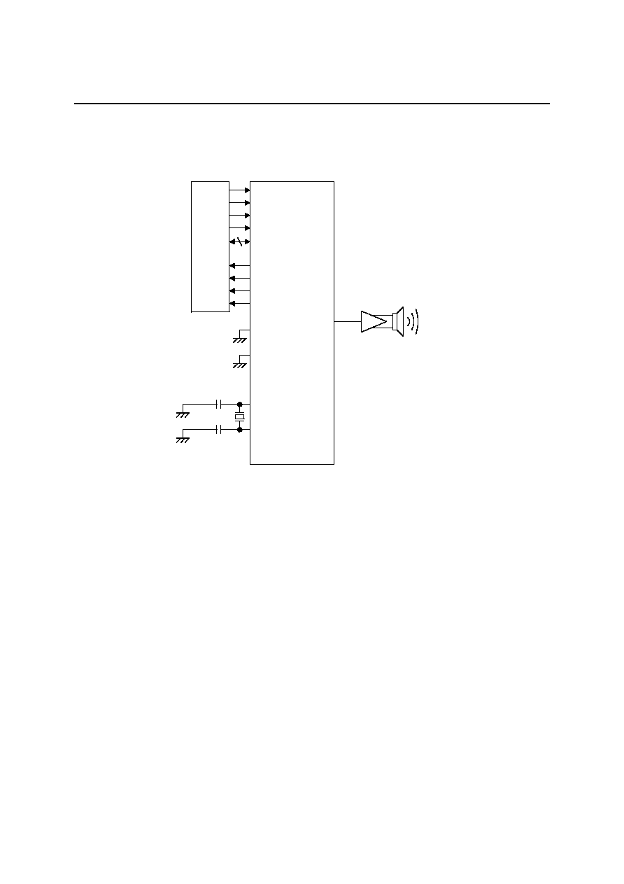
APPLICATION CIRCUIT EXAMPLE (ML2252/54-XXX, ML22Q54)
AOUT
RESET
CS
WR
RD
D7-0
NCR1
NCR2
BUSY1
BUSY2
SERIAL
OPTANA
XT
XT
MCU
8
4.096 MHz
30 pF
30 pF
Speaker amplifier
FEDL2250DIGEST-01
OKI Semiconductor
ML2252/54-XXX, ML22Q54
29/31
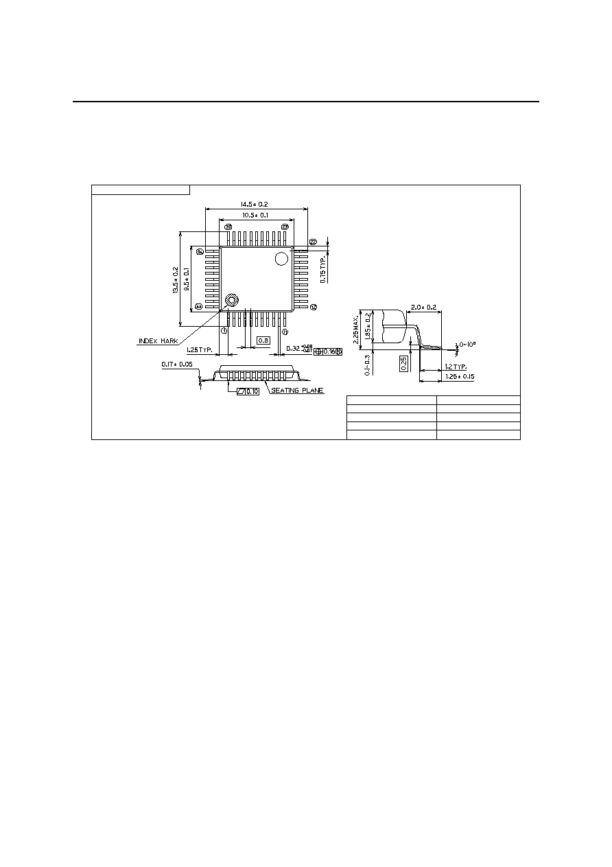
PACKAGE DIMENSIONS
QFP44-P-910-0.80-2K
Mirror finish
Package material
Epoxy resin
Lead frame material
42 alloy
Pin treatment
Solder plating (
5�m)
Package weight (g)
0.41 TYP.
5
Rev. No./Last Revised
4/Nov. 28, 1996
Notes for Mounting the Surface Mount Type Package
The surface mount type packages are very susceptible to heat in reflow mounting and humidity
absorbed in storage.
Therefore, before you perform reflow mounting, contact Oki's responsible sales person for the product
name, package name, pin number, package code and desired mounting conditions (reflow method,
temperature and times).
(Unit: mm)

FEDL2250DIGEST-01
OKI Semiconductor
ML2252/54-XXX, ML22Q54
30/31
REVISION HISTORY
Page
Document
No.
Date
Previous
Edition
Current
Edition
Description
FEDL2250DIGEST-01
Oct. 15, 2002
�
�
Final edition 1

FEDL2250DIGEST-01
OKI Semiconductor
ML2252/54-XXX, ML22Q54
31/31
NOTICE
1. The information contained herein can change without notice owing to product and/or technical improvements.
Before using the product, please make sure that the information being referred to is up-to-date.
2. The outline of action and examples for application circuits described herein have been chosen as an
explanation for the standard action and performance of the product. When planning to use the product, please
ensure that the external conditions are reflected in the actual circuit, assembly, and program designs.
3. When designing your product, please use our product below the specified maximum ratings and within the
specified operating ranges including, but not limited to, operating voltage, power dissipation, and operating
temperature.
4. Oki assumes no responsibility or liability whatsoever for any failure or unusual or unexpected operation
resulting from misuse, neglect, improper installation, repair, alteration or accident, improper handling, or
unusual physical or electrical stress including, but not limited to, exposure to parameters beyond the specified
maximum ratings or operation outside the specified operating range.
5. Neither indemnity against nor license of a third party's industrial and intellectual property right, etc. is
granted by us in connection with the use of the product and/or the information and drawings contained herein.
No responsibility is assumed by us for any infringement of a third party's right which may result from the use
thereof.
6. The products listed in this document are intended for use in general electronics equipment for commercial
applications (e.g., office automation, communication equipment, measurement equipment, consumer
electronics, etc.). These products are not authorized for use in any system or application that requires special
or enhanced quality and reliability characteristics nor in any system or application where the failure of such
system or application may result in the loss or damage of property, or death or injury to humans.
Such applications include, but are not limited to, traffic and automotive equipment, safety devices, aerospace
equipment, nuclear power control, medical equipment, and life-support systems.
7. Certain products in this document may need government approval before they can be exported to particular
countries. The purchaser assumes the responsibility of determining the legality of export of these products
and will take appropriate and necessary steps at their own expense for these.
8.
No part of the contents contained herein may be reprinted or reproduced without our prior permission.
Copyright 2002 Oki Electric Industry Co., Ltd.