1
Wednesday, February 20, 2002
ML2860 SPECIFICATION ver 1.0.0
Oki Electric Industry Co.Ltd.
ML2860 DATA SHEET
16-Tone, 32-Poly Hi-Grade PCM Sound Generator LSI
Version 1.0.1, Revised on Wednesday, February 20, 2002
GENERAL DESCRIPTION
ML2860 is a PCM-based hi-grade sound
generator LSI, develped specifically for music
ringers as used in cellular/PHS phones. With an
on-chip high-quality General MIDI sound set,
ML2860 is capable of playing 16 tones and 32
polyphonies simultaneously. Using the on-chip
three FIFOs which store musical score data,
MIDI message and ADPCM audio data, a
fantastic music ringer subsystem can readily be
built around this chip.
FEATURES
1) Supports GM System level 1
2) On-chip high-quality GM sound set
3) 128 timbres + 48 percussions embedded
4) 16 timbres, 32 polyphonies simultaneously
(default setting is 24)
5) 5V open drain ports with current control
for vibrator, front panel light, LED x 4
6) 3-wire serial / 8-bit parallel bus selectable
7) FIFO embedded for CPU power reduction
8) Power down current: 1�A (typ.)
9) Operating current: 60mA (max.)
10) Power supply: +2.7 ~ 3.3V
11) Operating temperature: -20 ~ +85�C
12) Internal stereo earphone amplifier & DAC
APPLICATION EXAMPLES
Mobile phone, PHS, Fax, PDA
(Note )
Please appreciate that ML2860 is not offered
for musical instrument and toy applications,
such as keyboards.
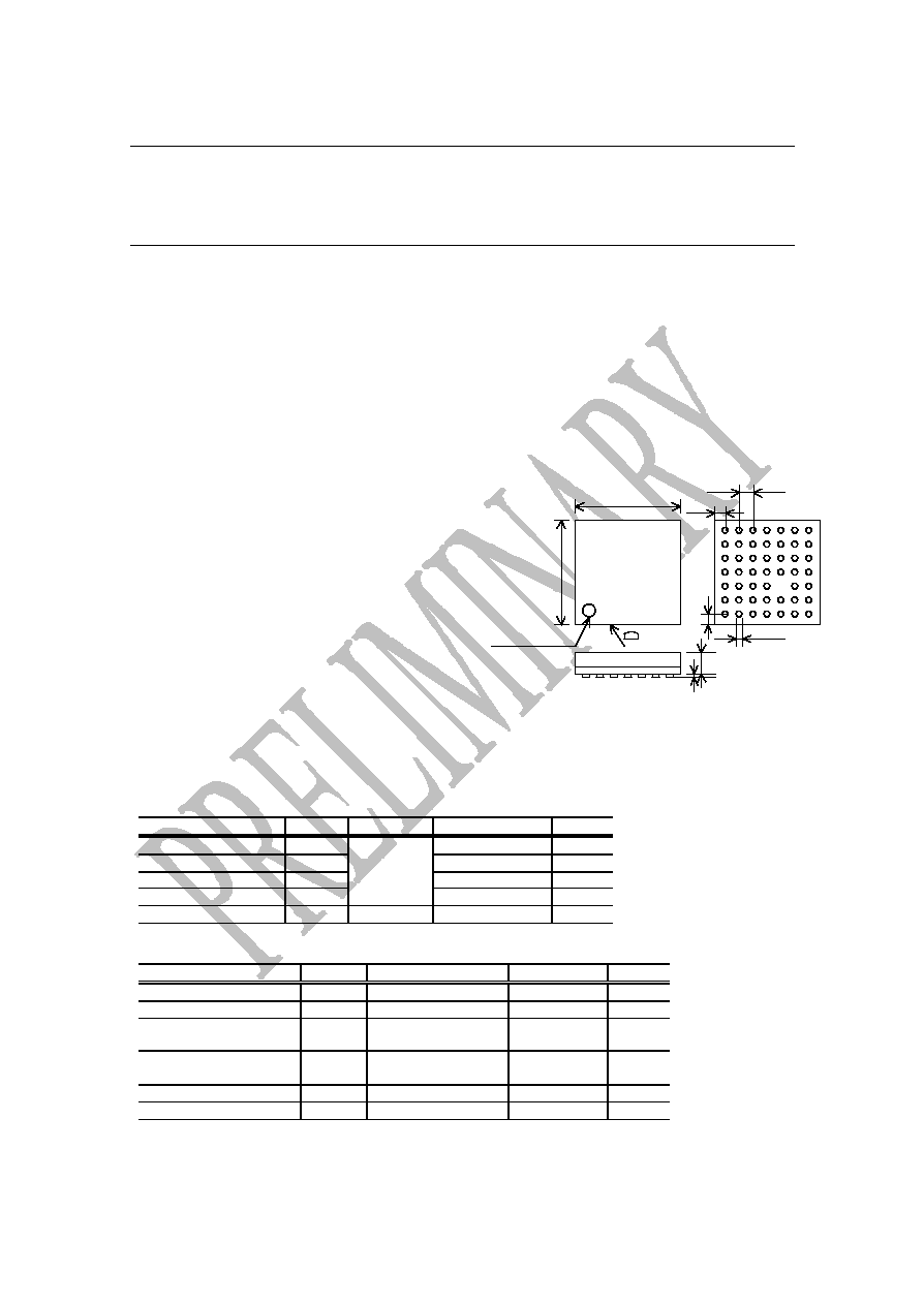
PACKAGE SPECIFICATION
48PIN W-CSP
(P-VFLGA48-6.26x5.98-0.80-W)
5.98
6.26
0.8
0.59
0.45
�
0.05
0.73
0.08
�
0.02
0.40
�
0.0
2
INDEX MARK
0.15
TOP VIEW
BOTTOM VIEW
SIDE VIEW
unit: mm(typ)
ABSOLUTE MAXIMUM RATINGS
Parameter
Symbol
Condition
Rating
Unit
Supply Voltage
VDD
Ta=25�C
-0.3 - +5.0
V
Input Voltage 1 *1
VIN
-0.3 - VDD+0.3
V
Input Voltage 2 *1
VIN
-0.3 � +5.5
V
Power Dissipation
Pd
320
mW
Storage Temperature
TSTG
-
-55 - +125
�C
RECOMMENDED OPERATING RANGES
Parameter
Symbol
Condition
Rating
Unit
Supply Voltage
DVDD
DGND=AGND=0V
2.7 - 3.3
V
Supply Voltage
AVDD
DGND=AGND=0V
DVDD
V
Supply Voltage
IOVDD
DGND=AGND=0V
Bus Interface
1.65-DVDD
V
Supply Voltage
IOVDD
DGND=AGND=0V
Serial Interface
DVDD
V
Operating Temperature
TOP
-
-20 -+85
�C
M aster clock frequency
fCLK
-
2.7- 34
MHz
1
Wednesday, February 20, 2002
ML2860 SPECIFICATION ver 1.0.0
Oki Electric Industry Co.Ltd.
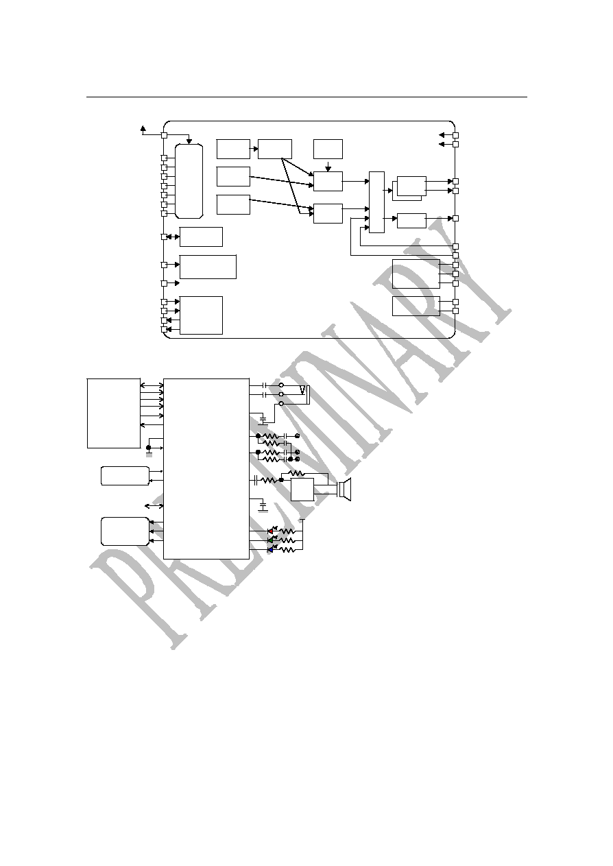
BLOCK DIAGRAM
1.8V CPU I/F
[bus I/F]
FIFO
FIFO
Sequencer
Sound
Generator
WAVE
ROM
FIFO
ADPCM
PWM
GPIO
MUX / VOL
CLOCK GEN
2.7MHz � 34MHz
BIAS
HPAMP
AOUT
TEST
TESTI
P7-0
CLK
DVDD
AVDD
XTGND
XTVDD
DRVGND
HPOUTL
HPOUTR
[Stereo]
MIXOUT
[mono]
MIXINL
MIXINR
PWM A-D
VIB
PANEL
HPSG
MIXSG
D7-0
CS
RD
WR
ILE
IRQ
IFSEL
0: BUS / 1: Serial
RESET
VDDIO[1.65-DVDD]
PTESTIN2-1
PTESTOUT2-1
TESTO
TYPICAL APPLICATION CIRCUIT
CPU
D7-0
ADR
WR
RD
Interrupt
ML2860
ADR
D7-0
CS
WR
RD
IRQ
ILE
HPOUTR
HPOUTL
PORT5-0
MIXINL
MIXOUT
External analog L
MIXINR
External analog R
External analog monaural
MIXSG
+
+
PWMA
PWMB
PWMC
5V
Red LED
Green LED
Blue LED
For system control
HPSG
SP AMP
PWMD
VIB
PANEL
IFSEL
TESTI
PTESTIN2 -1
PTESTOUT2 -1
According to system
According to system
Audio headphone
SOFTWARE SUPPORT (SUBJECT TO AN NON DISCLOSURE AGREEMENT)
a.) Support software for Standard MIDI file format 0/1 playback.
b.) Support software for MCDF (Oki original musical score format) playback.
MCDF: 1) File size compression of musical score from Standard MIDI file
2) Expand function for synchronization between picture, text, LED and MIDI.

1
Wednesday, February 20, 2002
ML2860 SPECIFICATION ver 1.0.0
Oki Electric Industry Co.Ltd.
DC CHARACTERISTICS [OUTLINE]
IOVDD=1.65-DVDD, DVDD=AVDD=+2.7V-3.3V, DGND=AGND=0V, Ta=-20-+85�C
Parameter
Symbol
Condition
Min.
Typ
Max.
Unit
"H" Input Voltage
VIH
DGND=AGND=0V
VDD x 0.8
-
-
V
"L" Input Voltage
VIL
-
-
-
VDD x 0.2
V
"H" Output Voltage
VOH
IOH=-100
�
A
VDDx0.8
-
-
V
"L" Output Voltage
VOL
IOL=100
�
A
-
-
VDDx0.2
V
"H" Input Current
IIH
VIH=VDD
-
-
10
�
A
"L" Input Current
IIL
VIL=0V
-10
-
-
�
A
Operating Current
IDDD
Sound generator
(Ports no load)
-
20
30
mA
Stereo/f=1kHz
Each drive 3mW
AC-Load = 32
-
18
-
mA
Ta=-20-+40�C
-
1
10
�
A
Ta=+40-+50�C
-
-
20
�
A
Ta=+50-+75�C
-
-
100
�
A
Standby Current
IDDS
Ta=+75-+85�C
-
-
150
�
A
AC CHARACTERISTICS / TIMING CHART [OUTLINE]
IOVDD=1.65V- DV
DD
, DV
DD
=+2.7V-3.3V, DGND=AGND=0V, Ta=-20-+85�C
BUS WRITE TIMING
Parameter
Symbol
Min
Max.
Unit
ILE valid to
Write Enable Low
tIWL
10
ns
ILE valid to
Write Enable High
tIWH
10
ns
CSB valid to
Write Enable Low
tCWL
5
ns
Write Enable
Pulse Width
tWW
25
ns
Data Valid to
Write Enable Low
tDWL
50
ns
Data Valid to
Write Enable High
tDWH
0
ns
Chip Select to
End of Write
tCEW
50
ns
BUS READ TIMING
Parameter
Symbol
Min
Max.
Unit
ILE valid to
Read Enable Low
TIRL
10
-
ns
ILE valid to
Read Enable High
TIRH
10
-
ns
Read Enable Low to
Data Valid
TRLDV
-
85
ns
Chip Enable Low to
Data Valid
TCLDV
-
85
ns
Read Enable High to
Data Transition
TRHDT
-
85
ns
Chip Enable High to
Data Transition
TCHDT
-
85
ns
tWW
D7-0
INDEX
WR
CS
tDWL tDWH
tIWH
tCEW
tIWL
INDEX
DATA
tWW
tDWL tDWH
tIWH
tCEW
tIWL
tCWL
tCWL
D7-0
INDEX
RD
CS
VALID
tCHDT
tRHDT
tCLDV
tRLDV
tIRL
tIRH
VOH
VOL
1
Wednesday, February 20, 2002
ML2860 SPECIFICATION ver 1.0.0
Oki Electric Industry Co.Ltd.
CS(I)
SCLK(I)
MODE0
SDIN(I)
1
2
8
9
11
16
tCLSH1 tCLSL1
tSL
tSH
tSC
tIDSH1 tIDSL1
tCHSH1
tCH
SDOUT (O )
tODSL
tODSL
tCHDT
10
SCLK(I)
MODE2
1
2
8
9
11
16
tCLSH2 tCLSL2
tSH
tSL
tSC
tCHSH2
tCH
10
SERIAL INTERFACE
DV
DD
=IOV
DD
=+2.7V-3.3V, DGND=AGND=0V, Ta=-20-+85�C
Parameter
Symbol
Min
Max.
Unit
Chip Select Low to SCLK Low 1
tCLSL1
50
-
ns
Chip Select Low to SCLK Low 2
tCLSL2
25
-
ns
Chip Select Low to SCLK High 1
tCLSH1
50
-
ns
Chip Select Low to SCLK High 2
tCLSH2
25
-
ns
SCLK High Pulse Width
tSH
25
-
ns
SCLK Low Pulse Width
tSL
25
-
ns
SCLK Cycle Time
tSC
50
-
ns
Input Data Valid to SCLK Low1
tIDSL1
15
-
ns
Input Data Valid to SCLK Low2
tIDSL2
15
-
ns
Input Data Valid to SCLK High1
tIDSH1
15
-
ns
Input Data Valid to SCLK High2
tIDSH2
15
-
ns
Chip Select High to SCLK Low 1
tCHSL1
0
-
ns
Chip Select High to SCLK High 2
tCHSH2
0
-
ns
Chip Select High Pulse Width
tCH
25
-
ns
Output Data Valid to SCLK Low 1
tODSL1
-
20
ns
Output Data Valid to SCLK High 2
tODSH2
-
20
ns
Chip Enable High to Data Transition
tCHDT
-
20
ns
RST High to Chip Select Low
tRSC
90
-
ns
RST Pulse Width
tRST
1
-
�
s
Initialize Time
tINIT
40
ms
DATA Write Timing
Data Read Timing
FREQUENTLY ASKED QUESTIONS
Q1. What kind of musical score formats does the ML2860 support?
A1. ML2860 can play Standard MIDI files under given conditions and the Oki original musical score format directly.
If Standard MIDI file format 1/0 or Karaoke function need to be supported, Oki provides sample software based
on NDA for this purpose.
Q2. What is the condition for playing Standard MIDI file directly?
A2.
(1) Play format 0 only, do not play format 1.
(2) Eliminate text and MIDI events not supported by the ML2860.
Q3. Which MIDI events does the ML2860 support?
A3.
-
Note On/Off / Program change / Pitch bend / Channel pressure
-
Control change [Modulation / Volume / Pan / Expression / Sustain / Reset all controller / All note off]
-
RPN [Pitch bend sensitivity / Fine tuning / Coarse tuning]
Q4. Does the ML2860 support synchronization of LED with ADPCM playback ?
A4. Yes. LED and ADPCM functions are included in the musical score and are assigned as percussion to MIDI
channel 10. It is necessary to build a software routine for this synchronization.
CS(I)
SCLK(I)
MODE0
SDIN(I)
1
2
3
15
16
tCLSL1 tCLSH1
tSL
tSH
tSC
tIDSL1 tIDSH1
tCHSL1
tCH
SCLK(I)
MODE 2
1
2
3
15
16
tCLSH2 tCLSL2
tSH
tSL
tSC
tCHSH2
tCH2