 | –≠–ª–µ–∫—Ç—Ä–æ–Ω–Ω—ã–π –∫–æ–º–ø–æ–Ω–µ–Ω—Ç: ML54053 | –°–∫–∞—á–∞—Ç—å:  PDF PDF  ZIP ZIP |

SECOND EDITION
ISSUE DATE : JAN. 1999
DATA SHEET
°
ML54053
NAND Flash Memory Controller
PRELIMINARY

NOTICE
1.
The information contained herein can change without notice owing to product and/or
technical improvements. Before using the product, please make sure that the information
being referred to is up-to-date.
2.
The outline of action and examples for application circuits described herein have been
chosen as an explanation for the standard action and performance of the product. When
planning to use the product, please ensure that the external conditions are reflected in the
actual circuit, assembly, and program designs.
3.
When designing your product, please use our product below the specified maximum
ratings and within the specified operating ranges including, but not limited to, operating
voltage, power dissipation, and operating temperature.
4.
Oki assumes no responsibility or liability whatsoever for any failure or unusual or
unexpected operation resulting from misuse, neglect, improper installation, repair, alteration
or accident, improper handling, or unusual physical or electrical stress including, but not
limited to, exposure to parameters beyond the specified maximum ratings or operation
outside the specified operating range.
5.
Neither indemnity against nor license of a third party's industrial and intellectual property
right, etc. is granted by us in connection with the use of the product and/or the information
and drawings contained herein. No responsibility is assumed by us for any infringement
of a third party's right which may result from the use thereof.
6.
The products listed in this document are intended for use in general electronics equipment
for commercial applications (e.g., office automation, communication equipment,
measurement equipment, consumer electronics, etc.). These products are not authorized
for use in any system or application that requires special or enhanced quality and reliability
characteristics nor in any system or application where the failure of such system or
application may result in the loss or damage of property, or death or injury to humans.
Such applications include, but are not limited to, traffic and automotive equipment, safety
devices, aerospace equipment, nuclear power control, medical equipment, and life-support
systems.
7.
Certain products in this document may need government approval before they can be
exported to particular countries. The purchaser assumes the responsibility of determining
the legality of export of these products and will take appropriate and necessary steps at their
own expense for these.
8.
No part of the contents cotained herein may be reprinted or reproduced without our prior
permission.
9.
MS-DOS is a registered trademark of Microsoft Corporation.
Copyright 1999 Oki Electric Industry Co., Ltd.
Printed in Japan
E2Y0002-29-11

Table of Contents
1. FEATURES ........................................................................................................... 2
2. BLOCK DIAGRAM ............................................................................................... 2
3. PIN SPECIFICATIONS ........................................................................................ 3
3.1 Host Interface ...................................................................................................... 3
3.2 NAND Flash Memory Interface .......................................................................... 4
3.3 Extended Bus Interface ...................................................................................... 5
3.4 Other Interfaces .................................................................................................. 5
3.5 Power Supply ....................................................................................................... 5
3.6 Pin Totals ............................................................................................................. 5
3.7 Pin Configuration ................................................................................................ 6
4. FUNCTIONS ........................................................................................................ 7
5. ATA REGISTERS ................................................................................................. 8
5.1 Memory Mapped Configuration ......................................................................... 8
5.2 I/O Mapped 16 Contiguous Registers Configuration ...................................... 9
5.3 Primary I/O Mapped Configuration ................................................................... 9
5.4 Secondary I/O Mapped Configuration ............................................................ 10
5.5 True IDE Mapped Configuration ...................................................................... 10
5.6 ATA Registers .................................................................................................... 11
5.6.1 Data Register (Write/Read) ...................................................................... 11
5.6.2 Error Register (Read Only) ....................................................................... 11
5.6.3 Feature Register (Write Only) ................................................................... 11
5.6.4 Sector Count Register (Write/Read) ........................................................ 11
5.6.5 Sector Number Register (Write/Read) ..................................................... 12
5.6.6 Cylinder Low Register (Write/Read) ......................................................... 12
5.6.7 Cylinder High Register (Write/Read) ........................................................ 12
5.6.8 Drive Head Register (Write/Read) ............................................................ 12
5.6.9 Status Register & Alternate Status Register (Read Only) ........................ 13
5.6.10 Device Control Register (Write Only) ....................................................... 13
5.6.11 Command Register (Write Only) .............................................................. 13
6. COMPACTFLASH INTERFACE ........................................................................ 14
6.1 ATA Commands (Standard) .............................................................................. 14
6.2 Commands for CompactFlash ......................................................................... 15
6.3 Vendor-Unique Commands .............................................................................. 15
6.4 Card Information Structure .............................................................................. 15
6.5 Identify Information ........................................................................................... 15
6.6 Number of Installed Memory Chips and CHS Structure ................................ 16
6.7 Modes ................................................................................................................. 17
6.7.1 Memory Mapped ..................................................................................... 17
6.7.2 I/O Mapped 16 Contiguous Registers ..................................................... 17
6.7.3 Primary I/O Mapped ................................................................................ 17
6.7.4 Secondary I/O Mapped ........................................................................... 17
6.7.5 True IDE ................................................................................................... 17
7. CHIP MODES .................................................................................................... 18
7.1 Types .................................................................................................................. 18
7.2 Settings .............................................................................................................. 18
7.3 Pin Assignment .................................................................................................. 18

8. ELECTRICAL CHARACTERISTICS .................................................................. 19
8.1 Absolute Maximum Ratings ............................................................................. 19
8.2 Recommended Operating Conditions ............................................................. 19
8.3 DC Characteristics ............................................................................................ 19
9. BUS SPECIFICATIONS ..................................................................................... 20
9.1 I/O Mode ........................................................................................................... 20
9.2 Bus Timing Specifications ............................................................................... 20
9.3 Power ON/OFF, Reset, Busy Timing .............................................................. 20
10. PACKAGE DIMENSIONS .................................................................................. 21
11. APPLICATION EXAMPLE ................................................................................. 22

° Semiconductor
ML54053
1/22
° Semiconductor
ML54053
NAND Flash Memory Controller
The ML54053 is a controller that integrates into a single chip a host interface that conforms to
PCMCIA, the necessary functions to control NAND memory, and a microcontroller.
Internal 256 byte RAM is provided for storage of the card information structure (CIS).
A maximum of 4 chips of 64 Mbit or larger NAND flash memory can be controlled.
E2F0019-29-13
CompactFlash
TM
is a trademark of SanDisk Corporation.
This version: Jan. 1999
Previous version: Nov. 1998
Preliminary

° Semiconductor
ML54053
2/22
1. FEATURES
∑ Single chip controller with internal microcontroller (min. 4 cycles/instruction execution)
∑ Operating voltage: 3.3 V, Interface voltage: 3.3 V/5 V
∑ Internal 256B RAM for card information structure (CIS) storage
∑ Conforms to CompactFlash specification
∑ Auto-sleep mode support
∑ True IDE Mode support
∑ ECC system by BCH code (3-bit random error correction is possible for user data and ECC data)
∑ Substitute control function (defect management function)
∑ Debug mode support
∑ High-speed operation via dual port bus control
∑ Low power consumption due to single chip controller
∑ Control of four NAND flash memories (64MB to 512MB) is possible
∑ 120-pin TQFP package
(TQFP120-P-1414-0.40-K)
2. BLOCK DIAGRAM
Host I/F
PCMCIA
ATA
NAND
Flash
Bus
CompactFlash
I/F
CIS
Media I/F
ECC
Internal RAM
MPU
RAM
ROM
External
CPU Bus

° Semiconductor
ML54053
3/22
3. PIN SPECIFICATIONS
Refer to Section 11, "Application Example" for specific connection examples.
3.1 Host Interface
Signal Name
ha [10:0]
hd [15:0]
hcen [2:1]
hiordn
hiowrn
hoen
hwen
hregn
hirqn
hstschgn
hinpackn
Type
I
B
I
I
I
I
I
I
O
O
O
Pin Count
11
16
2
1
1
1
1
1
1
1
1
Description
Address bus (A10 is MSB, A0 is LSB)
Data bus (D15 is MSB, D0 is LSB)
Card enable signal (hcen1 controls even addresses and hcen2 controls odd
addresses. The combination of ha0, hcen1 and hcen2 allows even/odd
addresses to be accessed by hd[7:0].)
I/O read signal (control signal to read data from ATA registers)
I/O write signal (control signal to write data to ATA registers)
Output enable signal
Write enable signal
Register select & I/O Enable signal
Interrupt request signal (when the card is configured as an I/O card)
Card status change signal (signal to change the status of the configuration
status register)
Input port acknowledge signal (acknowledge signal during I/O read)
hiois16n
O
1
16-bit address enable signal (when the card is configured as an I/O card,
this signal indicates that 16-bit addresses are enabled)
hwaitn
O
1
Wait signal
hspkr
B
1
Audio digital waveform signal
hrst
I
1
Reset signal
hcseln
I
1
Cable select signal (used only in True IDE Mode, GND: Master, X: Slave)
Total 42 pins
I: Input, O: Output, B: Bidirectional
° Semiconductor
ML54053
4/22
3.2 NAND Flash Memory Interface
Signal Name
maio [7:0]
macle
maale
maren
mawen
marbn
mbio [7:0]
mbcle
mbale
mbren
mbwen
Type
B
O
O
O
O
I
B
O
O
O
O
Pin Count
8
1
1
1
1
1
8
1
1
1
1
Description
Port A I/O bus
Port A command latch enable signal (signal to control latching of an
operation command into a device)
Port A address latch enable signal (signal to control latching of an address
or input data into a device)
Port A read enable signal
Port A write enable signal (signal to latch data into a device)
Port A ready/busy signal (signal to check internal status of device)
Port B I/O bus
Port B command latch enable signal (signal to control latching of an
operation command into a device)
Port B address latch enable signal (signal to control latching of an address
or input data into a device)
Port B read enable signal
Port B write enable signal (signal to latch data into a device)
mbrbn
I
1
Port B ready/busy signal (signal to check internal status of device)
mcen [3:0]
O
4
Chip enable signals
Total 31 pins
mwpn
O
1
Write protect signal (signal to forcibly prohibit write and erase operations)
3.3 Extended Bus Interface
The extended bus interface is a signal line for the ML54053's internal microcontroller. The
extended bus interface is used for purposes such as debugging.
*
In an external ROM connection mode, xah, xad, xrd, xwr, and xale are used to connect to
external ROM.
Signal Name
xah [15:8]
Type
B
Pin Count
8
Description
Address bus for extended bus
Total 23 pins
xad [7:0]
B
8
Address/data bus for extended bus
xrd
B
1
Read signal for extended bus
xwr
B
1
Write signal for extended bus
xale
B
1
Address latch enable signal for extended bus
xpsen
I
1
Program store enable signal for extended bus
xint
O
1
Interrupt signal for extended bus
xrst
O
1
Reset signal for extended bus
xclk
O
1
Clock signal for extended bus
° Semiconductor
ML54053
5/22
*
The chip mode is determined depending upon the status of pcfg[1:0] when the porn signal
rises.
pcfg[1:0] = 11 : Normal mode
pcfg[1:0] = 01 : External CPU connection mode
pcfg[1:0] = 10 : External ROM connection mode
pcfg[1:0] = 00 : Test mode (normally not used)
3.4 Other Interfaces
Signal Name
txd/pcfg [0]
Type
B
Pin Count
1
Description
Serial data I/O and chip mode setting
Total 5 pins
rxd/pcfg [1]
I
1
porn
I
1
Power-on-reset signal (connect to power monitor circuit)
xin
I
1
Clock I/O (connect a crystal oscillator between xin and xout)
xout
O
1
3.5 Power Supply
3.6 Pin Totals
Signal Name
VDD-CORE
Type
DC
Pin Count
2
Description
Power supply for core
Total 19 pins
VSS-CORE
DC
2
VDD
DC
6
Power supply for I/O pad
VSS
DC
9
NAND Flash Memory Interface
31
Host Interface
42
Extended Bus Interface
23
Other Interfaces
5
Power Supply
19
Total
120
° Semiconductor
ML54053
6/22
3.7 Pin Configuration
89
88
87
86
85
84
83
82
81
80
79
78
77
76
75
74
73
72
71
70
69
68
67
66
65
64
63
62
61
hd3
hd11
hd4
hd12
VDD
hd5
hd13
hd6
hd14
VSS
hd7
hd15
hce1n
hce2n
ha10
VSS-CORE
hoen
hiordn
ha9
hiowrn
ha8
hwen
ha7
hirqn
ha6
hcseln
ha5
ha4
hrst
ha3
1
1
2
3
4
5
6
7
8
9
10
11
12
13
14
15
16
17
18
19
20
21
22
23
24
25
26
27
28
29
30
mwpn
macle
maale
xout
VSS
xin
maren
mawen
marbn
VDD
maio0
maio7
maio1
maio6
VSS
VSS-CORE
maio2
maio5
maio3
maio4
VDD
mcen0
mcen1
mcen2
mcen3
VSS
mbcle
mbale
mbren
mbwen
120
119
118
117
116
115
114
113
112
111
110
109
108
107
106
105
104
103
102
101
100
99
98
97
96
95
94
93
92
91
porn
rxd
txd
xpsen
xint
xrst
xclk
xale
xrdn
xwrn
xad7
VSS
xad6
xad5
VDD-CORE
xad4
VDD
xad3
xad2
xad1
xad0
xa15
xa14
xa13
xa12
xa11
VSS
xa10
xa9
xa8
31
32
33
34
35
36
37
38
39
40
41
42
43
44
45
46
47
48
49
50
51
52
53
54
55
56
57
58
59
60
mbrbn
mbio0
mbio7
mbio1
mbio6
VSS
mbio2
mbio5
mbio3
VDD
mbio4
VSS
hd10
hiois16n
VDD-CORE
hd9
hd2
hd8
hd1
hstschgn
VDD
hd0
hspkr
VSS
ha0
hregn
ha1
hinpackn
ha2
hwaitn
ML54053
90
120-Pin Plastic TQFP

° Semiconductor
ML54053
7/22
4. FUNCTIONS
(1)
Sector Formatter and Sequencer
The sector formatter and sequencer control the logical format of the NAND flash memory
and efficiently perform defect management (substitute processing).
(2)
CompactFlash Interface
The PCMCIA interface conforms to CompactFlash specification.
(3)
Chip Modes
An external ROM connection mode for the ML54053's internal microcontroller and an
external CPU connection mode are supported. With these modes, evaluation can be
performed efficiently.
(4)
Auto-Sleep Mode
If there is no access from the host over a specific period of time, operation automatically
transfers to the sleep mode.
(5)
Dual Port Bus Control Mode
When erasing data or writing the same data, two port buses (Port A, Port B) can be utilized
simultaneously for high-speed operation.

° Semiconductor
ML54053
8/22
5. ATA REGISTERS
When a mode such as memory mode or I/O mode is configured, the host must use different
addresses for access.
5.1 Memory Mapped Configuration
* Don't care
-CE1 -CE2 -REG A10 A9-A4 A3-A0
Read (-OE = L)
Write (-WE = L)
*
*
*
*
*
*
*
*
*
*
*
*
*
*
*
*
*
*
*
*
*
*
*
*
0
0
0
1
0
0
1
0
0
1
0
0
1
0
0
0
1
0
1
0
0
1
0
0
0
1
0
1
1
0
1
1
0
1
1
0
1
1
0
0
1
1
0
1
0
1
1
0
0
1
1
0
1
1
1
1
1
1
1
1
1
1
1
1
1
1
1
1
1
1
1
1
1
1
1
1
1
1
0
0
0
0
0
0
0
0
0
0
0
0
0
0
0
0
0
0
0
0
0
0
1
1
1
1
*
(000x)
0h
1h
(000x)
2h
3h
(001x)
4h
5h
(010x)
6h
7h
(011x)
(100x)
8h
9h
(100x)
Dh
(110x)
Eh
Fh
(111x)
*
(xxx0)
(xxx1)
*
16-bit Data
8-bit Data
Error
Error
Sector Count
Sector Number
Sector Number
Cylinder Low
Cylinder High
Cylinder High
Drive/Head
Status
Status
Duplicate Data
Duplicate Even
Duplicate Odd
Duplicate Odd
Duplicate Error
Duplicate Error
Alternate Status
Drive Address
Drive Address
16-bit Data
Even Data
Odd Data
Odd Data
16-bit Data
8-bit Data
Features
Features
Sector Count
Sector Number
Sector Number
Cylinder Low
Cylinder High
Cylinder High
Drive/Head
Command
Command
Duplicate Data
Duplicate Even
Duplicate Odd
Duplicate Odd
Duplicate Features
Duplicate Features
Device Control
Not Used
Not Used
16-bit Data
Even Data
Odd Data
Odd Data
D15 : D0
D7 : D0
D7 : D0
D15 : D8
D7 : D0
D7 : D0
D15 : D8
D7 : D0
D7 : D0
D15 : D8
D7 : D0
D7 : D0
D15 : D8
D15 : D0
D7 : D0
D7 : D0
D15 : D8
D7 : D0
D15 : D8
D7 : D0
D7 : D0
D15 : D8
D15 : D0
D7 : D0
D7 : D0
D15 : D8
D15 : D0
D7 : D0
D7 : D0
D15 : D8
D7 : D0
D7 : D0
D15 : D8
D7 : D0
D7 : D0
D15 : D8
D7 : D0
D7 : D0
D15 : D8
D15 : D0
D7 : D0
D7 : D0
D15 : D8
D7 : D0
D15 : D8
D7 : D0
D15 : D0
D7 : D0
D7 : D0
D15 : D8
*

° Semiconductor
ML54053
9/22
5.2 I/O Mapped 16 Contiguous Registers Configuration
-CE1 -CE2 -REG
A9-A0
Read (-IORD = L)
Write (-IOWR = L)
1F0h
1F0h
1F1h
1F0h/1F1h
1F2h
1F3h
1F2h/1F3h
1F4h
1F5h
1F4h/1F5h
1F6h
1F7h
1F6h/1F7h
3F6h
3F7h
3F6h/3F7h
0
0
0
1
0
0
1
0
0
1
0
0
1
0
0
1
0
1
1
0
1
1
0
1
1
0
1
1
0
1
1
0
0
0
0
0
0
0
0
0
0
0
0
0
0
0
0
0
16-bit Data
8-bit Data
Error
Error
Sector Count
Sector Number
Sector Number
Cylinder Low
Cylinder High
Cylinder High
Drive/Head
Status
Status
Alternate Status
Drive Address
Drive Address
16-bit Data
8-bit Data
Features
Features
Sector Count
Sector Number
Sector Number
Cylinder Low
Cylinder High
Cylinder High
Drive/Head
Command
Command
Device Control
Not Used
Not Used
D15 : D0
D7 : D0
D7 : D0
D15 : D8
D7 : D0
D7 : D0
D15 : D8
D7 : D0
D7 : D0
D15 : D8
D7 : D0
D7 : D0
D15 : D8
D7 : D0
D7 : D0
D15 : D8
D15 : D0
D7 : D0
D7 : D0
D15 : D8
D7 : D0
D7 : D0
D15 : D8
D7 : D0
D7 : D0
D15 : D8
D7 : D0
D7 : D0
D15 : D8
D7 : D0
* Don't care
-CE1 -CE2 -REG A9-A4 A3-A0
Read (-IORD = L)
Write (-IOWR = L)
*
*
*
*
*
*
*
*
*
*
*
*
*
*
*
*
*
*
*
*
*
*
0
0
0
1
0
0
1
0
0
1
0
0
1
0
0
0
1
0
1
0
0
1
0
1
1
0
1
1
0
1
1
0
1
1
0
0
1
1
0
1
0
1
1
0
0
0
0
0
0
0
0
0
0
0
0
0
0
0
0
0
0
0
0
0
0
0
0h
0h
1h
(000x)
2h
3h
(001x)
4h
5h
(010x)
6h
7h
(011x)
8h
8h
9h
(100x)
Dh
(110x)
Eh
Fh
(111x)
16-bit Data
8-bit Data
Error
Error
Sector Count
Sector Number
Sector Number
Cylinder Low
Cylinder High
Cylinder High
Drive/Head
Status
Status
Duplicate Data
Duplicate Even
Duplicate Odd
Duplicate Odd
Duplicate Error
Duplicate Error
Alternate Status
Drive Address
Drive Address
16-bit Data
8-bit Data
Features
Features
Sector Count
Sector Number
Sector Number
Cylinder Low
Cylinder High
Cylinder High
Drive/Head
Command
Command
Duplicate Data
Duplicate Even
Duplicate Odd
Duplicate Odd
Duplicate Features
Duplicate Features
Device Control
Not Used
Not Used
D15 : D0
D7 : D0
D7 : D0
D15 : D8
D7 : D0
D7 : D0
D15 : D8
D7 : D0
D7 : D0
D15 : D8
D7 : D0
D7 : D0
D15 : D8
D15 : D0
D7 : D0
D7 : D0
D15 : D8
D7 : D0
D15 : D8
D7 : D0
D7 : D0
D15 : D8
D15 : D0
D7 : D0
D7 : D0
D15 : D8
D7 : D0
D7 : D0
D15 : D8
D7 : D0
D7 : D0
D15 : D8
D7 : D0
D7 : D0
D15 : D8
D15 : D0
D7 : D0
D7 : D0
D15 : D8
D7 : D0
D15 : D8
D7 : D0
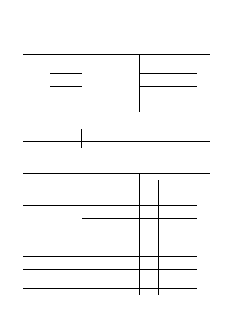
5.3 Primary I/O Mapped Configuration

° Semiconductor
ML54053
10/22
5.4 Secondary I/O Mapped Configuration
-CE1 -CE2 -REG
A9-A0
Read (-IORD = L)
Write (-IOWR = L)
170h
170h
171h
170h/171h
172h
173h
172h/173h
174h
175h
174h/175h
176h
177h
176h/177h
376h
377h
376h/377h
0
0
0
1
0
0
1
0
0
1
0
0
1
0
0
1
0
1
1
0
1
1
0
1
1
0
1
1
0
1
1
0
0
0
0
0
0
0
0
0
0
0
0
0
0
0
0
0
16-bit Data
8-bit Data
Error
Error
Sector Count
Sector Number
Sector Number
Cylinder Low
Cylinder High
Cylinder High
Drive/Head
Status
Status
Alternate Status
Drive Address
Drive Address
16-bit Data
8-bit Data
Features
Features
Sector Count
Sector Number
Sector Number
Cylinder Low
Cylinder High
Cylinder High
Drive/Head
Command
Command
Device Control
Not Used
Not Used
D15 : D0
D7 : D0
D7 : D0
D15 : D8
D7 : D0
D7 : D0
D15 : D8
D7 : D0
D7 : D0
D15 : D8
D7 : D0
D7 : D0
D15 : D8
D7 : D0
D7 : D0
D15 : D8
D15 : D0
D7 : D0
D7 : D0
D15 : D8
D7 : D0
D7 : D0
D15 : D8
D7 : D0
D7 : D0
D15 : D8
D7 : D0
D7 : D0
D15 : D8
D7 : D0
5.5 True IDE Mapped Configuration
∑ Command Block Register
* Don't care
-CE1 -CE2 -REG A9-A3 A2-A0
Read (-IORD = L)
Write (-IOWR = L)
*
*
*
*
*
*
*
*
*
0
0
0
0
0
0
0
0
0
1
1
1
1
1
1
1
1
0
0
0
0
0
0
0
0
0
0
0h
1h
2h
3h
4h
5h
6h
7h
(xxx)
16-bit Data
Error
Sector Count
Sector Number
Cylinder Low
Cylinder High
Drive/Head
Status
Not Used
16-bit Data
Features
Sector Count
Sector Number
Cylinder Low
Cylinder High
Drive/Head
Command
Not Used
D15 : D0
D7 : D0
D7 : D0
D7 : D0
D7 : D0
D7 : D0
D7 : D0
D7 : D0
D15 : D0
D7 : D0
D7 : D0
D7 : D0
D7 : D0
D7 : D0
D7 : D0
D7 : D0
* Don't care
-CE1 -CE2 -REG A9-A3 A2-A0
Read (-IORD = L)
Write (-IOWR = L)
*
*
*
*
*
1
1
1
1
1
1
0
0
0
0
0
0
0
0
0
(xxx)
(0xx)
(10x)
6h
7h
High Impedance
High Impedance
High Impedance
Alternate Status
Drive Address
Not Used
Not Used
Not Used
Device Control
Not Used
D17 : D0
D7 : D0
D7 : D0
∑ Control Block Register

° Semiconductor
ML54053
11/22
5.6 ATA Registers
ATA registers realize functions of the PC Card ATA Specifications.
5.6.1
Data Register (Write/Read)
This 16-bit or 8-bit register is used in the transfer of data blocks between the internal data buffer
and the host. Data can be transferred via consecutive 16-bit or 8-bit accesses to the data register.
5.6.2
Error Register (Read Only)
Additional information regarding the cause of a processing error in the previously executed
command is indicated. If the error bit of the status register has been set, the host must examine
this register.
D7
BBK
D6
UNC
D5
0
D4
IDNF
D3
0
D2
ABRT
D1
0
D0
AMNF
BBK
: This bit is set when a Bad Block is detected.
UNC : This bit is set when an Uncorrectable Error is encountered.
IDNF : The requested sector ID is in error or cannot be found.
ABRT : This bit is set if the command has been aborted or when an invalid command has been
issued.
AMNF : This bit is set in case of a general error.
5.6.3
Feature Register (Write Only)
This register is used to write information related to commands.
D7
D6
D5
D4
Feature Bytes
D3
D2
D1
D0
5.6.4
Sector Count Register (Write/Read)
This register is used to specify the number of sectors or address of logical blocks to be processed
by a command. By reading this register after a command has been completed, the host can check
the number of sectors not processed by the command.
D7
D6
D5
D4
Sector Count
D3
D2
D1
D0

° Semiconductor
ML54053
12/22
5.6.5
Sector Number Register (Write/Read)
This register is used to specify the sector number or logical block address where processing by
the command will begin. By reading this register after a command has been completed, the host
can check the sector number or logical block address processed by the command.
D7
D6
D5
D4
Sector Number/LBA7-LBA0
D3
D2
D1
D0
5.6.6
Cylinder Low Register (Write/Read)
This register is used to specify the lower cylinder number or the logical block address where
processing by the command will begin. By reading this register after a command has been
completed, the host can check the last lower cylinder number or logical block address that was
processed by the command.
D7
D6
D5
D4
Cylinder Low/LBA15-LBA8
D3
D2
D1
D0
5.6.7
Cylinder High Register (Write/Read)
This register is used to specify the upper cylinder number or the logical block address where
processing by the command will begin. By reading this register after a command has been
completed, the host can check the last upper cylinder number or logical block address that was
processed by the command.
D7
D6
D5
D4
Cylinder High/LBA23-LBA16
D3
D2
D1
D0
5.6.8
Drive Head Register (Write/Read)
This register is used to specify the head number or the logical block address where processing
by the command will begin. By reading this register after a command has been completed, the
host can check the last upper head number or logical block address that was processed by the
command.
D7
1
D6
LBA
D5
1
D4
DRV#
D3
HS3/LBA27
D2
HS2/LBA26
D1
HS1/LBA25
D0
HSO/LBA24
LBA:
1: LBA (logical block address) mode
0: CHS address mode
DRV#:
card number
0: drive 0 is selected
1: drive 1 is selected
If the value of the Drive# bit of the socket copy register matches the value of this bit, this
controller will execute the command.

° Semiconductor
ML54053
13/22
5.6.9
Status Register & Alternate Status Register (Read Only)
This register indicates the internal status of the controller. When the host reads this register, the
controller clears pending interrupt requests. However, even if the alternate status register is
read, interrupts requests will not be cleared.
D7
BUSY
D6
RDY
D5
DWF
D4
DSC
D3
DRQ
D2
CORR
D1
IDX
D0
ERR
BUSY:
This bit is set in the following cases:
∑ from the time when the host writes a command to the command register
until processing of the command is completed
∑ when hardware and software resets have been executed from the host
RDY:
This bit indicates Drive Ready.
DWF:
This bit is set when an error related to substitute processing occurs during
access to the internal flash memory. If this bit is set, commands that follow
may not execute properly.
DSC:
This bit is always set to 1.
DRQ:
During execution of a command that involves data transfer, this bit is set once
the transfer preparations are made.
CORR:
This bit indicates that a correctable error has occurred during access to flash
memory.
IDX:
This bit is always set to 0.
ERR:
This bit is set when an error occurs during command execution. Detailed
information is set in the error register.
5.6.10 Device Control Register (Write Only)
This register is used to control interrupt requests from the card and to specify software reset.
D7
D6
D5
X
D4
D3
1
D2
SRST
D1
-IEN
D0
0
SRST:
While this bit is 1, the controller is in the reset state.
-IEN:
1: Interrupt signal mask, 0: Interrupt signal non-mask
5.6.11
Command Register (Write Only)
This register is used to set the command code.
D7
D6
D5
D4
Command Code
D3
D2
D1
D0

° Semiconductor
ML54053
14/22
6. COMPACTFLASH INTERFACE
6.1 ATA Commands (Standard)
Supported ATA commands are listed below.
Code
Command
FR
SC
SN
CY
DH
C/R/W
--
--
--
--
--
--
--
--
--
--
--
--
--
--
--
--
--
--
--
--
Check Power Mode
Execute Drive Diagnostic
Format Track
Identify Drive
Idle
Idle Immediate
Initialize Drive Parameters
Read Buffer
Read Long Sector
Read Multiple
Read Sector (s)
Read Verify Sector (s)
Recalibrate
Seek
Set Features
Set Multiple Mode
Set Sleep Mode
Standby
Standby Immediate
Write Buffer
Write Long Sector
Write Multiple
Write Sector (s)
98h, E5h
90h
50h
ECh
97h, E3h
95h, E1h
91h
E4h
22h, 23h
C4h
20h, 21h
40h, 41h
1xh
7xh
EFh
C6h
99h, E6h
96h, E2h
94h, E0h
E8h
32h, 33h
C5h
30h, 31h
C
C
W
R
C
C
C
R
R
R
R
C
C
C
C
C
C
C
C
W
W
W
W
--
--
--
--
--
--
--
--
--
--
--
--
--
--
--
--
--
--
--
--
--
--
--
--
--
--
--
--
--
--
--
--
--
--
--
--
--
--
--
--
--
--
--
--
--
FR: Features register
SC: Sector count register
SN: Sector number register
CY: Cylinder register
DH: Drive/head register
C/R/W: C - Control, R - Read, W - Write
: modified, valid
-- : invalid

° Semiconductor
ML54053
15/22
6.2 Commands for CompactFlash
Supported CompactFlash commands are listed below.
Code
Command
FR
SC
SN
CY
DH
C/R/W
--
--
--
--
--
--
Request Sense
Erase Sector (s)
Translate Sector
Wear Level
Write Multiple w/o Erase
Write Sector (s) w/o Erase
03h
C0h
87h
F5h
CDh
38h
C
C
R
C
W
W
--
--
--
--
--
--
6.3 Vendor-Unique Commands
Vendor-unique commands can be executed by writing "FFh" data to the command register when
a value from the below chart has been written to the feature register.
Command
Code
FR
C/R/W
Low Level Format
Change Information
Change Physical Cylinder
Read All
Un Lock
C
W
C
R
C
Description
Initialization of substitute information, all sectors
Change CIS/Identify information
Set maximum value of physical cylinder
Read 528 bytes of the specified page
Vendor-unique commands that follow are valid
FFh
Undefined
FFh
Undefined
FFh
Undefined
FFh
Undefined
FFh
Undefined
Change Physical Cylinder: Sets the maximum value of the user area that is accessible from the
host. For details, refer to section 6.6, "Number of Installed Memory Chips and CHS Structure."
6.4 Card Information Structure
The desired card information structure (CIS) can be stored by the change information command.
6.5 Identify Information
The desired identify information can be stored by the change information command.

° Semiconductor
ML54053
16/22
6.6 Number of Installed Memory Chips and CHS Structure
NAND flash memory is erased in block units. Since block erasing is also performed during a 1-
page (sector) write, efficiency is increased during write operations by serially addressing sectors
within the same block.
The CHS structure and number of installed memory chips when using 64, 128, 256 and 512 Mbit
memory are listed below (where C is the default value). The C value of the CHS address can be
set by the change physical cylinder command (a vendor-unique command).
∑ 64 Mbit Memory
Capacity
No. of Chips
CHS
H
LBA Max. (Hex)
C
S
8
16
32
1
2
4
1000
1000
1000
1
1
2
16
32
32
16000
32000
64000
(3E80)
(7D00)
(FA00)
∑ 128 Mbit Memory
Capacity
No. of Chips
CHS
H
LBA Max. (Hex)
C
S
16
32
64
1
2
4
1000
1000
1000
1
1
2
32
64
64
32000
64000
128000
(7D00)
(FA00)
(1F400)
∑ 256 Mbit Memory
Capacity
No. of Chips
CHS
H
LBA Max. (Hex)
C
S
32
64
128
1
2
4
1000
1000
1000
2
2
4
32
64
64
64000
128000
256000
(FA00)
(1F400)
(3E800)
∑ 512 Mbit Memory
Capacity
No. of Chips
CHS
H
LBA Max. (Hex)
C
S
64
128
256
1
2
4
1000
1000
1000
4
4
8
32
64
64
128000
256000
512000
(1F400)
(3E800)
(7D000)

° Semiconductor
ML54053
17/22
6.7 Modes
6.7.1
Memory Mapped
In the memory mapped mode, ATA registers appear in the 0 to 2K window of common memory
space.
6.7.2
I/O Mapped 16 Contiguous Registers
In the I/O mapped 16 contiguous registers mode, contiguous ATA registers appear in I/O space.
6.7.3
Primary I/O Mapped
In the primary I/O mapped mode, ATA registers appear in 1F0h to 1F7h and 3F6h to 3F7h of the
standard I/O address space.
6.7.4
Secondary I/O Mapped
In the secondary I/O mapped mode, ATA registers appear in 170h to 177h and 376h to 377h of
the standard I/O address space.
6.7.5
True IDE
This mode is compatible with True IDE Mode.
° Semiconductor
ML54053
18/22
7. CHIP MODES
7.1 Types
There are four types of chip modes. Note that default pin assignments change depending upon
the chip mode.
∑ Normal Mode
This mode is normally used.
∑ External ROM Connection Mode
This mode is used for connection to external ROM.
∑ External CPU Connection Mode
This mode is used for debugging. When this mode is activated, the internal microcontroller
does not operate.
∑ Test Mode
This mode is used for testing. The test mode is not normally used.
7.2 Settings
Chip modes are determined by the status of pcfg[1:0] when the power-on-reset signal (porn
signal) rises.
pcfg [1 : 0] = 11
Normal Mode
pcfg [1 : 0] = 01
External CPU Connection Mode
pcfg [1 : 0] = 10
External ROM Connection Mode
pcfg [1 : 0] = 00
Test Mode
7.3 Pin Assignment
Interface
Normal
External ROM Connection
External CPU Connection
Signal Name
Extended Bus
(Low-Level)
xah [15 : 8]
xah [15 : 8]
xah [15 : 8]
O
I/O
I/O
Extended Bus
(Low-Level)
xad [7 : 0]
xad [7 : 0]
xad [7 : 0]
O
I/O
I/O
Extended Bus
(Low-Level)
xrd
xrd
xrd
O
O
I
Extended Bus
(Low-Level)
xwr
xwr
xwr
O
O
I
Extended Bus
(Low-Level)
xale
xale
xale
O
O
I
Extended Bus
(Low-Level)
(Low-Level)
xint
xint
O
O
O
Extended Bus
(Low-Level)
(Low-Level)
xpsenn
xpsenn
I
I
I
Extended Bus
(Low-Level)
(Low-Level)
xrst
xrst
O
O
O
Extended Bus
(Low-Level)
(Low-Level)
xclk
xclk
O
O
O
° Semiconductor
ML54053
19/22
8. ELECTRICAL CHARACTERISTICS
8.1 Absolute Maximum Ratings
Parameter
Power Supply Voltage
Input Voltage
Output Voltage
Input Current
Symbol
V
DD
V
I
V
O
I
I
Condition
Tj = 25∞C
Rating
≠0.3 to +4.6
≠0.3 to V
DD
+ 0.3
≠0.3 to V
DD
+ 0.3
≠10 to +10
Unit
mA
The standard is
≠0.3 to +6.0
≠0.3 to +6.0
≠6 to +6
V
Storage Temperature
Tstg
≠65 to +150
∞C
Normal Buffer
Normal Buffer
Normal Buffer
5 V Tolerant Buffer
5 V Tolerant Buffer
5 V Tolerant Buffer
V
SS
= 0 V
8.2 Recommended Operating Conditions
Parameter
Power Supply Voltage
Symbol
V
DD
Range
3.0 to 3.6
Unit
V
Operating Temperature
Tj
≠40 to +85
∞C
8.3 DC Characteristics
Parameter
Symbol
V
IH
Condition
TTL normal input
5 V tolerant input
Rating
--
Unit
2.0
V
DD
+ 0.3
High Level Input Voltage
V
Low Level Input Voltage
V
IL
--
--
≠0.3
+0.8
Schmitt Trigger Threshold Voltage
V
t+
--
1.5
--
2.0
High Level Output Voltage
V
OH
I
OH
= ≠100 mA
--
V
DD
≠ 0.2
--
Low Level Output Voltage
V
OL
I
OH
= ≠100 mA
--
--
0.2
High Level Input Current
I
IH
V
IH
= V
DD
0.01
--
1
Low Level Input Current
I
IL
V
IL
= V
SS
+0.01
mA
≠1
--
(V
DD
= 3.0 to 3.6 V, V
SS
= 0 V, Tj = ≠40 to +85∞C)
Typ.
Min.
Max.
Output Leakage Current
I
OZH
V
OL
= V
DD
0.01
--
1
Standby Power Supply Current
I
DDS
Output open
--
≠10
+10
--
2.0
5.5
--
1.0
0.7
--
V
t+
≠ V
t≠
0.5
0.4
--
I
OL
= 2, 4, 8 mA
--
2.4
--
I
OL
= 2, 4, 8 mA
--
--
0.4
(50 kW pull-up)
≠66
≠170
≠15
V
OL
= V
SS
≠0.01
≠1
--
(50 kW pull-up)
≠66
≠170
≠15
V
t≠
I
OZL
DV
t
Note 1 : Listed values are for a normal buffer and a 5 V tolerant buffer unless otherwise
specified.
Note 2 : Typical values are indicated for a typical condition at V
DD
= 3.3 V and Tj = 25
∞
C.

° Semiconductor
ML54053
20/22
9. BUS SPECIFICATIONS
9.1 I/O Mode
The I/O mode conforms to CompactFlash and IDE specifications.
9.2 Bus Timing Specifications
Bus timing conforms to CompactFlash, IDE and NAND flash memory specifications.
9.3 Power ON/OFF, Reset, Busy Timing
Parameter
Symbol
V
I
(CE)
Condition
0 V £ V
CC
< 2.0 V
2.0 V £ V
CC
< V
IH
Specified Value
Unit
0
V
I
Max.
-CE Signal Level
ms
Reset Setup Time
tsu (RESET)
--
TBD
Reset Width
tw (RESET)
--
TBD
Min.
Max.
V
CC
≠ 0.1
V
I
Max.
--
TBD
--
TBD
th (Hi-Z RESET)
ts (Hi-Z RESET)
V
IH
£ V
CC
V
IH
V
I
Max.
Ready Release Delay Time
td (BSY)
--
TBD
-CE Recovery Time
trec (V
CC
)
--
TBD
V
CC
Rise Time
tpr
10%∆(V
CC
+ 5%) 90% *1
TBD
V
CC
Fall Time
tpf
(V
CC
≠ 5%) 90%∆10% *1
TBD
ms
ms
ms
ms
ms
ms
ms
V
*1:
tpr and tpf are defined as the time of the "straight-line change from 10% to 90% of V
CC
",
and vice-versa. Even if the rise and fall waveforms are non-linear, the maximum slope of
the waveform must meet these specifications.
+RDY/-BSY
RESET
RESET
tw(RESET)
td(BSY)
th(Hi-Z RESET)
ts(Hi-Z RESET)
V
IH
V
IH
tsu(CE)
Hi-Z
Hi-Z
V
CC
-CE1, -CE2
-CE1, -CE2
V
CC
tsu(RESET)
tpr
2 V
2 V
,
trec(V
CC
)
tpf

° Semiconductor
ML54053
21/22
10. PACKAGE DIMENSIONS
(Unit : mm)
Notes for Mounting the Surface Mount Type Package
The SOP, QFP, TSOP, TQFP, LQFP, SOJ, QFJ (PLCC), SHP, and BGA are surface mount type
packages, which are very susceptible to heat in reflow mounting and humidity absorbed in
storage. Therefore, before you perform reflow mounting, contact Oki's responsible sales person
on the product name, package name, pin number, package code and desired mounting conditions
(reflow method, temperature, and times).
Package material
Lead frame material
Pin treatment
Solder plate thickness
Package weight (g)
Epoxy resin
42 alloy
Solder plating
5 mm or more
TYP.
TQFP120-P-1414-0.40-K
Mirror finish
° Semiconductor
ML54053
22/22
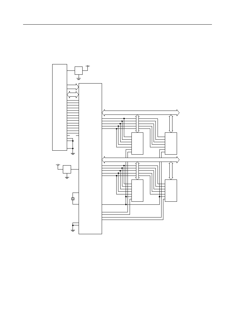
11. APPLICATION EXAMPLE
hcen1
hcen2
hoen
hwen
hirqn
hiois16n
hiordn
hiowrn
hrst
hwaitn
hinpackn
hregn
hspkr
hstschgn
maren
mawen
marbn
macle
maale
hcseln
porn
rxd
txd
mcen1
-CE1
VCC
-CE2
-OE
-WE
RDY/-BSY/-IREQ
WP/-IOIS16
-IORD
-IOWR
RST
-WAIT
-INPACK
-REG
SPKR
-STSCHG
-CD1
-CD2
GND
A25
hd0-15
D0-15
Data
ha0-10
A0-10
Connecter
Address
ML54053
ALE
-WP
-CE
R/-B
1
CLE
-RE
-WE
I/O1-8
maio0-7
5 to 3
Cnv
xout
xin
20 MHz
mcen0
mwpn
mcen3
mcen2
Vlt
Dct
Address/Data
ALE
-WP
-CE
R/-B
3
CLE
-RE
-WE
I/O1-8
mbren
mbwen
mbrbn
mbcle
mbale
ALE
-WP
-CE
R/-B
2
CLE
-RE
-WE
I/O1-8
mbio0-7
ALE
-WP
-CE
R/-B
4
CLE
-RE
-WE
I/O1-8
Address/Data