 | –≠–ª–µ–∫—Ç—Ä–æ–Ω–Ω—ã–π –∫–æ–º–ø–æ–Ω–µ–Ω—Ç: ML6190B | –°–∫–∞—á–∞—Ç—å:  PDF PDF  ZIP ZIP |

OKI Semiconductor
FEDL6190B-01
Issue Date: Mar. 3, 2005
ML6190B
Longwave Time Code RF Receiver LSI
1/11
GENERAL DESCRIPTION
The ML6190B receives and detects standard low-frequency radio waves and outputs time codes indicating time
and calendar information as digital signals. Using the time codes allows clocks built in various devices to be
corrected automatically. The ML6190B is provided with a built-in antenna switch to allow reception of two radio
frequencies. A CMOS amplifier circuit, which has extremely high impedance input, can capture antenna output
signal voltage effectively, so it can have higher radio wave sensitivity than a bipolar amplifier ciucuit.
Features
∑ High sensitivity (1.0
µ
Vrms typ.)
∑ Low supply current (17
µ
A typ.)
∑ Low standby current (0.01
µ
A max.)
∑ Low voltage drive (V
DD
= 1.1 V to 3.6 V)
∑ Built-in antenna switch (frequency switching)
Functions
∑ RF amplifier
∑ AGC circuit
∑ Rectifier
∑ Slicer
∑ Time code output
∑ Antenna switch
Package
20-pin SSOP (SSOP20-P-44-0.65-K) (ML6190BMB)
FEDL6190B-01
OKI Semiconductor
ML6190B
2/11
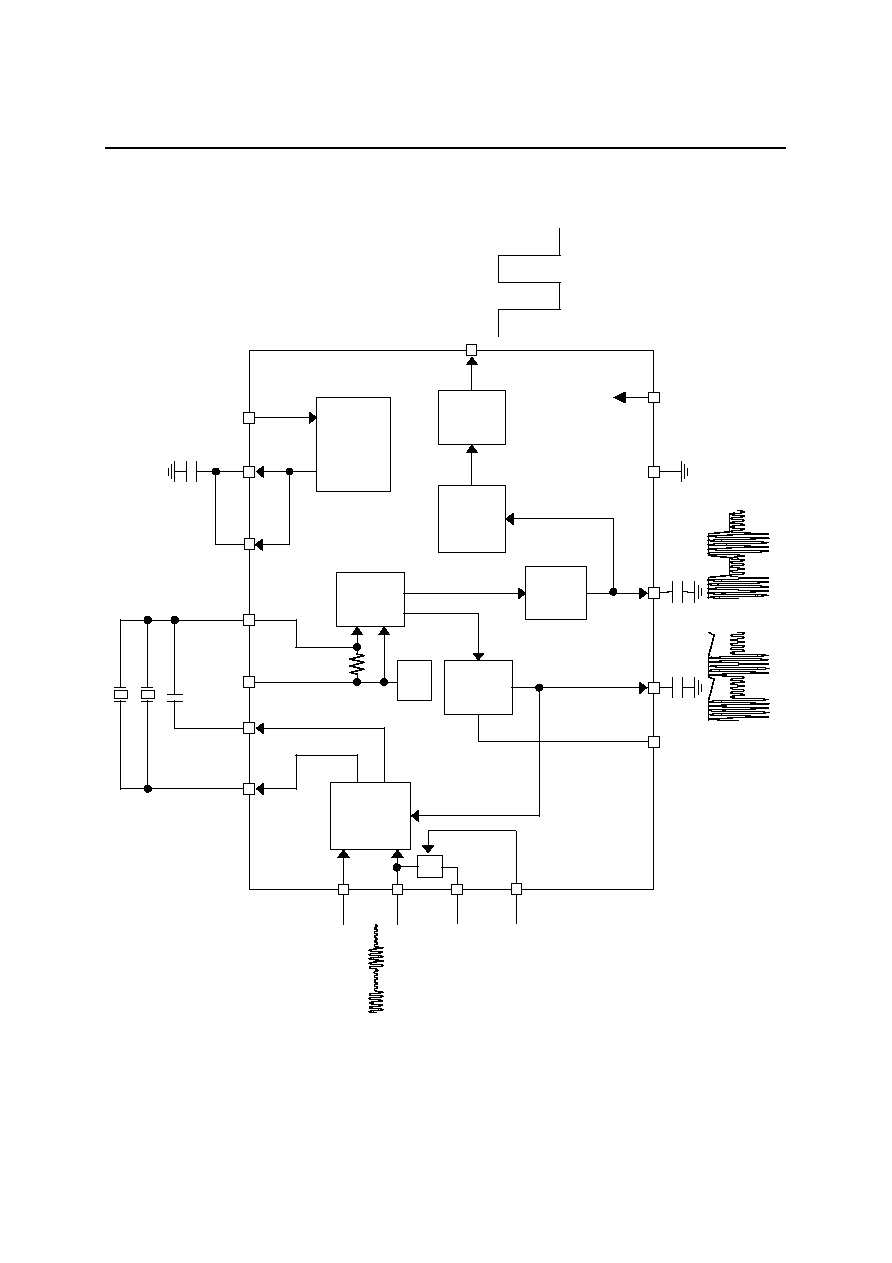
BLOCK DIAGRAM
PON
VR
E
G
AM
P
wi
t
h
AGC
AM
P
AGC
Re
c
t
ifi
e
r
REG
&
BI
AS
Sl
ic
e
r
Le
v
e
l
Sh
if
t
e
r
A
nt
e
n
na
In
pu
t
AGC DE
T
GND
VDD
T
C
O Ou
tp
u
t
AGC
HOL
D
IN
1
AG
CAM
P
OU
T
P
AG
CAM
P
OU
T
N
AM
P
INP
AM
P
INN
4.7
µ
F
+
80%
/-
20%
10
µ
F
+
80%
/-
20%
0.022
µ
F
+
80%
/-
20%
IN
2
CSW
2p
F
(
n
o
t
e)
BIAS
(
*
)
Use a cap
aci
t
o
r eq
u
a
l
t
o
t
h
e cap
aci
t
a
n
ce
b
e
t
w
een
t
h
e crys
t
a
l
p
i
n
s
.
+
+
SW
FSEL
VR
E
G
FEDL6190B-01
OKI Semiconductor
ML6190B
3/11
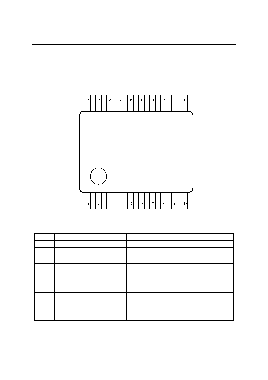
PIN SPECIFICATIONS
∑ Package
20-pin SSOP (0.65 mm pitch)
∑ Pin configuration
Pin Symbol
Function
Pin
Symbol
Function
1
VREG
Regulator output pin
11
AMPINP
AMP input pin
2 VDD
External power supply
pin
12
AMPINN
AMP input pin
3
GND
Ground pin
13
AGCAMPOUTN
AGCAMP output pin
4 FSEL
Antenna switch control
pin
14
AGCAMPOUTP
AGCAMP output pin
5
PON
Power-on input pin
15
GND
Ground pin
6
TCO
Time code output pin
16
VREG
Regulator output pin
7
AGC_HOLD
AGC hold input pin
17
GND
Ground pin
8 AGC
AGC pin for external
capacitor
18
CSW
Antenna input pin
9 DET
DET pin for external
capacitor
19
IN2
Antenna input pin
10
GND
Ground pin
20
IN1
Antenna input pin

FEDL6190B-01
OKI Semiconductor
ML6190B
4/11
∑ Pin descriptions
Pin Symbol
I/O
Description
1 VREG
--
Regulator output pin
Connect a 4.7
µ
F capacitor between this pin
and the GND pin.
Either polar or non-polar capacitors can be
used. When using polar capacitors, connect
them as shown in the block diagram.
This pin is connected to pin 16 internally but
should also be connected externally.
2
VDD --
External power supply pin
3
GND --
Ground pin
4 FSEL
I
Antenna switch control pin
5 PON
O
Power-on input pin
"H": Normal operation
"L": Standby operation
6 TCO
I
Time code output pin
The "H" output for the large amplitude signal,
the "L" output for the small amplitude signal,
and "H" output in the standby state.
7 AGC_HOLD
--
AGC hold input pin
"H": AGC operation
"L": AGC hold operation
8 AGC
--
AGC pin for an external capacitor
Connect a 10
µ
F capacitor between this pin
and the GND pin.
Either polar or non-polar capacitors can be
used. When using polar capacitors, connect
them as shown in the block diagram.
9 DET
DET pin for an external capacitor
Connect a 0.022
µ
F capacitor between this
pin and the GND pin.
10
GND --
Ground pin
11
AMPINP I
AMP input pin
12 AMPINN
I
AMP input pin
Leave this pin open.
13
AGCAMPOUTN O
Output pin for AMP with AGC
14
AGCAMPOUTP O
Output pin for AMP with AGC
15
GND --
Ground pin
16
VREG --
Regulator output pin
This pin is connected to pin 1 internally but
should also be connected externally.
17
GND --
Ground pin
18
CSW I
Antenna input pin
19
IN2 I
Antenna input pin
20
IN1 I
Antenna input pin
FEDL6190B-01
OKI Semiconductor
ML6190B
5/11
RADIO WAVE RECEIVING IC SPECIFICATIONS
Absolute Maximum Ratings
Parameter Symbol Condition
Rating Unit
Maximum supply voltage
V
DD
≠0.3 to +3.8
V
Input voltage
V
IN
Ta = 25
∞
C
≠0.3 to V
DD
+0.3 V
Operating temperature*
Top
--
≠40 to +85
∞
C
Storage temperature
T
STG
--
≠55 to +125
∞
C
*: The temperature that does not cause permanent damage to the device (Performance may not be guaranteed)
Recommended Operating Conditions
Parameter Symbol Condition
Rating Unit
Operating voltage
V
DD
--
1.1 to 3.6
V
Operating temperature
T
OP
--
≠25 to +85
∞
C
Electrical Characteristics
VDD = 1.5 V, GND = 0 V, Ta = 25
∞
C, f
IN
= 60 kHz, and modulation factor = 90 %, unless otherwise specified.
∑ DC characteristics
Parameter Symbol Condition
Min. Typ. Max. Unit
Supply current
I
DD
-- --
17
38
µ
A
Standby current
I
STB
-- --
--
0.01
µ
A
∑ AC characteristics
Parameter Symbol Condition
Min. Typ. Max. Unit
Voltage sensitivity
V
INmin
--
--
1.0
--
µ
Vrms
Maximum signal input
V
INmax
-- 100
--
--
mVrms
Between IN1 and IN2 pins
2
--
--
M
Input resistance
R
in
Between AMPINP and
AMPINN pins
500 k
Input capacitance
C
in
-- --
--
5
pF
Receiving frequency
f
IN
-- 40
--
100
kHz
∑ TCO output characteristics
Parameter Symbol Condition
Min. Typ. Max. Unit
Output voltage (high)
V
OH
-- V
DD
-
0.1
-- -- V
Output voltage (low)
V
OL
-- --
--
0.1
V
Output short current
(high)
I
OH
V
DD
= 3.6 V
V
O
= 0 V
--
-
36
--
µ
A
Output short current
(low)
I
OL
V
DD
= 3.6 V
V
O
= 3.6 V
-- 36 --
µ
A
Output pulse width
(500 ms input)
T
500
--
400 500 600 ms
Output pulse width
(800 ms input)
T
800
--
700 800 900 ms
Output pulse width
(200 ms input)
T
200
--
100 200 300 ms
FEDL6190B-01
OKI Semiconductor
ML6190B
6/11
∑ AGC hold characteristics
Parameter Symbol Condition
Min. Typ. Max. Unit
AGC_HOLD
"H" input voltage
V
IHAH
During normal operation
0.9*V
DD
--
-- V
AGC_HOLD
"L" input voltage
V
ILAH
During AGC hold
--
--
0.1*V
DD
V
AGC_HOLD
"H" input current
|I
IHAH
|
VI = V
DD
--
0.01
--
µ
A
AGC_HOLD
"L" input current
|I
ILAH
|
VI = 0.0V
--
0.01
--
µ
A
∑ PON characteristics
Parameter Symbol Condition
Min. Typ. Max. Unit
PON "H" input voltage
V
IHPON
During normal operation
0.9*V
DD
--
-- V
PON "L" input voltage
V
ILPON
During standby mode
-- --
0.1*V
DD
V
PON "H" input current
|I
IHPON
|
VI = V
DD
--
0.01
--
µ
A
PON "L" input current
|I
ILPON
|
VI = 0.0V
--
0.01
--
µ
A
∑ FSEL characteristics
Parameter Symbol Condition
Min. Typ. Max. Unit
FSEL "H" input voltage
V
IHFSEL
Antenna switch ON
0.9*V
DD
--
-- V
FSEL "L" input voltage
V
ILFSEL
Antenna switch OFF
-- --
0.1*V
DD
V
FSEL "H" input current |I
IHFSEL
|
VI = V
DD
--
0.01
--
µ
A
FSEL "L" input current
|I
ILFSEL
|
VI = 0.0V
--
0.01
--
µ
A
Switching ON
resistance
R
SWH
HSEL = "H"
350
--
--
k
Switching OFF
resistance
R
SWL
FSEL = "L"
--
20
100
∑ Delay characteristics
Parameter Symbol Condition
Min. Typ. Max. Unit
AGC setup time
T
AGC
At the time of PON
-- 3 --
sec
Response delay
T
TCO
Phase delay relative to
input signal
-- 50 --
ms

FEDL6190B-01
OKI Semiconductor
ML6190B
7/11
DESCRIPTION OF EACH BLOCK
(1) AMP Block
Radio waves received by the antenna will be amplified by AMP with AGC. Signals output from AMP with AGC
will go through an external quartz resonator, which serves as a band-pass filter, and will be amplified again at
AMP.
(2) AGC Block
Output signals from AMP will be input to the AGC block and the rectifier block. After signals are input to the
AGC block, their high side peak amplitudes are detected. As AGC signals, they will be fed back to AMP with
AGC.
The AGC block has the AGC hold function. When the AGC hold signal is "H," the block performs the regular
AGC operation. The AGC block performs the AGC hold operation when the AGC hold signal is "L."
(3) Rectifier Block
After signals are input to the rectifier block, their high side peak amplitudes are detected. As DET signals, they
will be transferred to the slicer block.
Crystal
AGC
AGC signal
(To AMP with AGC)
DET signal
(to slicer block)
Rectifier
AMP with
AGC
AMP
FEDL6190B-01
OKI Semiconductor
ML6190B
8/11
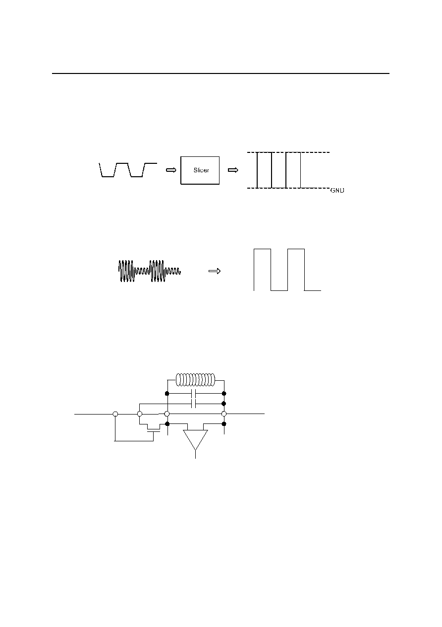
(4) Slicer Block
Signals output from the rectifier block are input to the slicer block and will be shaped to V
DD
as "1" and GND as
"0". Then, these outputs will be output as time codes (TCO).
This LSI has the standby function. When the PON signal is "H," the LSI will perform the regular operation. When
the PON signal is "L," the LSI will be in standby state. The TCO during the standby state is "H."
(5) Time Code Output
The time code output (TCO) of the ML6190B is in phase with actual time codes input from the antenna. A "H"
level is output for the large amplitude signal and a "L" level is output for the small amplitude signal.
(6) Connecting the Antenna
The ML6190B has a built-in antenna switch to allow reception of two receive frequencies. When receiving only
one frequency, connect both the antenna and C1 across IN1 and IN2. When receiving two frequencies, add C2
across CSW and IN1 to enable frequency switching.
40 kHz/60 kHz Antenna Connection Example
Antenna Input Signal
Time Code Output (TCO)
VDD
C1
C2
IN2
IN1
CSW
FSEL

FEDL6190B-01
OKI Semiconductor
ML6190B
9/11
PACKAGE DIMENSIONS
SSOP20-P-44-0.65-K
Mirror Finish
Package material
Epoxy resin
Lead frame material
42 alloy
Pin treatment
Solder plating (
5µm)
Package weight (g)
0.088 TYP.
5
Rev. No./Last Revised
1/Jan. 22, 1999
Notes for Mounting the Surface Mount Type Package
The surface mount type packages are very susceptible to heat in reflow mounting and humidity absorbed in storage.
Therefore, before you perform reflow mounting, contact Oki's responsible sales person for the product name,
package name, pin number, package code and desired mounting conditions (reflow method, temperature and
times).
(Unit: mm)
FEDL6190B-01
OKI Semiconductor
ML6190B
10/11
REVISION HISTORY
Page
Document No.
Date
Previous
Edition
Current
Edition
Description
PEDL6190B-01
Jan. 7, 2005
≠
≠
Preliminary edition 1
≠
≠
Final edition 1
1 1
Modified contents in the "GENERAL
DESCRIPTION" Section.
2 2
Modified the block diagram and eliminated
"Note".
4 4
Partially added contents of the descriptions of
Pins 1, 8, and 16.
FEDL6190B-01
Mar. 3, 2005
5, 6
5, 6
Partially changed contents in the "Electrical
characteristics" Section.

FEDL6190B-01
OKI Semiconductor
ML6190B
11/11
NOTICE
1. The information contained herein can change without notice owing to product and/or technical improvements.
Before using the product, please make sure that the information being referred to is up-to-date.
2. The outline of action and examples for application circuits described herein have been chosen as an explanation
for the standard action and performance of the product. When planning to use the product, please ensure that the
external conditions are reflected in the actual circuit, assembly, and program designs.
3. When designing your product, please use our product below the specified maximum ratings and within the
specified operating ranges including, but not limited to, operating voltage, power dissipation, and operating
temperature.
4. Oki assumes no responsibility or liability whatsoever for any failure or unusual or unexpected operation
resulting from misuse, neglect, improper installation, repair, alteration or accident, improper handling, or
unusual physical or electrical stress including, but not limited to, exposure to parameters beyond the specified
maximum ratings or operation outside the specified operating range.
5. Neither indemnity against nor license of a third party's industrial and intellectual property right, etc. is granted
by us in connection with the use of the product and/or the information and drawings contained herein. No
responsibility is assumed by us for any infringement of a third party's right which may result from the use
thereof.
6. The products listed in this document are intended for use in general electronics equipment for commercial
applications (e.g., office automation, communication equipment, measurement equipment, consumer
electronics, etc.). These products are not, unless specifically authorized by Oki, authorized for use in any
system or application that requires special or enhanced quality and reliability characteristics nor in any system
or application where the failure of such system or application may result in the loss or damage of property, or
death or injury to humans.
Such applications include, but are not limited to, traffic and automotive equipment, safety devices, aerospace
equipment, nuclear power control, medical equipment, and life-support systems.
7. Certain products in this document may need government approval before they can be exported to particular
countries. The purchaser assumes the responsibility of determining the legality of export of these products and
will take appropriate and necessary steps at their own expense for these.
8. No part of the contents contained herein may be reprinted or reproduced without our prior permission.
Copyright 2005 Oki Electric Industry Co., Ltd.