
PEDL66517-03
1Semiconductor
This version: Nov. 1999
Previous version: Aug. 1999
ML66517 Family
Preliminary
16-Bit Microcontroller
1/28
GENERAL DESCRIPTION
The ML66517 family of highly functional CMOS 16-bit single chip microcontrollers utilizes the nX-8/500S, Oki's
proprietary CPU core.
Each device includes capture input with an internal digital filter, 10-bit A/D converter, a number of timers, and
dedicated 3-phase PWM (6 outputs) function capable of generating and controlling of AC/DC motor driving
waveforms.
By means of the internal dedicated function for motor control, this general-purpose microcontroller is optimally
suited for DC and AC motor control applications for energy saving. And the internal hardware multiplier allows
high-speed arithmetic operations to be executed. And also the internal clock multiplication circuit can reduce the
source frequency noise so that high-speed operations can be performed.
The flash ROM versions (ML66Q517 and ML66Q515) programmable with a single 5V power supply are also
included in the family. These versions are easily adaptable to quick specification changes and to new product
versions.
APPLICATIONS
Air conditioner or inverter control
Motor control for FA equipment
ORDERING INFORMATION
Order Code or Product Name
Package
Remark
ML66514-RB
5 V mask ROM version
ML66Q515-RB
80-pin plastic QFP
(QFP 80-P-1420-0.80-BK)
5 V flash ROM version
ML66517-GA
5 V mask ROM version
ML66Q517-GA
64-pin plastic SDIP
(SDIP 64-P-750-1.778)
MSM66517 flash ROM version
PEDL66517-03
1Semiconductor
ML66517 Family
2/28
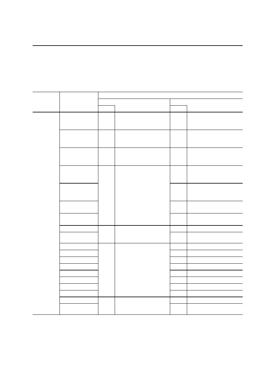
FEATURES
Name
ML66514
ML66517
Operating temperature
�40�C to 85�C
Power supply voltage/
Maximum frequency
V
DD
= 4.5 to 5.5 V/f = 25 MHz
Minimum instruction
execution time
80 nsec @25 MHz
Internal ROM size
(max. external)
32 KB (64 KB)
64 KB (128 KB)
Internal RAM size
(max. external)
1 KB (64 KB)
2 KB (64 KB)
I/O ports
46 I/O pins (with pull-up resistors,
programmable at the bit level),
4 input pins
56 I/O pins (with pull-up resistors,
programmable at the bit level),
8 input pins
16-bit free-running counter
�
1ch
Compare output/capture input
�
2ch
16-bit timer (auto-reload/timer out)
�
1ch
8-bit auto reload timer
�
2ch
8-bit auto reload timer
�
4ch (can
also be used as 16-bit auto reload
timer
�
1ch and 8-bit auto reload
timer
�
2ch)
Capture
�
2ch
8-bit auto reload timer
�
2ch
(also functions as serial communication baud rate generators)
8-bit auto reload timer
�
1ch (also functions as a watchdog timer)
Timers
8-bit PWM
�
2ch (can also be used as
16-bit PWM
�
1ch)
8-bit PWM
�
4ch (can also be used
as 16-bit PWM
�
2ch)
Serial port
Synchronous/UART
�
2ch
A/D converter
10-bit
�
4ch
10-bit
�
8ch
3-phase PWM (AC motor control)
Available
3-phase PWM (DC motor control)
Available
External interrupt
Non-Maskable
�
1ch
Maskable
�
2ch
Non-Maskable
�
1ch
Maskable
�
4ch
Interrupt priority
3 levels
Multiplexed address and data buses
Others
Multiplication calculator
Flash ROM version
ML66Q515
(ROM = 64 KB, RAM = 2 KB)
ML66Q517

PEDL66517-03
1Semiconductor
ML66517 Family
3/28
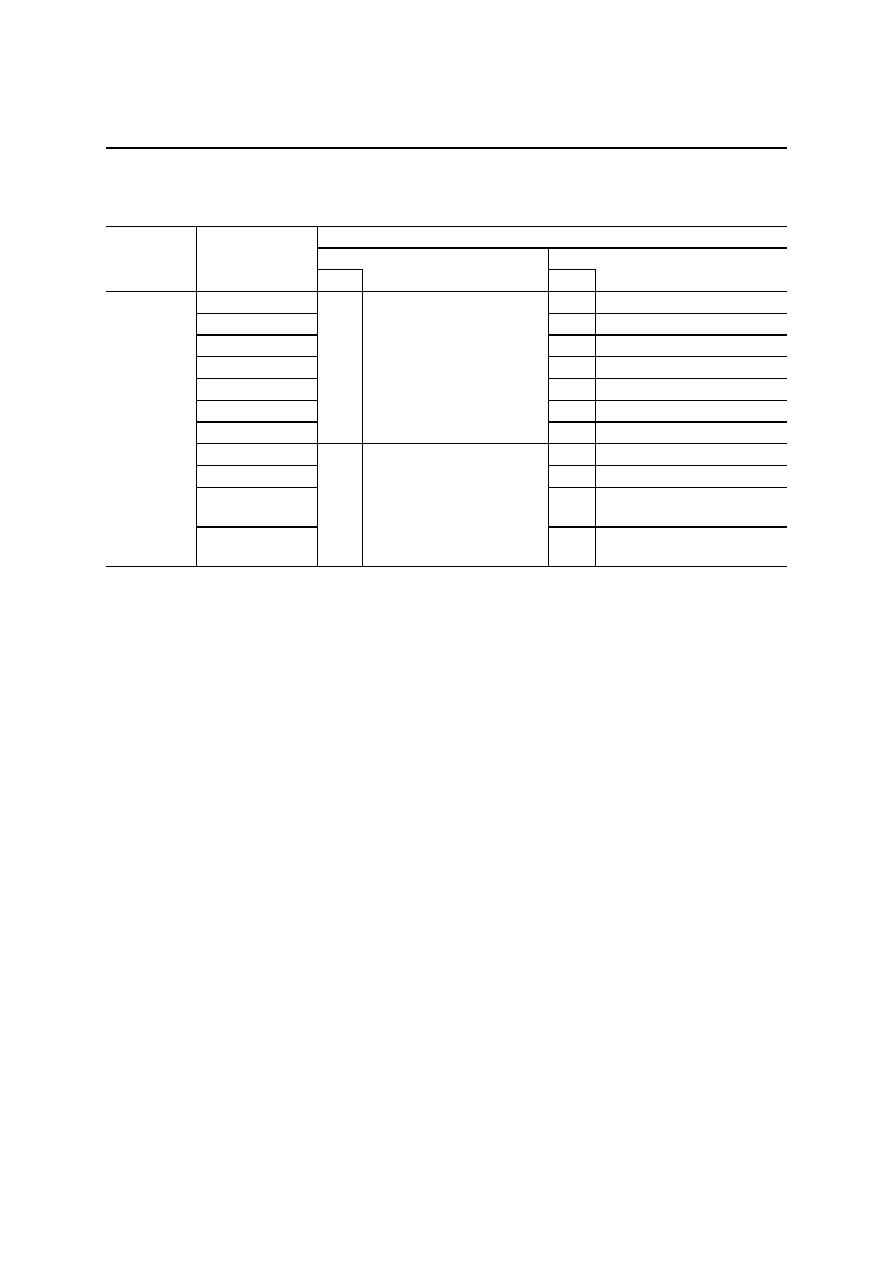
SPECIAL FEATURES
1. High-performance CPU
The family includes the high-performance CPU, powerful bit manipulation instruction set, full symmetrical
addressing mode, and ROM WINDOW function, and also provides the best optimized C compiler support.
2. 3-phase PWM circuit for generating motor drive waveforms
The device includes a 16-bit three-phase PWM (six outputs) circuit designed specifically for generating AC
three-phase motor or DC three-phase brushless motor drive waveforms. PWM and level outputs can be switched
by compare and match circuitry and software, and the compare and match circuitry can switch the outputs in real
time.
The device has circuitry to fix the three-phase outputs at an inactive level by inputting malfunction signals from a
motor at the specific pin.
3. Capture inputs with digital filter filters
The device has two channels of capture inputs with 3/4 digital filters. The device is best suited to event interval
measurement, pulse width measurement, etc. in a high noise environment such as motor control. An optimum
filter can be selected according to noise width since a sampling interval of an input signal can be selected. A digital
filter OFF mode can also be selected.
4. High-speed multiplier
The device includes a dedicated high-speed multiplier.
The calculation time, 16 bits � 16 bits = 32 bits, is 200 ns (f = 25 MHz).
5. Clock multiplication circuit
The device includes a clock multiplication circuit in which the clock can be selected as a source clock (PLL OFF),
1 � clock, 2 � clock, or 4 � clock.
Therefore, the use of a low frequency oscillator (external clock) allows the device to internally operate at a high
speed, which achieves noise reduction and lower power consumption.
6. Flash memory version programmable with a single power supply
In addition to the mask ROM versions, the family includes the versions (ML66Q517 and ML66Q515) with 64 KB
flash memory that can be programmed with a single 5 V supply.
7. A high-precision A/D converter
The device has a high precision 10-bit A/D converter with eight channels.
An independent result register for each channel provides easy accessibility by software.
The A/D converter is activated in a channel select mode, and automatic conversion is also implemented in a scan
mode which scans from any designated channel to the last channel (ch 7).
8. Programmable pull-up resistors
Building the pull-up resistors into the chip contributes to overall design compactness. Making them
programmable on a per-bit basis allows complete flexibility in circuit board layout and system design. These
programmable pull-up resistors are available for all I/O pins not already assigned specific functions (such as the
oscillator connection pins).

PEDL66517-03
1Semiconductor
ML66517 Family
4/28
PWM output switching every 60
�
�
�
�
of motor turn using the compare-out timer
PWM Output Timing (DC Motor Control)
PWM Output Timing (AC Motor Control)
PWM-U
PWM-UB
PWM-V
PWM-VB
PWM-W
PWM-WB
CAP input
Compare register
value setting
Compare-match
generation
CAP input
Period register
setting value
16-bit counter value
0000H
PWM-U
(U)
PWM-UB
(
U
)
Underflow counts up the counter
Set by 8-bit dead-time timer
(Only U and
U
output signals are indicated above)

PEDL66517-03
1Semiconductor
ML66517 Family
5/28
BLOCK DIAGRAM
16-bit Timer0
ALU
Memory Control
Pointing Registers
Local Registers
Instruction
Decoder
RAM 2K
8-bit Timer6/WDT
Bus Port Control
System
Control
CPU Core
TM0OUT
TM0EVT
RES
CLKSEL1
CLKSEL0
OSC1
OSC0
EA
PSEN
WR
RD
ALE
3-phase
PWM
INACT
PWMVB
CAP
ROM
64K
A8 to A16
AD0 to AD7
Port Control
P0
P1
P2
P3
P5
P6
P7
P8
P10
P11
P12
TBC
SSP
Control
Registers
LRB
PSW
PC
CSR
TSR
ALU Control
ACC
10-bit A/D
Converter
V
REF
AGND
AI0 to AI7
Interrupt
NMI
EXINT0
EXINT3
to
P15
P16
P17
Peripheral
8-bit Timer9
8-bit Timer4/BRG
8-bit Timer3/BRG
TM5EVT
8-bit Timer5
CLKOUT
TM1OUT
TM1EVT
TM2EVT
SIO6
(UART/SYNC)
RXD6
TXD6
RXC6
SIO1
(UART/SYNC)
RXD1
RXC1
TXC1
TXD1
8-bit PWM0
PWM0OUT
PWM2OUT
PWM1OUT
PWM3OUT
8-bit PWM1
8-bit Timer1
8-bit Timer2
TM2OUT
TXC6
PWMV
PWMW
PWMWB
PWMUB
PWMU
CAP/CMP
16-bit FRC
CMP
CAPF0
CAPF1
CPCMF0
CPCMF1
ML66517/ML66Q517 Block Diagram
PEDL66517-03
1Semiconductor
ML66517 Family
6/28
16-bit Timer0
ALU
Memory Control
Pointing Registers
Local Registers
Instruction
Decoder
RAM
1K/2K
8-bit Timer6/WDT
Bus Port Control
System
Control
CPU Core
TM0OUT
TM0EVT
RES
CLKSEL1
CLKSEL0
OSC1
OSC0
EA
PSEN
WR
RD
ALE
ROM
32K/64K
A8 to A15
AD0 to AD7
Port Control
P0
P1
P3
P5
P6
P7
P8
P11
P12
TBC
SSP
Control
Registers
LRB
PSW
PC
ALU Control
ACC
P15
P16
P17
3-phase
PWM
INACT
PWMVB
CAP
10-bit A/D
Converter
V
AGND
AI4 to AI7
Interrupt
NMI
EXINT0
EXINT1
REF
to
Peripheral
8-bit Timer9
8-bit Timer4/BRG
8-bit Timer3/BRG
8-bit Timer5
CLKOUT
SIO6
(UART/SYNC)
RXD6
TXD6
RXC6
SIO1
(UART/SYNC)
RXD1
RXC1
TXC1
TXD1
8-bit PWM0
PWM0OUT
PWM1OUT
8-bit PWM1
TXC6
PWMV
PWMW
PWMWB
PWMUB
PWMU
CAP/CMP
16-bit FRC
CMP
CAPF0
CAPF1
CPCMF0
CPCMF1
*1
*2
*1 ML66Q515 has 2KB RAM, ML66514 has 1KB RAM
*2 ML66Q515 has 64KB ROM, ML66514 has 32KB ROM
ML66Q515/ML66514 Block Diagram
PEDL66517-03
1Semiconductor
ML66517 Family
7/28
PIN CONFIGURATION (TOP VIEW)
TXC1/P8-3
PWM2OUT/P8-6
PWM3OUT/P8-7
PWM0OUT/P7-6
PWM1OUT/P7-7
V
DD
GND
PWMU/P16-0
PWMUB/P16-1
PWMV/P16-2
PWMVB/P16-3
PWMW/P16-4
PWMWB/P16-5
INACT/P16-6
NMI
CAPF0/P17-0
CAPF1/P17-1
CPCMF0/P17-2
CPCMF1/P17-3
EXINT0/P6-0
EXINT1/P6-1
P1-6/A14
P1-5/A13
P1-4/A12
P1-3/A11
P1-2/A10
P1-1/A9
P1-0/A8
GND
P3-3/WR
P3-2/RD
P3-1/PSEN
P3-0/ALE
P0-7/AD7
P0-6/AD6
P0-5/AD5
P0-4/AD4
P0-3/AD3
P0-2/AD2
P0-1/AD1
P0-0/AD0
EA
RES
CLKSEL1
CLKSEL0
V
DD
OSC1
OSC0
GND
P11-2/CLKOUT
P10-7/TM5EVT
P5-7/TM0EVT
P5-6/TM0OUT
P6-7/TM2OUT
P6-6/TM2EVT
P6-5/TM1OUT
P6-4/TM1EVT
P6-3/EXINT3
P6-2/EXINT2
V
DD
V
REF
AI0/P12-0
AI1/P12-1
AI2/P12-2
AI3/P12-3
AI4/P12-4
AI5/P12-5
AI6/P12-6
AI7/P12-7
AGND
GND
RXD6/P15-0
TXD6/P15-1
RXC6/P15-2
TXC6/P15-3
RXD1/P8-0
TXD1/P8-1
RXC1/P8-2
65
70
75
80
1
5
10
15
20
60
55
50
45
40
35
30
25
P1-7/A15
P2-0/A16
80-Pin Plastic QFP
ML66517/ML66Q517 Pin Configuration
PEDL66517-03
1Semiconductor
ML66517 Family
8/28
TXC1/P8-3
PWM0OUT/P7-6
PWM1OUT/P7-7
PWMU/P16-0
PWMUB/P16-1
PWMV/P16-2
PWMVB/P16-3
PWMW/P16-4
PWMWB/P16-5
INACT/P16-6
NMI
CAPF0/P17-0
CAPF1/P17-1
P1-3/A11
P1-2/A10
P1-1/A9
P1-0/A8
GND
P3-3/WR
P3-2/RD
P3-1/PSEN
P3-0/ALE
P0-7/AD7
P0-6/AD6
P0-5/AD5
P0-4/AD4
P0-3/AD3
P0-2/AD2
P0-1/AD1
P0-0/AD0
EA
RES
CLKSEL1
CLKSEL0
V
DD
OSC1
OSC0
GND
P11-2/CLKOUT
P5-7/TM0EVT
P5-6/TM0OUT
P6-1/EXINT1
P6-0/EXINT0
P17-3/CPCMF1
P17-2/CPCMF0
A12/P1-4
A13/P1-5
A14/P1-6
A15/P1-7
V
DD
V
REF
AI4/P12-4
AI5/P12-5
AI6/P12-6
AI7/P12-7
AGND
GND
RXD6/P15-0
TXD6/P15-1
RXC6/P15-2
TXC6/P15-3
RXD1/P8-0
TXD1/P8-1
RXC1/P8-2
49
60
64
1
10
48
40
33
17
30
64-Pin Plastic QFP
ML66Q515/ML66514 Pin Configuration

PEDL66517-03
1Semiconductor
ML66517 Family
9/28
PSEN/P3-1
P3-0/ALE
P0-7/AD7
P0-6/AD6
P0-5/AD5
P0-4/AD4
P0-3/AD3
P0-2/AD2
P0-1/AD1
P0-0/AD0
EA
RES
CLKSEL1
CLKSEL0
V
DD
OSC1
OSC0
GND
P11-2/CLKOUT
P5-7/TM0EVT
P5-6/TM0OUT
P6-1/EXINT1
P6-0/EXINT0
P17-3/CPCMF1
P17-2/CPCMF0
P17-1/CAPF1
P17-0/CAPF0
NMI
P16-6/INACT
P16-5/PWMWB
P16-4/PWMW
P16-3/PWMVB
P16-2/PWMV
RD/P3-2
WR/P3-3
GND
A8/P1-0
A9/P1-1
A10/P1-2
A11/P1-3
A12/P1-4
A13/P1-5
A14/P1-6
A15/P1-7
V
DD
V
REF
AI4/P12-4
AI5/P12-5
AI6/P12-6
AI7/P12-7
AGND
GND
RXD6/P15-0
TXD6/P15-1
RXC6/P15-2
TXC6/P15-3
RXD1/P8-0
TXD1/P8-1
RXC1/P8-2
TXC1/P8-3
PWM0OUT/P7-6
PWM1OUT/P7-7
PWMU/P16-0
PWMUB/P16-1
64-Pin Plastic SDIP
ML66Q515/ML66514 Pin Configuration
PEDL66517-03
1Semiconductor
ML66517 Family
10/28
PIN DESCRIPTIONS
In the Type column, "I" indicates an input pin, "O" indicates an output pin, and "I/O" indicates an I/O pin.
ML66517/ML66Q517 Pin Descriptions
Description
Function
Symbol
Type
Primary function
Type
Secondary function
P0_0/AD0
to
P0_7/AD7
I/O
8-bit I/O port
Pull-up resistors can be
specified for each individual bit
I/O
External memory access
Address output/data I/O port
P1_0/A8
to
P1_7/A15
I/O
8-bit I/O port
Pull-up resistors can be
specified for each individual bit
O
External memory access
Address output port
P2_0/A16
I/O
1-bit I/O port
Pull-up resistors can be
specified for each individual bit
O
External memory access
Address output port
P3_0/ALE
O
External memory access
Address latch enable signal
output pin
P3_1/
PSEN
O
External program memory
access
Read strobe output pin
P3_2/
RD
O
External memory access
Read strobe output pin
P3_3/
WR
I/O
4-bit I/O port
10 mA sink capability
Pull-up resistors can be
specified for each individual bit
O
External memory access
Write strobe output pin
P5_6/TM0OUT
O
Timer 0 timer output pin
P5_7/TM0EVT
I/O
2-bit I/O port
Pull-up resistors can be
specified for each individual bit
I
Timer 0 external event input pin
P6_0/EXINT0
I
External interrupt 0 input pin
P6_1/EXINT1
I
External interrupt 1 input pin
P6_2/EXINT2
I
External interrupt 2 input pin
P6_3/EXINT3
I
External interrupt 3 input pin
P6_4/TM1EVT
I
Timer 1 external event input pin
P6_5/TM1OUT
O
Timer 1 timer output pin
P6_6/TM2EVT
I
Timer 2 external event input pin
P6_7/TM2OUT
I/O
8-bit I/O port
Pull-up resistors can be
specified for each individual bit
O
Timer 2 timer output pin
P7_6/PWM0OUT
O
PWM0 output pin
Port
P7_7PWM1OUT
I/O
2-bit I/O port
Pull-up resistors can be
specified for each individual bit
O
PWM1 output pin

PEDL66517-03
1Semiconductor
ML66517 Family
11/28
ML66517/ML66Q517 Pin Descriptions (Continued)
Description
Function
Symbol
Type
Primary function
Type
Secondary function
P8_0/RXD1
I
SIO1 receive data input pin
P8_1/TXD1
O
SIO1 transmit data output pin
P8_2/RXC1
I/O
SIO1 receive clock I/O pin
P8_3/TXC1
I/O
SIO1 transmit clock I/O pin
P8_6/PWM2OUT
O
PWM2 output pin
P8_7PWM3OUT
I/O
6-bit I/O port
Pull-up resistors can be
specified for each individual bit
O
PWM3 output pin
P10_7/TM5EVT
I/O
1-bit I/O port
Pull-up resistors can be
specified
I
Timer 5 external event input pin
P11_2/CLKOUT
I/O
1-bit I/O port
Pull-up resistors can be
specified
O
Main clock pulse output pin
P12_0/AI0
to
P12_7/AI7
I
8-bit input port
I
A/D converter analog input port
P15_0/RXD6
I
SIO6 receive data input pin
P15_1/TXD6
O
SIO6 transmit data output pin
P15_2/RXC6
I/O
SIO6 receive clock I/O pin
P15_3/TXC6
I/O
4-bit I/O port
Pull-up resistors can be
specified for each individual bit
I/O
SIO6 transmit clock I/O pin
P16_0/PWMU
O
3-phase PWMU output pin
P16_1/PWMUB
O
3-phase PWMUB output pin
P16_2/PWMV
O
3-phase PWMV output pin
P16_3/PWMVB
O
3-phase PWMVB output pin
P16_4/PWMW
O
3-phase PWMW output pin
P16_5/PWMWB
O
3-phase PWMWB output pin
P16_6/
INACT
I/O
7-bit I/O port
Pull-up resistors can be
specified for each individual bit
I
Abnormality detect input pin
P17_0/CAPF0
I
Capture 0 input pin
P17_1/CAPF1
I
Capture 1 input pin
P17_2/CPCMF0
I/O
Capture 0 input/compare 0 output
pin
Port
P17_3/CPCMF1
I/O
4-bit I/O port
Pull-up resistors can be
specified for each individual bit
I/O
Capture 1 input/compare 1 output
pin

PEDL66517-03
1Semiconductor
ML66517 Family
12/28
ML66517/ML66Q517 Pin Descriptions (Continued)
Function
Symbol
Type
Description
V
DD
I
Power supply pin
Connect all V
DD
pins to the power supply.*
GND
I
GND pin
Connect all GND pins to GND.*
V
REF
I
Analog reference voltage pin
Power
supply
AGND
I
Analog GND pin
OSC0
I
Main clock oscillation input pin
Connect to a crystal or ceramic oscillator. Or, input an external clock.
OSC1
O
Main clock oscillation output pin
Connect to a crystal or ceramic oscillator.
The clock output is opposite in phase to OSC0.
Leave this pin unconnected when an external clock is used.
CLKSEL0
I
Oscillation
CLKSEL1
I
Clock multiplication factor select pin
Clock multiplication factor is selected from source oscillation (PLL
OFF), source oscillation
�
2, or source oscillation
�
4
Reset
RES
I
Reset input pin
NMI
I
Non-maskable interrupt input pin
Others
EA
I
External program memory access input pin
If the
EA
pin is enabled (low level), the internal program memory is
masked and the CPU executes the program code in external program
memory all address space.
* Each of the family devices has unique pattern routes for the internal power and ground. Connect the
power supply voltage to all V
DD
pins and the ground potential to all GND pins. If a device may have
one or more V
DD
or GND pins to which the power supply voltage or the ground potential is not
connected, it can not be guaranteed for normal operation.

PEDL66517-03
1Semiconductor
ML66517 Family
13/28
ML66Q515/ML66514 Pin Descriptions
Description
Function
Symbol
Type
Primary function
Type
Secondary function
P0_0/AD0
to
P0_7/AD7
I/O
8-bit I/O port
Pull-up resistors can be
specified for each individual bit
I/O
External memory access
Address output/Data I/O port
P1_0/A8
to
P1_7/A15
I/O
8-bit I/O port
Pull-up resistors can be
specified for each individual bit
O
External memory access
Address output port
P3_0/ALE
O
External memory access
Address latch enable signal
output pin
P3_1/
PSEN
O
External program memory
access
Read strobe output pin
P3_2/
RD
O
External memory access
Read strobe output pin
P3_3/
WR
I/O
4-bit I/O port
10mA sink capability
Pull-up resistors can be
specified for each individual bit
O
External memory access
Write strobe output pin
P5_6/TIM0OUT
O
Timer 0 timer output pin
P5_7/TIM0EVT
I/O
2-bit I/O port
Pull-up resistors can be
specified for each individual bit
I
Timer 0 external event input pin
P6_0/EXINT0
I
External interrupt 0 input pin
P6_1/EXINT1
I/O
2-bit I/O port
Pull-up resistors can be
specified for each individual bit
I
External interrupt 1 input pin
P7_6/PWM0OUT
O
PWM0 output pin
P7_7/PWM1OUT
I/O
2-bit I/O port
Pull-up resistors can be
specified for each individual bit
O
PWM1 output pin
P8_0/RXD1
I
SIO1 receive data input pin
P8_1/TXD1
O
SIO1 transmit data output pin
P8_2/RXC1
I/O
SIO1 receive clock I/O pin
P8_3/TXC1
I/O
4-bit I/O port
Pull-up resistors can be
specified for each individual bit
I/O
SIO1 transmit clock I/O pin
P11_2/CLKOUT
I/O
1-bit I/O port
Pull-up resistors can be
specified
O
Main clock pulse output pin
P12_4/AI4
to
P12_7/AI7
I
4-bit input port
I
A/D converter analog input port
P15_0/RXD6
I
SIO6 receive data input pin
P15_1/TXD6
O
SIO6 transmit data output pin
P15_2/RXC6
I/O
SIO6 receive clock I/O pin
Port
P15_3/TXC6
I/O
4-bit I/O port
Pull-up resistors can be
specified for each individual bit
I/O
SIO6 transmit clock I/O pin
PEDL66517-03
1Semiconductor
ML66517 Family
14/28
ML66Q515/ML66514 Pin Descriptions (Continued)
Description
Function
Symbol
Type
Primary function
Type
Secondary function
P16_0/PWMU
O
3-phase PWMU output pin
P16_1/PWMUB
O
3-phase PWMUB output pin
P16_2/PWMV
O
3-phase PWMV output pin
P16_3/PWMVB
O
3-phase PWMVB output pin
P16_4/PWMW
O
3-phase PWMW output pin
P16_5/PWMWB
O
3-phase PWMWB output pin
P16_6/
INACT
I/O
7-bit I/O port
Pull-up resistors can be
specified for each individual
bit
I
Abnormality detect input pin
P17_0/CAPF0
I
Capture 0 input pin
P17_1/CAPF1
I
Capture 1 input pin
P17_2/CPCMF0
I/O
Capture 0 input/compare 0
output pin
Port
P17_3/CPCMF1
I/O
4-bit I/O port
Pull-up resistors can be
specified for each individual
bit
I/O
Capture 1 input/compare 1
output pin

PEDL66517-03
1Semiconductor
ML66517 Family
15/28
ML66Q515/ML66514 Pin Descriptions (Continued)
Function
Symbol
Type
Description
V
DD
I
Power supply pin
Connect all V
DD
pins to the power supply.*
GND
I
GND pin
Connect all GND pins to GND.*
V
REF
I
Analog reference voltage pin
Power supply
AGND
I
Analog GND pin
OSC0
I
Main clock oscillation input pin
Connect to a crystal or ceramic oscillator. Or, input an external
clock.
OSC1
O
Main clock oscillation output pin
Connect to a crystal or ceramic oscillator.
The clock output is opposite in phase to OSC0.
Leave this pin unconnected when an external clock is used.
CLKSEL0
I
Oscillation
CLKSEL1
I
Clock multiplication factor select pin
Clock multiplication factor is selected from source oscillation (PLL
OFF), source oscillation
�
2, or source oscillation
�
4
Reset
RES
I
Reset input pin
NMI
I
Non-maskable interrupt input pin
Others
EA
I
External program memory access input pin
If the
EA
pin is enabled (low level), the internal program memory is
masked and the CPU executes the program code in external
program memory all address space.
* Each of the family devices has unique pattern routes for the internal power and ground. Connect the
power supply voltage to all V
DD
pins and the ground potential to all GND pins. If a device may have
one or more V
DD
or GND pins to which the power supply voltage or the ground potential is not
connected, it can not be guaranteed for normal operation.

PEDL66517-03
1Semiconductor
ML66517 Family
16/28
ABSOLUTE MAXIMUM RATINGS
Parameter
Symbol
Condition
Rating
Unit
Digital power supply voltage
V
DD
�0.3 to +7.0
V
Input voltage
V
I
�0.3 to V
DD
+0.3
V
Output voltage
V
O
�0.3 to V
DD
+0.3
V
Analog reference voltage
V
REF
�0.3 to V
DD
+0.3
V
Analog input voltage
V
AI
GND = AGND = 0 V
Ta = 25�C
�0.3 to V
REF
V
80-pin QFP
600
64-pin QFP
520
Power dissipation
P
D
Ta = 85�C
per package
64-pin SDIP
1280
mW
Storage temperature
T
STG
--
�50 to +150
�C
RECOMMENDED OPERATING CONDITIONS
Parameter
Symbol
Condition
Range
Unit
Digital power supply voltage
V
DD
f
OSC
25 MHz
4.5 to 5.5
V
Analog reference voltage
V
REF
--
V
DD
� 0.3 to V
DD
V
Analog input voltage
V
AI
--
AGND to V
REF
V
Memory hold voltage
V
DDH
f
OSC
= 0 Hz
2.0 to 5.5
V
PLL (multiplier) OFF
2 to 25
Internal operating frequency
f
OSC
PLL (multiplier) ON
20 to 25
MHz
Ambient temperature
Ta
--
�40 to +85
�C
MOS load
20
--
P3
6
P0, P16
2
Fan out
N
TTL load
P1, P2, P5 to
P8, P10, P11,
P15, P17
1
--

PEDL66517-03
1Semiconductor
ML66517 Family
17/28
ALLOWABLE OUTPUT CURRENT
(1) ML66517/ML66Q517 (80-pin QFP)
(V
DD
= 4.5 to 5.5 V, Ta = �40 to +85�C)
Parameter
Pin
Symbol
Min.
Typ.
Max.
Unit
"H" output pin (1 pin)
All input pins
I
OH
--
--
�2
"H" output pins
(sum total)
Sum total of all output pins
IOH
--
--
�50
P3
--
--
10
"L" output pin (1 pin)
Other ports
I
OL
--
--
5
Sum total of P0, P3
60
Sum total of P1, P2
Sum total of P7, P8, P15
Sum total of P5, P6, P10,
P11, P16, P17
50
"L" output pins
(sum total)
Sum total of all output pins
IOL
--
--
100
mA
(2) ML66Q515/ML66514 (64-pin QFP/SDIP)
(V
DD
= 4.5 to 5.5 V, Ta = �40 to +85�C)
Parameter
Pin
Symbol
Min.
Typ.
Max.
Unit
"H" output pin (1 pin)
All input pins
I
OH
--
--
�2
"H" output pins
(sum total)
Sum total of all output pins
IOH
--
--
�20
P3
--
--
10
"L" output pin (1 pin)
Other ports
I
OL
--
--
5
Sum total of P0, P3
50
P1
Sum total of P5 to P8,
P11, P15, P17
30
"L" output pins
(sum total)
Sum total of all output pins
IOL
--
--
60
mA
Note: Each of the family devices has unique pattern routes for the internal power and ground. Connect
the power supply voltage to all V
DD
pins and the ground potential to all GND pins. If a device may
have one or more V
DD
or GND pins to which the power supply voltage or the ground potential is
not connected, it can not be guaranteed for normal operation.
PEDL66517-03
1Semiconductor
ML66517 Family
18/28
ELECTRICAL CHARACTERISTICS
DC Characteristics
(V
DD
= 4.5 to 5.5 V, Ta = �40 to +80�C)
Parameter
Symbol
Condition
Min.
Typ.
Max.
Unit
"H" input voltage
*1
0.44 V
DD
--
V
DD
+ 0.3
"H" input voltage
*2 to *8
V
IH
--
0.80 V
DD
--
V
DD
+ 0.3
"L" input voltage
*1
�0.3
--
0.16 V
DD
"L" input voltage
*2 to *8
V
IL
--
�0.3
--
0.2 V
DD
I
O
= �400 �A
V
DD
� 0.4
--
"H" output voltage
*1, *4, *5
I
O
= �2.0 mA
V
DD
� 0.6
--
--
I
O
= �200 �A
V
DD
� 0.4
--
--
"H" output voltage
*2
V
OH
I
O
= �2.0 mA
V
DD
� 0.6
--
--
I
O
= 3.2 mA
--
--
0.4
"L" output voltage
*1, *5
I
O
= 5.0 mA
--
--
0.8
I
O
= 3.2 mA
--
--
0.4
"L" output voltage
*4
I
O
= 10.0 mA
--
--
1.0
I
O
= 1.6 mA
--
--
0.4
"L" output voltage
*2
V
OL
I
O
= 5.0 mA
--
--
0.8
V
Input leakage current*3, *7
--
--
1/�1
Input current
*6
--
--
1/�250
Input current
*8
I
IH
/I
IL
V
I
=V
DD
/0 V
--
--
15/�15
�A
Output leakage current
*1, *2, *4, *5
I
LO
V
O
=V
DD
/0 V
--
--
�
10
�A
Pull-up resistance
R
pull
V
I
= 0 V
25
50
100
k
Input capacitance
C
I
--
5
--
Output capacitance
C
O
f = 1 MHz, Ta = 25�C
--
7
--
pF
During A/D operation
--
--
4
mA
Analog reference supply current
I
REF
When A/D is stopped
--
--
10
�A
ML66Q517/Q515 *9
20
900
Supply current (STOP mode)
I
DDS
ML66517/514 *9
--
1
50
�A
Supply current (HALT mode)
I
DDH
--
30
40
Supply current
I
DD
f = 25 MHz, No load
--
40
60
mA
*1: Applicable to P0
*2: Applicable to P1, P2, P6, P7, P8, P10, P11, P15, P17
*3: Applicable to P12
*4: Applicable to P3
*5: Applicable to P16
*6: Applicable to
RES
*7: Applicable to
EA
, NMI, CLKSEL0, CLKSEL1
*8: Applicable to OSC0
*9: Ports used as inputs are at V
DD
or 0 V. Other ports are unloaded.

PEDL66517-03
1Semiconductor
ML66517 Family
19/28
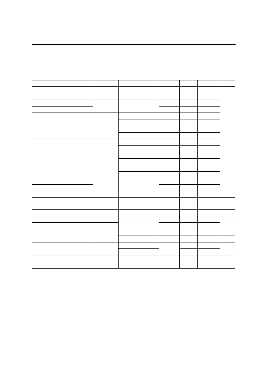
AC Characteristics
(1) External program memory control
(V
DD
= 4.5 to 5.5 V, Ta = �40 to +85�C)
Parameter
Symbol
Condition
Min.
Max.
Unit
Cycle time
t
cyc
f
OSC
= 25 MHz
40
--
Clock pulse width (HIGH level)
t
WH
13
--
Clock pulse width (LOW level)
t
WL
13
--
ALE pulse width
t
AW
2t
� 10
--
PSEN
pulse width
t
PW
2t
� 18
--
PSEN
pulse delay time
t
PAD
t
� 5
--
Low address setup time
t
ALS
2t
� 15
--
Low address hold time
t
ALH
t
� 13
--
High address setup time
t
AHS
3t
� 30
--
High address hold time
t
AHH
�8
--
Instruction setup time
t
IS
30
--
Instruction hold time
t
IH
C
L
= 50 pF
�8
t
� 3
ns
Note: t
= t
cyc
/2
t
cyc
t
WH
t
WL
t
AW
t
PAD
t
PW
t
ALS
t
ALH
CPUCLK
ALE
PSEN
AD0 to AD7
A8 to A16
t
IS
t
AHS
t
IH
t
AHH
Bus timing during no wait cycle time
PC0 to 7
INST0 to 7
PC8 to 16

PEDL66517-03
1Semiconductor
ML66517 Family
20/28
(2) External data memory control
(V
DD
= 4.5 to 5.5 V, Ta = �40 to +85�C)
Parameter
Symbol
Condition
Min.
Max.
Unit
Cycle time
t
cyc
f
OSC
= 25 MHz
40
--
Clock pulse width (HIGH level)
t
WH
13
--
Clock pulse width (LOW level)
t
WL
13
--
ALE pulse width
t
AW
2t
� 10
--
RD
pulse width
t
RW
2t
� 18
--
WR
pulse width
t
WW
2t
� 18
--
RD
pulse delay time
t
RAD
t
� 5
--
WR
pulse delay time
t
WAD
t
� 5
--
Low address setup time
t
ALS
2t
� 15
--
Low address hold time
t
ALH
t
� 13
--
High address setup time
t
AHS
3t
� 30
--
High address hold time
t
AHH
t
� 3
--
Read data setup time
t
RS
30
--
Read data hold time
t
RH
0
t
� 3
Write data setup time
t
WS
2t
� 30
--
Write data hold time
t
WH
C
L
= 50 pF
t
� 3
--
ns
Note: t
= t
cyc
/2
t
cyc
t
WH
t
WL
t
AW
t
RAD
t
RW
t
ALS
t
ALH
CPUCLK
ALE
RD
AD0 to AD7
A8 to A15
t
RS
t
AHS
t
RH
t
AHH
Bus timing during no wait cycle time
t
WAD
t
WW
t
ALS
t
ALH
WR
AD0 to AD7
A8 to A15
t
WS
t
AHS
t
WH
t
AHH
RAP0 to 7
RAP8 to 15
DIN0 to 7
RAP0 to 7
DOUT0 to 7
RAP8 to 15

PEDL66517-03
1Semiconductor
ML66517 Family
21/28
(3) Serial port control
Master mode (Clock synchronous serial port)
(V
DD
= 4.5 to 5.5 V, Ta = �40 to +85�C)
Parameter
Symbol
Condition
Min.
Max.
Unit
Cycle time
t
cyc
fOSC = 25 MHz
40
--
Serial clock cycle time
tSCKC
4 t
cyc
--
Output data setup time
tSTMXS
2t
� 5
--
Output data hold time
tSTMXH
5t
� 10
--
Input data setup time
tSRMXS
13
--
Input data hold time
tSRMXH
CL = 50 pF
0
--
ns
Note: t
= t
cyc
/2
t
cyc
CPUCLK
TXC/RXC
SDOUT
(TXD)
SDIN
(RXD)
t
STMXS
t
STMXH
t
SCKC
t
SRMXS
t
SRMXH

PEDL66517-03
1Semiconductor
ML66517 Family
22/28
Slave mode (Clock synchronous serial port)
(V
DD
= 4.5 to 5.5 V, Ta = �40 to +85�C)
Parameter
Symbol
Condition
Min.
Max.
Unit
Cycle time
t
cyc
fOSC = 25 MHz
40
--
Serial clock cycle time
tSCKC
4 t
cyc
--
Output data setup time
tSTMXS
2t
� 15
--
Output data hold time
tSTMXH
4t
� 10
--
Input data setup time
tSRMXS
13
--
Input data hold time
tSRMXH
CL = 50 pF
3
--
ns
Note: t
= t
cyc
/2
Measurement points for AC timing
TXC/RXC
SDOUT
(TXD)
SDIN
(RXD)
t
STMXS
t
STMXH
t
SCKC
t
SRMXS
t
SRMXH
t
cyc
CPUCLK
V
DD
0 V
0.8 V
0.2 V
0.8 V
0.2 V
PEDL66517-03
1Semiconductor
ML66517 Family
23/28
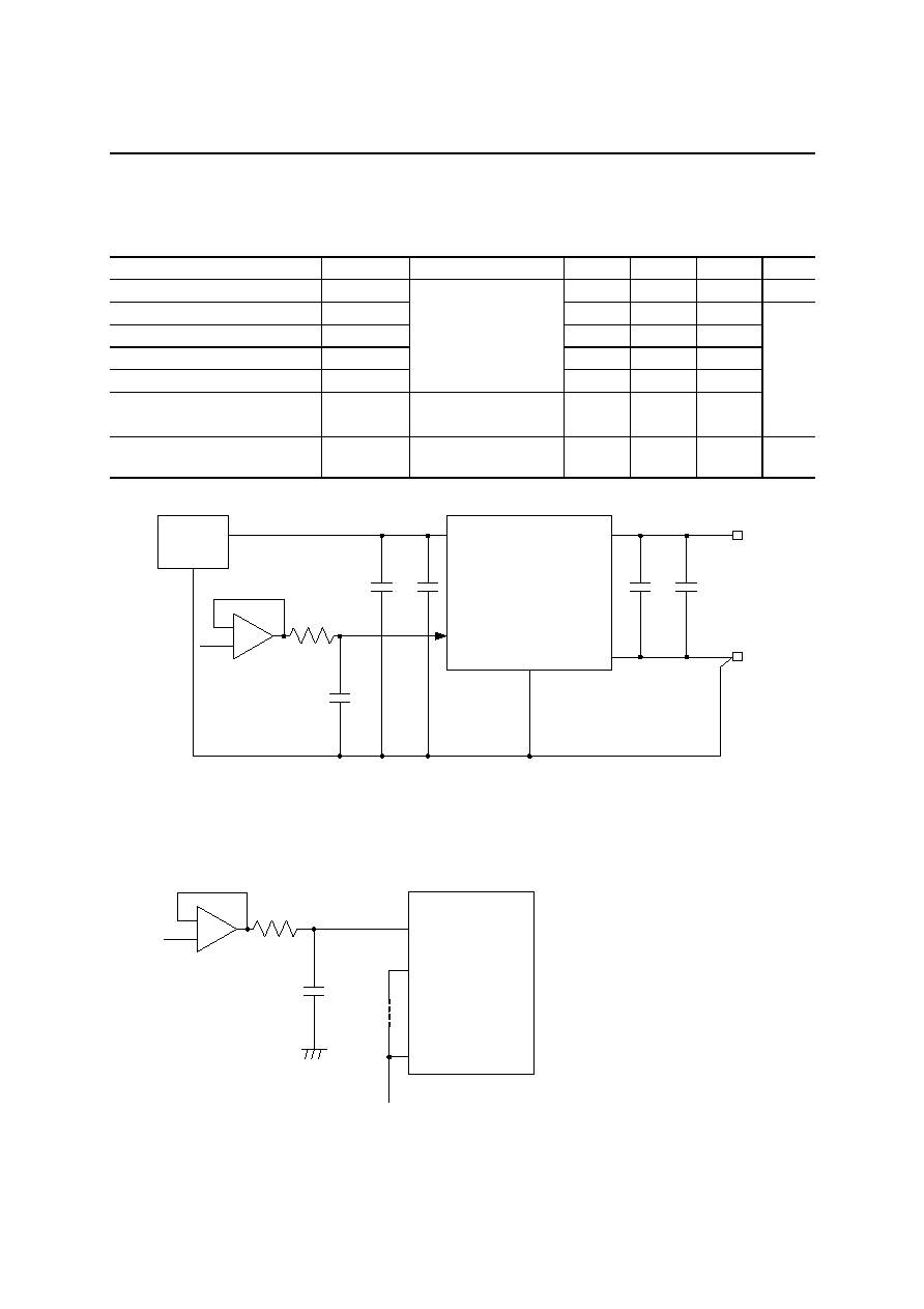
A/D Converter Characteristics
(Ta = �40 to +85�C, V
DD
= 4.5 to 5.5 V, AGND = GND = 0 V)
Parameter
Symbol
Condition
Min.
Typ.
Max.
Unit
Resolution
n
--
10
--
Bit
Linearity error
E
L
--
--
�3
Differential linearity error
E
D
--
--
�2
Zero scale error
E
ZS
--
--
+3
Full-scale error
E
FS
Refer to measurement
circuit 1
Analog input source
impedance RI
5 k
t
CONV
= 10.7 �s
--
--
�3
Cross talk
E
CT
Refer to measurement
circuit 2
--
--
�1
LSB
Conversion time
t
CONV
Set according to
ADTM set data
10.7
--
--
�s/ch
Measurement Circuit 1
Measurement Circuit 2
V
REF
Reference
voltage
V
DD
GND
�
+
Analog input
R
I
AI0 to AI7
C
I
0.1
�
F
47
�
F
+
0.1
�
F
47
�
F
+
+5 V
0 V
AGND
R
I
(impedance of analog input source)
5 k
C
I
0.1
�
F
�
+
Analog input
5 k
0.1
�
F
AI0
AI1
AI7
Cross talk is the difference
between the A/D conversion
results when the same
analog input is applied to AI0
through AI7 and the A/D
conversion results of the
circuit to the left.
to
V
REF
or AGND

PEDL66517-03
1Semiconductor
ML66517 Family
24/28
Definition of Terminology
1. Resolution
Resolution is the value of minimum discernible analog input.
With 10 bits, since 2
10
= 1024, resolution of (V
REF
� AGND)
�
1024 is possible.
2. Linearity error
Linearity error is the difference between ideal conversion characteristics and actual conversion characteristics
of a 10-bit A/D converter (not including quantization error).
Ideal conversion characteristics can be obtained by dividing the voltage between V
REF
and AGND into 1024
equal steps.
3. Differential linearity error
Differential linearity error indicates the smoothness of conversion characteristics. Ideally, the range of analog
input voltage that corresponds to 1 converted bit of digital output is 1LSB = (V
REF
� AGND)
�
1024.
Differential error is the difference between this ideal bit size and bit size of an arbitrary point in the conversion
range.
4. Zero scale error
Zero scale error is the difference between ideal conversion characteristics and actual conversion characteristics
at the point where the digital output changes from 000H to 001H.
5. Full-scale error
Full-scale error is the difference between ideal conversion characteristics and actual conversion characteristics
at the point where the digital output changes from 3FEH to 3FFH.

PEDL66517-03
1Semiconductor
ML66517 Family
25/28
PACKAGE DIMENSIONS
QFP80-P-1420-0.80-BK
Package material
Lead frame material
Pin treatment
Solder plate thicknes
Package weight (g)
Epoxy resin
42 alloy
Solder plating
5 m or more
1.27 TYP.
MIRROR FINISH
(Unit : mm)
Notes for Mounting the Surface Mount Type Packages
The surface mount type packages are very susceptible to heat in reflow mounting and humidity
absorbed in storage.
Therefore, before you perform reflow mounting, contact Oki's responsible sales person for the product
name, package name, pin number, package code and desired mounting conditions (reflow method,
temperature and times).

PEDL66517-03
1Semiconductor
ML66517 Family
26/28
QFP64-P-1414-0.80-BK
Package material
Lead frame material
Pin treatment
Solder plate thickness
Package weight (g)
Epoxy resin
42 alloy
Solder plating
5 m or more
0.87 TYP.
(Unit : mm)
MIRROR FINISH
Notes for Mounting the Surface Mount Type Packages
The surface mount type packages are very susceptible to heat in reflow mounting and humidity
absorbed in storage.
Therefore, before you perform reflow mounting, contact Oki's responsible sales person for the product
name, package name, pin number, package code and desired mounting conditions (reflow method,
temperature and times).

PEDL66517-03
1Semiconductor
ML66517 Family
27/28
SDIP64-P-750-1.778
Package material
Lead frame material
Pin treatment
Solder plate thickness
Package weight (g)
Epoxy resin
Cu alloy
Solder plating
5 m or more
8.70 TYP.
(Unit : mm)

PEDL66517-03
1Semiconductor
ML66517 Family
28/28
NOTICE
1. The information contained herein can change without notice owing to product and/or technical improvements.
Before using the product, please make sure that the information being referred to is up-to-date.
2. The outline of action and examples for application circuits described herein have been chosen as an explanation
for the standard action and performance of the product. When planning to use the product, please ensure that
the external conditions are reflected in the actual circuit, assembly, and program designs.
3. When designing your product, please use our product below the specified maximum ratings and within the
specified operating ranges including, but not limited to, operating voltage, power dissipation, and operating
temperature.
4.
Oki assumes no responsibility or liability whatsoever for any failure or unusual or
unexpected operation resulting from misuse, neglect, improper installation, repair, alteration
or accident, improper handling, or unusual physical or electrical stress including, but not
limited to, exposure to parameters beyond the specified maximum ratings or operation
outside the specified operating range.
5. Neither indemnity against nor license of a third party's industrial and intellectual property right, etc. is granted
by us in connection with the use of the product and/or the information and drawings contained herein. No
responsibility is assumed by us for any infringement of a third party's right which may result from the use
thereof.
6. The products listed in this document are intended for use in general electronics equipment for commercial
applications (e.g., office automation, communication equipment, measurement equipment, consumer
electronics, etc.). These products are not authorized for use in any system or application that requires special or
enhanced quality and reliability characteristics nor in any system or application where the failure of such
system or application may result in the loss or damage of property, or death or injury to humans.
Such applications include, but are not limited to, traffic and automotive equipment, safety devices, aerospace
equipment, nuclear power control, medical equipment, and life-support systems.
7. Certain products in this document may need government approval before they can be exported to particular
countries. The purchaser assumes the responsibility of determining the legality of export of these products and
will take appropriate and necessary steps at their own expense for these.
8. No part of the contents contained herein may be reprinted or reproduced without our prior permission.
Copyright 1999 Oki Electric Industry Co., Ltd.