
FEDL7022-01-06
1Semiconductor
This version: May 2000
Previous version: Sep. 1999
ML7022-01
Single Rail Dual Channel PCM CODEC
1/20
GENERAL DESCRIPTION
The ML7022 is a two-channel single-rail CODEC CMOS IC for voice signals ranging from 300 to 3400Hz. This
device contains two-channel analog-to-digital (A/D) and digital-to-analog (D/A) converters on a single chip. The
ML7022 is designed especially for a single power supply and low power applications and achieves a reduced
footprint.
The ML7022 is best suited for line card applications with easy interface to subscriber line interface circuits
(SLICs). The SLIC interface latches are embedded onto this CODEC, thus eliminating the need for external
components and optimizing board space.
FEATURES
∑
Single 5 V Power Supply Operation
∑
Using
-
ADC and DAC Technique
∑
Low Power Consumption
2-Channel Operating Mode:
typical: 70 mW
max.: 90 mW
1-Channel Operating Mode:
typical: 40 mW
max.: 55 mW
Power Saving Mode: (CPD1 = CPD2 = "0")
typical: 9 mW
max.: 12.5 mW
Power Down Mode: (PDN = "0")
typical: 0.05 mW
max.: 0.25 mW
∑
ITU-T Companding Law -
µ
-law
∑
Built-in Dual 3-bit Latches with CMOS Drive Capability
∑
Serial PCM Interface
∑
Master Clock: 4.096 MHz
∑
Transmission Clocks:
256 to 4096 kbps
∑
Adjustable Transmit Gain
∑
Built-in Reference Voltage Supply
∑
Analog Output can Directly Drive a 600
Line Transformer
∑
Latched Content Echo-back Function
∑
Package Type:
30-pin plastic SSOP (SSOP30-P-56-0.65-K) (Product name: ML7022-01MB)

FEDL7022-01-06
1Semiconductor
ML7022-01
2/20
BLOCK DIAGRAM
RC
LPF
RC
LPF
RC
LPF
RC
LPF
-
AD
CONV
BPF
BPF
LPF
LPF
-
AD
CONV
-
DA
CONV
-
DA
CONV
AIN1
GSX
1
Co
m
p
re
s
s
o
r
Co
m
p
re
s
s
o
r
E
x
pander
E
x
pander
DOUT
TC
O
N
T
AOUT
1
AOUT
2
RCON
T
BCLK
XS
YN
C
RSY
N
C
DIN
AIN2
GSX
2
LAT
C
H
C1A
C2A
C3A
C1B
C2B
C3B
Pow
e
r C
ont.
&
C
l
ock
G
en.
PDN
MCK
SG
G
en.
SGC
V
DD
AG
DG

FEDL7022-01-06
1Semiconductor
ML7022-01
3/20
PIN CONFIGURATION (TOP VIEW)
30-Pin Plastic SSOP
1
V
DD
TEST1
TEST2
AIN1
GSX1
AOUT1
TEST3
AG
SGC
AOUT2
GSX2
AIN2
TEST4
TEST5
V
DD
PDN
C1A
C2A
C3A
RSYNC
XSYNC
DG
DOUT
DIN
BCLK
MCK
C3B
C2B
C1B
TEST6
2
3
4
5
6
7
8
9
10
11
12
13
14
15
30
29
28
27
26
25
24
23
22
21
20
19
18
17
16
FEDL7022-01-06
1Semiconductor
ML7022-01
4/20
PIN DESCRIPTIONS
Pin
Symbol
Type
Description
1
V
DD
--
Power Supply *
2
TEST1
I
Device Test Pin 1
3
TEST2
I
Device Test Pin 2
4
AIN1
I
Channel-1 Transmit Op-amp Input
5
GSX1
O
Channel-1 Transmit Op-amp Output
6
AOUT1
O
Channel-1 Receive Output
7
TEST3
I
Device Test Pin 3
8
AG
--
Analog Ground
9
SGC
O
Signal Ground
10
AOUT2
O
Channel-2 Receive Output
11
GSX2
O
Channel-2 Transmit Op-amp Output
12
AIN2
I
Channel-2 Transmit Op-amp Input
13
TEST4
I
Device Test Pin 4
14
TEST5
I
Device Test Pin 5
15
V
DD
--
Power Supply *
16
TEST6
I
Device Test Pin 6
17
C1B
O
C1B Bit Latched Output
18
C2B
O
C2B Bit Latched Output
19
C3B
O
C3B Bit Latched Output
20
MCK
I
Master Clock (4.096 MHz)
21
BCLK
I
Shift Clock for the DIN and DOUT
22
DIN
I
Data Input
23
DOUT
O
Data Output
24
DG
--
Digital Ground
25
XSYNC
I
Transmit Synchronizing Signal
26
RSYNC
I
Receive Synchronizing Signal
27
C3A
O
C3A Bit Latched Output
28
C2A
O
C2A Bit Latched Output
29
C1A
O
C1A Bit Latched Output
30
PDN
I
Power Down Control
* V
DD
of pin 1 and V
DD
of pin 15 are connected internally, but these pins must be connected on the printed
circuit board.
FEDL7022-01-06
1Semiconductor
ML7022-01
5/20
ABSOLUTE MAXIMUM RATINGS
Parameter
Symbol
Condition
Rating
Unit
Power Supply Voltage
V
DD
--
≠0.3 to +7.0
V
Analog Input Voltage
V
AIN
--
≠0.3 to V
DD
+0.3
V
Digital Input Voltage
V
DIN
--
≠0.3 to V
DD
+0.3
V
Storage Temperature
T
STG
--
≠55 to +150
∞
C
RECOMMENDED OPERATING CONDITIONS
Parameter
Symbol
Condition
Min.
Typ.
Max.
Unit
Power Supply Voltage
V
DD
Voltage must be fixed
4.75
5.0
5.25
V
Operating Temperature
T
OP
--
≠40
--
+85
∞
C
Analog Input Voltage
V
AIN
Gain = 1
--
--
3.4
V
PP
High Level Input Voltage
V
IH
2.2
--
V
DD
V
Low Level Input Voltage
V
IL
All Digital Input Pins
0
--
0.8
V
MCK Frequency
F
MCK
MCK
≠0.01%
4096
+0.01%
kHz
BCLK Frequency
F
BCLK
BCLK
256
--
4096
kHz
Sync Pulse Frequency
F
SYNC
XSYNC, RSYNC
--
8
--
kHz
Clock Duty Ratio
D
CLK
MCK, BCLK
40
50
60
%
Digital Input Rise Time
T
IR
--
--
50
ns
Digital Input Fall Time
T
IF
All Digital Input Pins
--
--
50
ns
MCK to BCLK Phase
Difference
T
MB
MCK, BCLK
--
--
50
ns
T
XS
BCLK to XSYNC
50
--
--
ns
Transmit Sync Pulse Setting
Time
T
SX
XSYNC to BCLK
50
--
--
ns
T
RS
BCLK to RSYNC
50
--
--
ns
Receive Sync Pulse Setting
Time
T
SR
RSYNC to BCLK
50
--
--
ns
Sync Pulse Width
T
WS
XSYNC, RSYNC
1 BCLK
--
100
µ
s
DIN Set-up Time
T
DS
DIN
50
--
--
ns
DIN Hold Time
T
DH
DIN
50
--
--
ns
R
DL
Pull-up Resistor, DOUT
0.5
--
--
k
DOUT
--
--
50
pF
Digital Output Load
C
DL
C1A, C2A, C3A,C1B, C2B, C3B
--
--
50
pF
Bypass Capacitor for SGC
C
SG
SG to AG
0.1
--
--
µ
F

FEDL7022-01-06
1Semiconductor
ML7022-01
6/20
ELECTRICAL CHARACTERISTICS
DC and Digital Interface Characteristics
(V
DD
= 4.75 to 5.25 V, Ta = ≠40 to +85
∞
C)
Parameter
Symbol
Condition
Min.
Typ.
Max.
Unit
I
DD1
2CH Operating Mode, No Signal
PDN = "1", CPD1 = CPD2 = "1"
--
14.0
18.0
mA
I
DD2
1CH Operating Mode, No Signal
PDN = "1", CPD1 = "1", CPD2 =
"0" or PDN = "1", CPD1 = "0",
CPD2 = "1"
--
8.0
11.0
mA
I
DD3
Power Saving Mode,
PDN = "1", CPD1 = CPD2 = "0"
--
1.8
2.5
mA
Power Supply Current
I
DD4
Power Down Mode,
PDN = "0"
--
0.01
0.05
mA
High Level Input Leakage
Current
I
IH
All Digital Input Pins
V
I
= V
DD
--
--
2.0
µ
A
Low Level Input Leakage
Current
I
IL
All Digital Input Pins
V
I
= 0 V
--
--
0.5
µ
A
DOUT, Pull-up = 0.5 k
0
0.2
0.4
V
Digital Output Low Voltage
V
OL
C1A, C2A, C3A, C1B, C2B, C3B
I
OL
= 0.4 mA
0
0.2
0.4
V
C1A, C2A, C3A, C1B, C2B, C3B
I
OH
= 0.4 mA
2.5
--
--
V
Digital Output High Voltage
V
OH
C1A, C2A, C3A, C1B, C2B, C3B
I
OH
= 50
µ
A
V
DD
≠0.5
--
--
V
Digital Output Leakage
Current
I
O
DOUT High Impedance State
--
--
10
µ
A
Input Capacitance
C
IN
--
--
5
--
pF
Analog Interface Characteristics
(V
DD
= 4.75 to 5.25 V, Ta = ≠40 to +85
∞
C)
Parameter
Symbol
Condition
Min.
Typ.
Max.
Unit
SGC Rise Time
T
SGC
SG to AG 0.1
µ
F
Rise time to 90% of max. level
--
--
10
ms
Transmit Analog Interface Characteristics
(V
DD
= 4.75 to 5.25 V, Ta = ≠40 to +85
∞
C)
Parameter
Symbol
Condition
Min.
Typ.
Max.
Unit
Input Resistance
R
INX
AIN1, AIN2
10
--
--
M
Output Load Resistance
R
LGX
20
--
--
k
Output Load Capacitance
C
LGX
--
--
30
pF
Output Amplitude
V
OGX
GSX1, GSX2
with respect to SG
*1
≠1.13
--
1.13
V
Offset Voltage
V
OSGX
Gain = 1
≠20
--
20
mV
*1 0.27 dBm (600
) = 3.17 dBm0 (
µ
-law) = 2.26 V
PP
FEDL7022-01-06
1Semiconductor
ML7022-01
7/20
Receive Analog Interface Characteristics
(V
DD
= 4.75 to 5.25 V, Ta = ≠40 to +85
∞
C)
Parameter
Symbol
Condition
Min.
Typ.
Max.
Unit
Output Load Resistance
R
LAO
AOUT1, AOUT2 (each)
with respect to SG
0.6
--
--
k
Output Load Capacitance
C
LAO
AOUT1, AOUT2
--
--
50
pF
Output Amplitude
V
OAO
AOUT1, AOUT2, R
LAO
= 0.6 k
with respect to SG
≠1.7
--
1.7
V
Offset Voltage
V
OSAO
AOUT1, AOUT2
with respect to SG
≠100
--
100
mV
AC Characteristics
(V
DD
= 4.75 to 5.25 V, Ta = ≠40 to +85
∞
C)
Condition
Parameter
Symbol
Freq.
(Hz)
Level
(dBm0)
Min.
Typ.
Max.
Unit
Loss T1
60
25
45
--
Loss T2
300
≠0.15
0.15
0.20
Loss T3
1020
Reference
Loss T4
3000
≠0.15
0.02
0.20
Loss T5
3300
≠0.15
0.1
0.80
Transmit
Frequency Response
Loss T6
3400
0
GSXn to DOUT
(Attenuation)
0
0.6
0.80
dB
Loss R1
100
≠0.15
0.04
0.2
Loss R2
1020
Reference
Loss R3
3000
≠0.15
0.07
0.2
Loss R4
3300
≠0.15
0.2
0.8
Receive
Frequency Response
Loss R5
3400
0
DIN to AOUTn
(Attenuation)
0
0.6
0.8
dB
SDT1
3
36
43
--
SDT2
0
36
40
--
SDT3
≠30
36
38
--
SDT4
≠40
30
32
--
Transmit
Signal to Distortion
Ratio
SDT5
1020
≠45
GSXn to DOUT
*2
25
29
--
dB
SDR1
3
36
42
--
SDR2
0
36
39
--
SDR3
≠30
36
39
--
SDR4
≠40
30
33
--
Receive
Signal to Distortion
Ratio
SDR5
1020
≠45
DIN to AOUTn
*2
25
30
--
dB
GTT1
3
≠0.2
0.02
0.2
GTT2
≠10
Reference
GTT3
≠40
≠0.2
0.06
0.2
GTT4
≠50
≠0.6
0.4
0.6
Transmit
Gain Tracking
GTT5
1020
≠55
GSXn to DOUT
≠1.2
0.4
1.2
dB
GTR1
3
≠0.2
0
0.2
GTR2
≠10
Reference
GTR3
≠40
≠0.2
≠0.02
0.2
GTR4
≠50
≠0.6
≠0.1
0.6
Receive
Gain Tracking
GTR5
1020
≠55
DIN to AOUTn
≠1.2
≠0.2
1.2
dB
NIDLE
T
--
--
AINn = SG *2
AINn to DOUT
--
14
16
Idle Channel Noise
NIDLE
R
--
--
DIN = 0 code *2
DIN to AOUTn
--
6
10
dBrnc0
*2 C-message Filter is used

FEDL7022-01-06
1Semiconductor
ML7022-01
8/20
AC Characteristics (Continued)
(V
DD
= 4.75 to 5.25 V, Ta = ≠40 to +85
∞
C)
Condition
Parameter
Symbol
Freq.
(Hz)
Level
(dBm0)
Min.
Typ.
Max.
Unit
AV
T
GSXn to DOUT
V
DD
= 5 V,
Ta = 25
∞
C
0.535
0.555
0.574
Absolute Level
(Initial Difference)
AV
R
DIN to AOUTn
V
DD
= 5 V,
Ta = 25
∞
C
0.806
0.835
0.864
Vrms
AV
TT
≠0.3
--
0.3
Absolute level
(Deviation of
Temperature and
power)
AV
RT
1020
0
V
DD
= 4.75 to 5.25 V
Ta = ≠40 to 85
∞
C
≠0.3
--
0.3
dB
Absolute Delay
T
D
1020
0
A to A Mode
BCLK = 2048 kHz
--
0.58
0.6
ms
T
GD
T1
500
--
0.26
0.75
T
GD
T2
600
--
0.16
0.35
T
GD
T3
1000
--
0.02
0.125
T
GD
T4
2600
--
0.05
0.125
Transmit Group Delay
T
GD
T5
2800
0
*3
--
0.07
0.75
ms
T
GD
R1
500
--
0.00
0.75
T
GD
R2
600
--
0.00
0.35
T
GD
R3
1000
--
0.00
0.125
T
GD
R4
2600
--
0.09
0.125
Receive Group Delay
T
GD
R5
2800
0
*3
--
0.12
0.75
ms
CR
T
Trans to Receive
75
83
--
CR
R
Receive to Trans
75
80
--
Cross Talk
Attenuation
CR
CH
1020
0
Channel to Channel
75
78
--
dB
Discrimination
DIS
4.6 to 72k
0
0 to 4 kHz
30
32
--
dB
Out of Band Spurious
OBS
300 to
3.4k
0
4.6 kHz to 1000 kHz
--
≠37.5
≠35
dB
SFD
T
--
≠50
≠40
Signal Frequency
Distortion
SFD
R
1020
0
0 to 4 kHz
--
≠48
≠40
dBm0
IMD
T
--
≠50
≠40
Intermoduration
Distortion
IMD
R
fa = 470
fb = 320
≠4
2 fa - fb
--
≠54
≠40
dBm0
PSR
T1
0 to 4k
40
44
--
PSR
T2
4 to 50k
50
55
--
PSR
R1
0 to 4k
40
45
--
Power Supply Noise
Rejection Ratio
PSR
R2
4 to 50k
100
mVrms
*4
50
56
--
dB
T
SD
20
--
100
T
XD1
20
--
100
T
XD2
DOUT
Pull-up resister = 0.5 k
C
L
= 50 pF and 1 LSTTL
20
--
100
ns
Digital Output
Delay Time
T
PDC
C1A, C2A, C3A, C1B, C2B, C3B
C
L
= 50 pF and 1 LSTTL
20
--
1000
ns
DOUT Operation
Delay Time
T
DDO
Time of operation start after power on
--
4
--
ms
AOUT Signal Output
Delay Time
T
DAO
Time of base band signal output start
after power on
--
4
--
ms
*3 Minimum value of the group delay distortion
*4 The measurement under idle channel noise

FEDL7022-01-06
1Semiconductor
ML7022-01
9/20
TIMING DIAGRAM
Figure 1 Transmit Side Timing Diagram
Figure 2 Receive Side Timing Diagram
Figure 3 Transmit Side Bit Configuration
Figure 4 Receive Side Bit Configuration
MCK
T
XS
D2
1
2
3
4
5
6
7
8
T
SX
T
XD1
T
SD
D3
D4
D5
D6
D7
D8
MSD
T
WS
T
XD2
T
MB
BCLK
XSYNC
DOUT
T
RS
D2
1
2
3
4
5
6
7
8
T
SR
T
DS
T
WS
T
DH
D3
D4
D5
MSD
D6
D7
D8
T
MB
MCK
BCLK
RSYNC
DIN
MS
D
EC
3
A
D2
D3
D4
D5
D6
D7
D8
EPD
1
EC
2
A
EC
1
A
MS
D
EC
3
B
D2
D3
D4
D5
D6
D7
D8
EPD
2
EC
2
B
EC
1
B
MS
D
D2
D3
1
9
17
25
1
CH1 PCM DATA ECHO bits
CH2 PCM DATA ECHO bits
BCLK
XSYNC
DOUT
MS
D
C3A
D2
D3
D4
D5
D6
D7
D8
CP
D1
C2A
C1A
MS
D
C3B
D2
D3
D4
D5
D6
D7
D8
CP
D2
C2B
C1B
MS
D
D2
D3
1
9
17
25
1
CH1 PCM DATA
CH1 power down control bit
CH2 PCM DATA
Latch Data
CH2 power down control bit
Latch Data
BCLK
RSYNC
DIN
FEDL7022-01-06
1Semiconductor
ML7022-01
10/20
MSD
D2
D3
D4
D5
D6
D7
D8
CPD1
C3A
C2A
C1A
MSD
D2
D3
D4
D5
D6
D7
D8
CPD2
C3B
C2B
C1B
MSD
D2
D3
D4
D5
D6
D7
D8
CPD1
C3A
C2A
C1A
MSD
D2
D3
D4
D5
D6
D7
D8
CPD2
C3B
C2B
C1B
CH1
PC
M
I
N
P
U
T D
A
TA
C
ontrol
DAT
A
CH2
PC
M
I
N
P
U
T D
A
TA
C
ontrol
DAT
A
CH1
PC
M
I
N
P
U
T D
A
TA
C
ontrol
DAT
A
CH2
PC
M
I
N
P
U
T D
A
TA
C
ontrol
DAT
A
1
9
17
25
1
9
17
25
MSD
D2
D3
D4
D5
D6
D7
D8
EPD1
EC3A
EC2A
EC1A
MSD
D2
D3
D4
D5
D6
D7
D8
EPD2
EC3B
EC2B
EC1B
MSD
D2
D3
D4
D5
D6
D7
D8
EPD1
EC3A
EC2A
EC1A
MSD
D2
D3
D4
D5
D6
D7
D8
EPD2
EC3B
EC2B
EC1B
CH1
PC
M
OUT
P
UT
DA
T
A
ECHO
BIT
CH2
PC
M
OUT
P
UT
DA
T
A
ECHO
BIT
CH2
PC
M
OUT
P
UT
DA
T
A
ECHO
BIT
CH1
PC
M
OUT
P
UT
DA
T
A
ECHO
BIT
T
PDC
T
PDC
BCLK
XS
YN
C
RSY
N
C
DIN
DOUT
C3
A, C2
A,
C1
A, C3
B,
C2
B, C1
B
Figur
e
5
Contr
o
l Bit T
i
ming a
nd Ec
ho Ba
c
k
T
i
ming
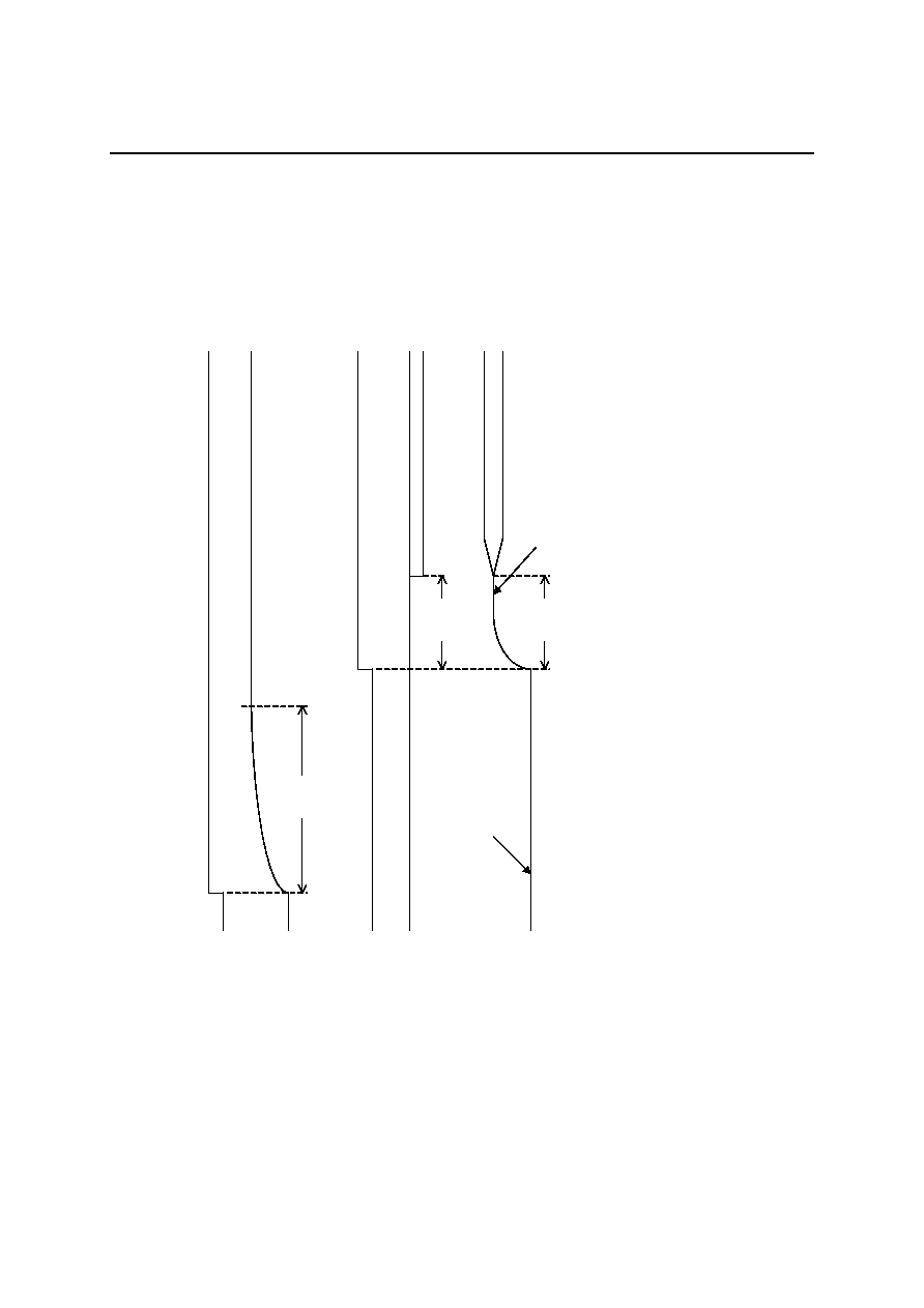
FEDL7022-01-06
1Semiconductor
ML7022-01
11/20
Figur
e
6
S
G
C,
DOUT
a
nd
A
O
UT
Output
T
i
ming
PDN
CPD1
(CPD2)
DOUT
SGC
T
SGC
T
DDO
T
DA
O
A
OUT
n
SG Lev
e
l
H
i
gh I
m
pe
dan
ce

FEDL7022-01-06
1Semiconductor
ML7022-01
12/20
FUNCTIONAL DESCRIPTION
Pin Functional Description
AIN1, AIN2, GSX1, GSX2
AIN1 and AIN2 are the transmit analog inputs for Channels 1 and 2.
GSX1 and GSX2 are the transmit level adjustments for Channels 1 and 2.
AIN1 and AIN2 are inverting inputs for the op-amp; GSX1 and GSX2 are connected to the output of the op-amp
and are used to adjust the level, as shown below.
If AIN1 and AIN2 are not used, connect AIN1 to GSX1 and AIN2 to GSX2. During power saving and power down
mode, the GSX1 and GSX2 outputs are at AG voltage.
In the case of the analog input 2.26 Vpp at GSX pin with digital output +3.17 dBm0 (
µ
-law).
AOUT1, AOUT2
AOUT1 is the receive analog output for Channel 1 and AOUT2 is used for Channel 2.
The output signal has an amplitude of 3.4Vpp above and below the signal ground voltage (SG).When the digital
signal of +3.17 dBm0 is input to DIN, it can drive a load of 600
or more.
During power saving or power down mode, these outputs are at a high impedance.
V
DD
Power supply for +5 V.
Connect a bypass capacitor of 0.1
µ
F with excellent high frequency characteristics between this pin and the AG
pin.
Although V
DD
pin 1 and V
DD
pin 15 are connected internally, these pins must be connected on the printed circuit
board.
CH1 Gain
Gain = R2/R1
10
R1: Variable
R2
>
20 k
C1
>
1/ (2
◊
3.14
◊
30
◊
R1)
CH2 Gain
Gain = R4/R3
10
R3: Variable
R4
>
20 k
C2
>
1/ (2
◊
3.14
◊
30
◊
R3)
CH1
Analog
Input
GSX1
AIN1
SG
R2
R1
C1
CH2
Analog
Input
GSX2
AIN2
SG
R4
R3
C2

FEDL7022-01-06
1Semiconductor
ML7022-01
13/20
AG
Ground for the analog signal circuits.
DG
Ground for the digital signal circuits.
This ground is separate from the analog signal ground. The DG pin must be connected to the AG pin on the printed
circuit board to make a common analog ground.
SGC
Used to generate the signal ground voltage level, by connecting a bypass capacitor. Connect a 0.1
µ
F capacitor
with excellent high frequency characteristics between the AG pin and the SGC pin.
During power down mode, this outputs are at the voltage level of AG with about 50 k
impedance.
MCK
Master clock input.
The frequency must be 4.096 MHz.
BCLK
Shift clock signal input for the DIN and DOUT signals.
The frequency, equal to the data rate, is 256 k to 4096 kHz. This signal must be synchronized in phase with the
MCK (generated from the same clock source as MCK). Figure 1 shows the phase difference of MCK and BCLK.
RSYNC
Receive synchronizing signal input.
Signals in the receive section are synchronized by this synchronizing signal. This signal must be synchronized in
phase with the MCK (generated from the same clock source as MCK).
XSYNC
Transmit synchronizing signal input.
The PCM output signal from the DOUT pin is output in synchronization with this transmit synchronizing signal.
This synchronizing signal synchronizes all timing signals of all section. This signal must be synchronized in phase
with the MCK (generated from the same clock source as MCK).

FEDL7022-01-06
1Semiconductor
ML7022-01
14/20
DIN
DIN is a data input pin.
The voice band signal is converted to an analog signal in synchronization with the RSYNC signal and BCLK. The
analog signal of channel 1 is output from AOUT1 pin and the analog signal of channel 2 is output from AOUT2
pin.
The 28 bit signal structure is shown in Figure 4. It consists of voice band PCM signals (8 bits each), the general-
purpose latch signal (6 bits total), the power down control signal (1 bit per channel) and empty bits (4 bits). The
signal is shifted at a falling edge of the BCLK signal and latched into the internal register when shifted by 28 bits.
The start of the PCM data (Channel 1's MSD) is identified at the rising edge of RSYNC.
The general purpose latch signal (C3A, C2A, C1A, C3B, C2B, C1B) are output from six latch output pins.
When the CPD1 (bit of DIN) = "0", Channel 1 block is in a power down state. When the CPD2 (bit of DIN) = "0",
Channel 2 block is in a power down state.
DOUT
DOUT is a data output pin.
The signal consist of a total of 28 bits containing the voice band PCM signals (each channel 8 bits), the echo bit (6
bits for latch signal and 2 bits for power down state indication), and empty bits (4 bits). The output cording format
follows ITU-T recommendation on coding law.
The output signal is output from Channel 1's MSD bit in a sequential order, synchronizing with the rising edge of
the BCLK signal. The first bit of DOUT may be output at the rising edge of the XSYNC signal, based on the timing
between BCLK and XSYNC.
This pin is in a high impedance state during power down state.
A pull-up resistor must be connected to this pin because it is an open drain output.
Table 1 The Output Cording Format
PCMIN/PCMOUT
µ
-law
INPUT/OUTPUT
Level
MSD
D2
D3
D4
D5
D6
D7
D8
+ Full scale
1
0
0
0
0
0
0
0
+0
1
1
1
1
1
1
1
1
≠0
0
1
1
1
1
1
1
1
≠ Full scale
0
0
0
0
0
0
0
0

FEDL7022-01-06
1Semiconductor
ML7022-01
15/20
C1A, C2A, C3A, C1B, C2B, C3B
General-purpose latched output signal.
C1A, C2A, C3A, C1B, C2B, C3B bits of DIN are latched using internal timing.
These outputs can drive a LSTTL/CMOS device without external resistor.
PDN
Power down control signal.
When PDN is at logic "0" level, both Channel 1 and Channel 2 circuits are in the power down state. Also, all
internal latches are in initial state (logic "0" level).
TEST1, TEST2, TEST3, TEST4, TEST5, TEST6
These pins are used for device test.
These device test pin must be connected to the AG pin.

FEDL7022-01-06
1Semiconductor
ML7022-01
16/20
Table 2 Condition of DOUT by the Power Control
PDN
CPD1 CPD2
CH1 PCM Data
CH2 PCM Data
CH1 Echo Bit
CH2 Echo Bit
0
0/1
0/1
H
H
H
H
1
0
0
11111111
11111111
1
1
0
Operate
11111111
1
0
1
11111111
Operate
1
1
1
Operate
Operate
Latched Data
Latched Data
Table 3 Condition of the Latched Output by the Power Control
PDN
CPD1 CPD2
LIN
C1A, C2A, C3A
C1B, C2B, C3B
0
0/1
0/1
L
L
1
0/1
0/1
0
Latched Data
Latched Data
0/1
0/1
0/1
1
L
L
Table 4 Condition of the Analog Output by the Power Control
PDN
CPD1 CPD2
GSX1
GSX2
AOUT1
AOUT2
SGC
0
0/1
0/1
High
Impedance
High
Impedance
High
Impedance
High
Impedance
*5
1
0
0
High
Impedance
High
Impedance
High
Impedance
High
Impedance
Operate
1
1
0
Operate
High
Impedance
Operate
High
Impedance
Operate
1
0
1
High
Impedance
Operate
High
Impedance
Operate
Operate
1
1
1
Operate
Operate
Operate
Operate
Operate
*5 The voltage level of AG with about 50 k

FEDL7022-01-06
1Semiconductor
ML7022-01
17/20
APPLICATION CIRCUITS
M
L7022
A
IN1
GSX
1
A
OUT
1
A
IN2
GSX
2
A
OUT
2
SGC
A
G
DG
V
DD
DOUT
DIN
MCK
BCLK
XS
YN
C
RSY
N
C
PDN
TE
S
T
1
TE
S
T
2
TE
S
T
3
TE
S
T
4
TE
S
T
5
TE
S
T
6
C1
A
C2
A
C3
A
C1
B
C2
B
C3
B
2C
H
M
u
ltiplex
PC
M
signal o
u
tpu
t
2C
H
M
u
ltiplex
PC
M
signal i
npu
t
M
a
ster
clo
ck &
B
i
t c
l
o
ck
inpu
t
M
a
ster
clo
ck &
B
i
t c
l
o
ck
inpu
t
P
o
we
r
d
o
wn
c
o
n
t
r
o
l
0: pow
e
r dow
n
/1: o
p
era
t
ion
Latc
h out
put
C
hanne
l 1
anal
og i
nput
C
hanne
l 1
anal
og o
u
tput
C
hanne
l 2
anal
og i
nput
C
hanne
l 2
anal
og o
u
tput
0 V
+5 V
1 k
+5 V
0.1
µ
F
0.1
µ
F
1
µ
F +

FEDL7022-01-06
1Semiconductor
ML7022-01
18/20
RECOMMENDATIONS FOR ACTUAL DESIGN
∑
To assure specified electrical characteristics, use bypass capacitors with excellent high frequency characteristics
for the power supply and keep them as close as possible to the device pins.
∑
Connect the AG pin and DG pin each other as closely as possible. Connect to the system ground with low
impedance.
∑
Unless unavoidable, use short lead type socket.
∑
When mounted on a frame, use electromagnetic shielding, if any electromagnetic emission sources such as
power supply transformers surround the device.
∑
Keep the voltage on the V
DD
pin not lower than ≠0.3 V even instantaneously to avoid latch-up phenomenon when
turning the power on.
∑
Use a low noise power supply (having low level high frequency spike noise or pulse noise) to avoid erroneous
operation and the degradation of the characteristics of these device.
FEDL7022-01-06
1Semiconductor
ML7022-01
19/20
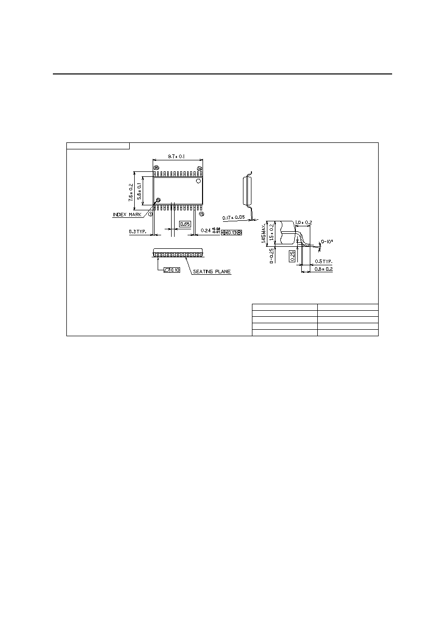
PACKAGE DIMENSIONS
Notes for Mounting the Surface Mount Type Package
The surface mount type packages are very susceptible to heat in reflow mounting and humidity
absorbed in storage.
Therefore, before you perform reflow mounting, contact Oki's responsible sales person for the product
name, package name, pin number, package code and desired mounting conditions (reflow method,
temperature and times).
SSOP30-P-56-0.65-K
Mirror finish
Package material
Epoxy resin
Lead frame material
42 alloy
Pin treatment
Solder plating (
5µm)
Package weight (g)
0.19 TYP.
5
Rev. No./Last Revised
5/Dec. 5, 1996
(Unit: mm)

FEDL7022-01-06
1Semiconductor
ML7022-01
20/20
NOTICE
1.
The information contained herein can change without notice owing to product and/or technical improvements.
Before using the product, please make sure that the information being referred to is up-to-date.
2.
The outline of action and examples for application circuits described herein have been chosen as an
explanation for the standard action and performance of the product. When planning to use the product, please
ensure that the external conditions are reflected in the actual circuit, assembly, and program designs.
3.
When designing your product, please use our product below the specified maximum ratings and within the
specified operating ranges including, but not limited to, operating voltage, power dissipation, and operating
temperature.
4.
Oki assumes no responsibility or liability whatsoever for any failure or unusual or unexpected operation
resulting from misuse, neglect, improper installation, repair, alteration or accident, improper handling, or
unusual physical or electrical stress including, but not limited to, exposure to parameters beyond the specified
maximum ratings or operation outside the specified operating range.
5.
Neither indemnity against nor license of a third party's industrial and intellectual property right, etc. is
granted by us in connection with the use of the product and/or the information and drawings contained herein.
No responsibility is assumed by us for any infringement of a third party's right which may result from the use
thereof.
6.
The products listed in this document are intended for use in general electronics equipment for commercial
applications (e.g., office automation, communication equipment, measurement equipment, consumer
electronics, etc.). These products are not authorized for use in any system or application that requires special
or enhanced quality and reliability characteristics nor in any system or application where the failure of such
system or application may result in the loss or damage of property, or death or injury to humans.
Such applications include, but are not limited to, traffic and automotive equipment, safety devices, aerospace
equipment, nuclear power control, medical equipment, and life-support systems.
7.
Certain products in this document may need government approval before they can be exported to particular
countries. The purchaser assumes the responsibility of determining the legality of export of these products
and will take appropriate and necessary steps at their own expense for these.
8.
No part of the contents contained herein may be reprinted or reproduced without our prior permission.
Copyright 2000 Oki Electric Industry Co., Ltd.