PEDL7048-01-01
1Semiconductor
This version: Oct. 2001
ML7048-01
Preliminary
3-Channel Single Rail CODEC
1/20
GENERAL DESCRIPTION
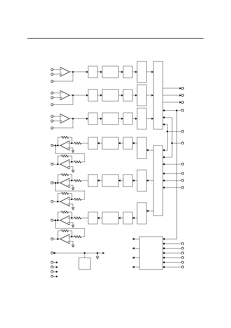
The ML7048 is a three-channel single rail CMOS CODEC LSI. This device contains filters for A-to-D and D-to-
A conversions of voice signals ranging 300 to 3400 Hz.
The ML7048 is designed for a single power supply and low power applications and contains three-channel A-to-
D and D-to-A converters on a single chip, and achieves a reduced footprint and external component parts.
The ML7048 is best suited for ISDN terminal and digital telephone terminal applications.
FEATURES
∑ Single 5 V Power Supply Operation
∑ Using
-
ADC and DAC Technique
∑ Low Power Consumption
3-Channel Operating Mode:
typical: 140 mW
max.:174 mW
Power Saving Mode: (PDN = "1", PDN1 to 3 = "0") typical:
15 mW
max.: 26 mW
Power Down Mode: (PDN = "0")
typical: 0.05 mW
max.: 0.3 mW
∑ ITU-T Companding Law:
µ
-law
∑ PCM Interface:
3-Channel Independent or 3-Channel Continuous Serial Interface Pin Selectable
∑ Master Clock:
12.288 MHz or 15.360 MHz Pin Selectable
∑ Transmission Clocks:
64, 128, 256, 512, 1024, 2048 kHz
96, 192, 384, 768, 1536 kHz
∑ Adjustable Transmit Gain for Each Channel
∑ Built-in Reference Voltage Supply
∑ Differential Analog Output can Directly Drive a 600
Transformer.
∑ Package:
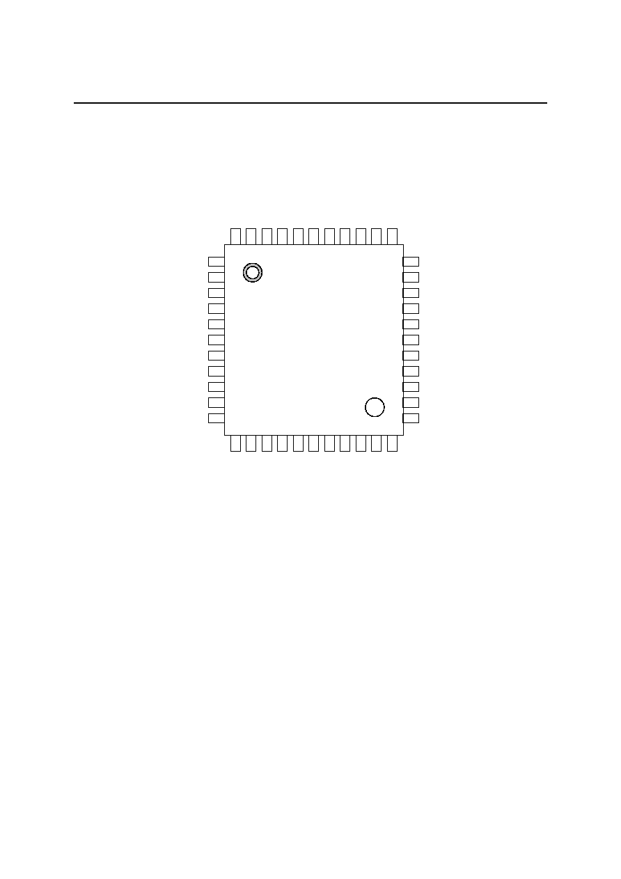
44-pin Plastic QFP (QFP44-P-910-0.80-2K) (Product name: ML7048-01GA)

PEDL7048-01-01
1Semiconductor
ML7048-01
4/20
PIN DESCRIPTION
Pin
Symbol
Type
Description
1
AIN1+
I
Channel-1 Transmit Amp Non-inverting Input
2
VDDA
--
Analog Power Supply
3
AOUT2≠
O
Channel-2 Receive Amp Inverting Output
4
AOUT2+
O
Channel-2 Receive Amp Non-inverting Output
5
GSX2
O
Channel-2 Transmit Amp Output
6
AIN2≠
I
Channel-2 Transmit Amp Inverting Input
7
AG
--
Analog Ground
8
AIN2+
I
Channel-2 Transmit Amp Non-inverting Input
9
VDDA
--
Analog Power Supply
10
SGC
O
Analog Signal Ground
11
AIN3+
I
Channel-3 Transmit Amp Non-inverting Input
12
AIN3≠
I
Channel-3 Transmit Amp Inverting Input
13
GSX3
O
Channel-3 Transmit Amp Output
14
AOUT3+
O
Channel-3 Receive Amp Non-inverting Output
15
AOUT3≠
O
Channel-3 Receive Amp Inverting Output
16
AG
--
Analog Ground
17
DG
--
Digital Ground
18
V
DD
--
Digital Power Supply
19
MCKSEL
I
Master Clock Frequency Select Signal
20
MCK
I
Master Clock
21
BCLK
I
PCM Signal Shift Clock
22
P/S
I
3-Channel Independent/3-Channel Continuous Serial Interface
Select Signal
23
TEST2
I
Test Control Signal 2
24
XSYNC
I
Transmit Sync Signal
25
RSYNC
I
Receive Sync Signal
26
DIN1
I
Channel-1 PCM Signal Input
27
DIN2
I
Channel-2 PCM Signal Input
28
DIN3
I
Channel-3 PCM Signal Input
29
DG
--
Digital Ground
30
DOUT1
O
Channel-1 PCM Signal Output
31
DOUT2
O
Channel-2 PCM Signal Output
32
DOUT3
O
Channel-3 PCM Signal Output
33
TEST3
I
Test Control Signal 3
34
PDN
I
Power Down Control Signal
35
PDN1
I
Channel-1 Power Down Control Signal
36
PDN2
I
Channel-2 Power Down Control Signal
37
PDN3
I
Channel-3 Power Down Control Signal
38
V
DD
--
Digital Power Supply
39
DG
--
Digital Ground
40
AG
--
Analog Ground
41
AOUT1≠
O
Channel-1 Receive Amp Inverting Output
42
AOUT1+
O
Channel-1 Receive Amp Non-inverting Output
43
GSX1
O
Channel-1 Transmit Amp Output
44
AIN1≠
I
Channel-1 Transmit Amp Inverting Input
PEDL7048-01-01
1Semiconductor
ML7048-01
5/20
PIN FUNCTIONAL DESCRIPTION
AIN1+, AIN2+, AIN3+, AIN1≠, AIN2≠, AIN3≠, QSX1, GSX2, GSX3
AIN1+, AIN1≠ and GSX1 are the transmit inputs and transmit level adjustment pins for Channel 1, AIN2+, AIN2≠
and GSX2 are those for Channel 2. AIN3+, and AIN3≠ and GSX3 are those for Channel 3.
AIN1+, AIN2+ and AIN3+ are non-inverting inputs for the op-amp.
AIN1≠, AIN2≠ and AIN3≠ are inverting inputs for the op-amp.
GSX1, GX2 and GX3 are the outputs for op-amp.
Do the level adjustment as described below.
If AINn≠ and AINn+ are not used, connect AINn≠ to GSXn and AINn+ to SGC.
During power saving and power down modes, GSX1, GSX2, and GSX3 outputs are at a high impedance. During
power down mode in each channel, the GSX output of a channel in power down mode is at a high impedance.
AOUT1+, AOUT1≠, AOUT2+, AOUT2≠, AOUT3+, AOUT3≠
AOUT1+ and AOUT1≠ are the receive analog output pins for Channel 1, AOUT2+ and AOUT2≠ are those for
Channel 2, and AOUT3+ and AOUT3≠ are those for Channel 3.
AOUT1≠ is the inverting output for AOUT1+, AOUT2≠ is for AOUT2+, and AOUT3≠ is for AOUT3+. A load of
600
or more can be driven between AOUT1+ and AOUT1≠, AOUT2+ and AOUT2≠, and AOUT3+ and
AOUT3≠. The output signal has an amplitude of 3.4 Vpp above and below the signal ground voltage (SG) when
the digital signal of 3.17 dBm0 is input to DIN1, DIN2, and DIN3.
During power saving and power down modes, the AOUT1+, AOUT1≠, AOUT2+, AOUT2≠, AOUT3+, and
AOUT3≠ outputs are at a high impedance.
During power down mode in each channel, the AOUTn+ and AOUTn≠ of a channel in power down are at a high
impedance.
SGC
Bypass capacitor pin used to generate the signal ground voltage level.
Connect a 1
µ
F capacitor with excellent high frequency characteristics between the SGC pin and the AG pin.
MCK
Master clock input pin. The frequency is 12.288 MHz or 15.360 MHz.
The frequency is switched by MCKSEL. This master clock may be asynchronous with BCLK, RSYNC, and
XSYNC.
MCKSEL
Master clock frequency select signal input pin. Input a 12.288 MHz clock to the MCK pin when MCKSEL is "0".
Input a 15.360 MHz clock to the MCK pin when MCKSEL is "1".
PDN
Power down control signal input pin. When PDN is "0", all circuits are in power down mode.
Channel n gain
Gain = R2n/R1n
10
R1: Variable
R2
>
20 k
C1n
>
1/(2
◊
3.14
◊
30
◊
R1n)
R1 + R2 < 500 k
Channel n
analog input
GSXn
AINn≠
SGC
R2n
R1n
C1n
AINn+
SG
Gen.