OKI Semiconductor
FEDL7055-02
Issue Date: Apr. 8, 2003
ML7055
Bluetooth Baseband Controller IC
1/30
GENERAL DESCRIPTION
The ML7055 is a CMOS digital IC for use in 2.4 GHz band BluetoothTM systems. This IC incorporates the
ARM7TDMI
as the CPU core, features a highly expandable architecture, and supports the interfaces for a variety
of applications. Since the ML7055 has Oki's Bluetooth protocol stack software installed, when the IC is used in
conjunction with the Bluetooth RF transceiver IC, data/voice communications are possible while maintaining
interconnectivity with other Bluetooth systems.
FEATURES
� Conforms to Bluetooth Specification (Ver1.1)
� Designed for connection with the RF-LSI interface, such as the OKI RF-LSI interface (ML7050), the
SKYWORKS RF-LSI interface (CX72303), or the BROADCOM RF-LSI interface (BCM2002X) that
functions as the Bluetooth RF-LSI interface
� The high-speed, low-power ARM7TDMI
TM
is installed as the CPU core
� PCM-CVSD transcoder that provides high quality voice using the noise filter is installed
� Low power consumption in flexible power management modes according to operating modes of Bluetooth
�
DETACH signal provides control of change to power-saving mode (STOP) and return request to normal
mode.
� UART interface corresponding to baud rates up to 921.6 kbps
� I
2
C bus interface provides accesses to EEPROM or PCM-Codec
� Selactable 12 MHz or 13 MHz for the system clock
� Selectable 32 kHz or 32.768 kHz for the LPO clock
� Built-in programmed ROM eliminates external ROM/FLASH
� The packages are available in three types:
63-pin WCSP for ML7055HB
64-pin BGA for ML7055LA
84-pin BGA for ML7055LP
ARM, ARM7TDMI and Thumb are registered trademarks of ARM Ltd., UK.
BLUETOOTH is a trademark owned by Bluetooth SIG, Inc. and licensed to Oki Electric Industry.
The information contained herein can change without notice owing to the product being under development.
FEDL7055-02
OKI Semiconductor
ML7055
2/30
SPECIFICATIONS
Process 0.16
�
m CMOS (5-layer metal wire)
Package
63-pin WCSP (P-VFLGA63-4.90
�
4.72-0.50-W)
(Dimensions: 4.90 mm
�
4.72 mm
�
0.48 mm; pin pitch: 0.50 mm)
64-pin BGA (P-TFBGA64-0707-0.65)
(Dimensions: 7 mm
�
7 mm
�
1.2 mm; pin pitch: 0.65 mm)
84-pin BGA (P-LFBGA84-0909-0.80)
(Dimensions: 9 mm
�
9 mm
�
1.5 mm; pin pitch: 0.80 mm)
Supply current
22 mA (24 MHz operation)
Operating voltage ranges
2.70 to 3.6 V for input-output, 1.65 to 1.95 V for internal circuits
Operating frequency
24 MHz
Built-in ROM size
176 KB (for ARM program)
Built-in RAM size
24 KB
Input clocks
12 MHz or 13 MHz (system clock)
32 kHz or 32.768 kHz (LPO clock)
RF-LSI interface
OKI RF-LSI interface (ML7050)
SKYWORKS RF-LSI interface (CX72303
)
BROADCOM RF-LSI interface (BCM2002X)
Installed interfaces
UART interface (up to 921.6 Kbps)
General-purpose I/O interface (used as a pin for I
2
C bus interface
depending on software installed)
PCM interface (PCM Linear/A-law/
�
-law can be selected)
DETACH interface
Timers
16-bit auto reload timer (1ch)
18-bit auto reload timer (1ch)
Interrupt controller
11 causes
Clock control circuit
Crystal oscillator circuit (12 MHz or 13 MHz, 32 kHz or 32.768 kHz)
Internal PLL

FEDL7055-02
OKI Semiconductor
ML7055
3/30
PIN PLACEMENT
ML7055HB: 63-pin WCSP (P-VFLGA63-4.90
� 4.72-0.50-W)
LVDD
VDD GND
SOUT
GND
PLL
_PS
PLL_
DATA
Core
VDD
SFRQ
SEL
VDD
GND
TX_POW
TXD
RSSI_
CLK
1
2
3
4
5
6
7
8
A
B
C
D
E
F
G
H
PLL
_POW
RSSI
PLL
LOCK
VDD
XC32KN
SCLK
SEL
XC32KP
GND
AVDD1
AVDD0
SCLKN
AGND1
GND
Core
VDD
SCLKP
DETACH
GND
RTS
Core
VDD
GND
RFSEL2
GND GND
VDD
Core
VDD
GND
GND
RX_
POW
PLL
_OFF
PLL
_CLK
GND
PCM
OUT
Core
VDD
RXD
PLL_LE
PCM
SYNC
PCM
CLK
GND
SIN RFSEL1
SDA
SCL PCMIN
RESET
AGND0 RFSEL0 CTS CLKOUT VDD
TOP VIEW
FEDL7055-02
OKI Semiconductor
ML7055
4/30
ML055LA: 64-pin BGA (P-TFBGA64-0707-0.65)
TOP VIEW
Core
VDD
XC32KN
RSSI
PLL
LOCK
VDD
1
2
3
4
5
6
7
8
A
B
C
D
E
F
G
H
J
K
XC32KP
GND AGND1
AVDD0
AGND0
GND
Core
VDD
SCLKP
SCLKN
VDD
DETACH
RFSEL0
9
10
RTS
Core
VDD RFSEL2
AVDD1
SCLK
SEL
GND
RFSEL1
RESET
SFRQ
SEL
RXD
TXD
GND
PLL_
CLK
PLL_PS PLL_LE
RX_
POW
PLL_
POW
TX_
POW
PLL_
OFF
PLL_
DATA
RSSI_
CLK
LVDD GND
GND
VDD
SOUT
GND
SIN
GND
Core
VDD
GND
VDD
CTS
CLKOUT GND
SDA SCL
Core
VDD
VDD
PCM
SYNC
PCMIN GND
PCM
CLK
PCMOUT
GND
Core
VDD
GND
FEDL7055-02
OKI Semiconductor
ML7055
5/30
ML7055LP: 84-pin BGA (P-LFBGA84-0909-0.80)
TOP VIEW
Core
VDD
VDD
RXD
NC
XC32KN
1
2
3
4
5
6
7
8
A
B
C
D
E
F
G
H
J
K
XC32KP
GND AVDD1
AGND1
AGND1
AGND0
AVDD0
GND
AGND0
VDD
GND
NC
9
10
CTS
Core
VDD RFSEL2
AVDD1
SFRQ
SEL
RESET
RFSEL0
SCLKN
SCLK
SEL
PLL
LOCK
GND
TXD
PLL_LE PLL_PS
TX_
POW
PLL_
POW
RX_
POW
PLL_
OFF
LVDD
RSSI_
CLK
PLL_
DATA
PLL_
CLK
GND
NC
SOUT
NC
SIN
Core
VDD
NC
GND
GND
VDD
RTS
GND CLKOUT
NC SDA
VDD
NC
PCM
OUT
GND
Core
VDD
PCM
SYNC
GND
GND
Core
VDD
GND
NC
AVDD0
Core
VDD SCLKP
DETACH
RFSEL1
NC
SCL
NC
NC
RSSI
PCMIN
NC
PCMCLK
NC
NC
GND
VDD
GND
NC

FEDL7055-02
OKI Semiconductor
ML7055
6/30
PIN DESCRIPTIONS
RF I/F
Pin Placement
Pin Name
Direc-
tion
[*0]
Internal
Pull Up/
Down,
Schmitt
Initial
Value ML7055
HB
ML7055
LA
ML7055
LP
Description
TXD O --
L
L
L
B6
B4
A4
ML7050: Transmit data output
CX72303: Transmit data output
BCM2002X: Transmit data output
RXD I --
--
--
--
C5
B5
A5
ML7050: Receive data input
CX72303: Receive data input
BCM2002X: Receive data input
PLL_DATA O
--
X
H
L
C7
C2
C1
ML7050: Serial write data
CX72303: Serial write data
BCM2002X: Transmit enable
PLL_CLK O --
L
L
L
E6
D1
D2
ML7050: Serial clock
CX72303: Serial clock
BCM2002X: Serial clock
PLL_LE O --
L
H
L
D5
B3
A3
ML7050: Serial road enable
0: Negate, 1: Assert
CX72303: Serial enable
0: Assert, 1: Negate
BCM2002X: RF-LSI synthesizer on
0: Negate, 1: Assert
RSSI I Pull
down
--
--
--
B5
A5
C5
ML7050: Receive field strength data
input
CX72303: Serial read data
BCM2002X: Serial read data
RSSI_CLK O
--
L
L
X
B8
C1
C2
ML7050: Receive field strength data
clock
CX72303: RF-LSI receiving
characteristic control
BCM2002X: System clock request
H
L
PLL_POW O
--
H
B7
A1
A1
ML7050: Local PLL power control
0: Assert, 1: Negate
CX72303: PA Power control
0: Negate, 1: Assert
BCM2002X: Select serial transmit
mode
H
L
TX_POW O --
L
A8
B2
A2
ML7050: Transmit enable
0: Assert, 1: Negate
CX72303: Transmit enable
0: Negate, 1: Assert
BCM2002X: Serial write data
H
L
RX_POW O --
L
C6 A2 B2
ML7050: Receive enable
0: Assert, 1: Negate
CX72303: Receive enable
0: Negate, 1: Assert
BCM2002X: Receive enable
PLL_PS O --
L
X
L
A7 A3 B3
ML7050: "L"
CX72303: Power on reset
0: Assert (reset) 1: Negate
BCM2002X: RF-LSI receiving
characteristic control
[*0] "I" = Input, "O" = Output, "I/O" = Input/Output
FEDL7055-02
OKI Semiconductor
ML7055
7/30
RF I/F
Pin Placement
Pin Name
Direc-
tion
[*0]
Internal
Pull Up/
Down,
Schmitt
Initial
Value ML7055
HB
ML7055
LA
ML7055
LP
Description
PLLLOCK I
Pull
down
--
--
--
B4 B6 B5
ML7050: --
CX72303: --
BCM2002X: 1MHz clock
H
--
PLL_OFF
O --
L
D6 B1 B1
ML7050: PLL loop control
0: Open loop 1: Closed loop
CX72303: Diversity output
BCM2002X: PA Power control
PCM I/F
Pin Placement
Pin Name
Direc-
tion
Internal
Pull Up/
Down,
Schmitt
Initial
Value ML7055
HB
ML7055
LA
ML7055
LP
Description
PCMOUT
O
--
L
G6
J3
J4
PCM data output
PCMIN
I
Pull up
--
H4
J5
H5
PCM data input
PCMSYNC I/O
Pull
down
-- F5 J4 K4
PCM sync signal (8 kHz),
Initial setting: input
(can be switched by an internal
register)
PCMCLK I/O
Pull
down
-- G5 K4 H4
PCM clock (64 kHz/128 kHz)
Initial setting: input
(can be switched by an internal
register)
Note: The PCM sync signal (8 kHz) must be guaranteed at the accuracy of
�
50 ppm if the
PCMSYNC pin is configured as an input.
UART I/F
Pin Placement
Pin Name
Direc-
tion
Internal
Pull Up/
Down,
Schmitt
Initial
Value ML7055
HB
ML7055
LA
ML7055
LP
Description
SOUT
O
--
H
E7
F1
F2
ACE transmit serial data
SIN
I
Schmitt
--
D4
G1
G2
ACE receive serial data
RTS
O
--
--
G2
J9
K9
ACE transmit data ready
CTS I -- H
F3 K9 J9
ACE transmit ready
FEDL7055-02
OKI Semiconductor
ML7055
8/30
CLK and Configuration
Pin Placement
Pin Name
Direc-
tion
Internal
Pull Up/
Down,
Schmitt
Initial
Value ML7055
HB
ML7055
LA
ML7055
LP
Description
SCLKP
I -- --
E1 E9 F8
SCLKN O -- -- D1 E10 F10
System clock (12/13 MHz) pins
(Power level: CMOS level)
XC32KP I -- -- A2 A9 A9
XC32KN O -- -- A3 A8 B8
Subclock pins (for oscillator)
SCLKSEL I
Pull
down
-- B3 A7 B7
System clock frequency select pin
L: Select CLK divided by
internal PLL
H: Select subclock
SFRQSEL I
Pull
down
-- C4 B7 A7
System clock frequency select pin
L: 13
MHz
H: 12
MHz
RFSEL0�
2
I -- --
[*1] [*2] [*3]
RF-LSI select pins
RFSEL[2:0]
001: ML7050
(OKI)
010: CX72303
(SKYWORKS)
101: BCM2002X
(BROADCOM)
Others: Unused
RESET
I
Schmitt
--
C3
F10
G10
Hardware reset pin (Reset = L)
DETACH
I Schmitt
-- F2 G9 G8
Sleep pin (Sleep = L)
SCL O -- L G4 K7 H7
I
2
C serial clock
SDA I/O -- H F4 J7 K7
I
2
C serial data
CLKOUT O -- -- G3
J8
K8
System clock (12/13 MHz) output
pins
[*1] RFSEL0: E3; RFSEL1: E4; RFSEL2: H1
[*2] RFSEL0: H9; RFSEL1: H10; RFSEL2: K10
[*3] RFSEL0: H10; RFSEL1: H8; RFSEL2: K10
FEDL7055-02
OKI Semiconductor
ML7055
9/30
NC
Pin Placement
Pin Name
Direc-
tion
Internal
Pull Up/
Down,
Schmitt
Initial
Value ML7055
HB
ML7055
LA
ML7055
LP
Description
NC
-- --
[*4]
No
connection
[*4] B6, C3, C4, C6, C7, C8, D3, E1, F1, H2, H3, H6, H9, J6, J7
Note: Do not wire under the NC pin.
Power, GND
Pin Placement
Pin Name
Direc-
tion
Internal
Pull Up/
Down,
Schmitt
Initial
Value ML7055
HB
ML7055
LA
ML7055
LP
Description
V
DD
--
--
--
[*5]
[*6]
[*7]
I/O power supply pin
2.70 to 3.6 V
CoreV
DD
-- -- -- [*8] [*9] [*10]
Power supply pin for internal circuit
1.65 to 1.95 V
LV
DD
-- -- -- C8 D2 D1
RF-I/O power suply pin (Same
voltage to the V
DD
for RF-LSI)
GND
--
--
--
[*11]
[*12]
[*13]
Digital block ground pin
AV
DD
0 -- -- -- B1 C9 [*14]
AV
DD
1 -- -- -- B2 B9 [*15]
Analog block power supply pin
1.65 to 1.95 V
AGND0 -- -- -- D3 C10 [*16]
AGND1 -- -- -- C2 B10 [*17]
Analog block ground pin
[*5] V
DD
: A4, E2, E8, H3, H8
[*6] V
DD
: B8, F2, K1, J6, F9
[*7] V
DD
: A8, F3, K1, K6, F9
[*8] Core
V
DD
: A5, D2, F7, G1, H6
[*9] Core
V
DD
: A6, H1, K3, K6, J10, D10
[*10] Core
V
DD
: A6, G1, K3, K5, J10, E8
[*11] GND: A1, A6, C1, D7, D8, F1, F6, F8, G7, G8, H2, H5, H7
[*12] GND: A4, A10, D9, E1, E2, G2, G10, H2, J1, J2, K2, K5, K8
[*13] GND: A10, B4, E2, E3, E9, G3, G9, H1, J1, J2, J3, J5, J8, K2
[*14] AV
DD
0: D8, D10
[*15] AV
DD
1: B9, B10
[*16] AGND0: E10, D9
[*17] AGND1: C9, C10
FEDL7055-02
OKI Semiconductor
ML7055
10/30
BLOCK DIAGRAM
Default
Slave
T
i
mer
(1ch)
DET
A
CH
IF
176kB
ROM
Default
Slave
ARM7
TD
M
I
AMBA AHB
AMBA APB
TI
C
Arbiter
AHB Ctl
Sy
stem
Control
24kB
RAM
AMBA APB
CT
L/
WDT
I/F
GPIO
I/F
IRC
APB Ctl
Ti
m
e
r
GPIO I/F
CLK
GEN
Clock
ML7055
UART
I/F
UART I/F
IROMC
IRAMC
Processor Bus
APB Ctl
I/F
PCM/
CVSD
I/F
I/F
BT
-BB
Core
I/F
I/F
DETACH
I/F
PCM Codec
RFLSI
SCL
SDA
FEDL7055-02
OKI Semiconductor
ML7055
11/30
DESCRIPTION OF INTERNAL BLOCKS
CLKGEN Block
� Generates a clock that is supplied to each block through SCLKP (12/13 MHz)
� STOP/HALT
function
CTL/WDT Block
� Control of the frequency division function of the internal main clock
� Control of clock supplied to each peripheral
� Control of reset of each peripheral
� STOP/HALT
control
� Watchdog timer function (interrupt/reset)
Timer Block
� 1
channel
� 18-bit timer counter
� Interrupt by compare function
� One shot, interval, or free-run mode
Base band Core Block
� RF
Controller
- RF power supply control (PLL, TX, RX)
- Local PLL frequency division ratio setting
- Receive clock regeneration function
- Synchronization detection (synchronizing within the permissable error limit of SyncWord)
-
Receive
clock
re-timing function
� FH Controller hopping
-
Sequence
control
- Frequency hopping selection function
- CRC computation's initial value selection function
Packet
Decomposer
FHCNT
RF
CNT
Packet
Composer
RF LSI
Tx SCO Buffer
Timing
Codec
I/F
ARM
I/F
RXD
TXD
Audio
APB
Tx ACL Buffer
Rx SCO Buffer
Rx ACL Buffer
Security
CNT

FEDL7055-02
OKI Semiconductor
ML7055
12/30
� Timing
Generator
- Bluetooth clock generation
- Operation interrupts depend on mode (slot, scan, sniff, hold, park)
- Sync detection timing generation (sync window �10
�s)
- PLL setting timing generation
- Transmit/Receive timing generation
- Multi-master timing management function
� Packet
Composer
- Access code generation (SyncWord generation, appending PR*TRAILER)
- Packet header generation (HEC generation, scrambling, FEC encoding)
- Payload generation (CRC generation, encryption, scrambling, FEC encoding)
-
Packet
synthesis
� Packet
Decomposer
- Packet decomposition (separating the packet header and the payload)
- Packet header processing (FEC decoding, descrambling, HEC error detection, header information
separation)
- Payload processing (FEC decoding, descrambling, encryption decoding, CRC judgement, payload
separation)
� Security
- Various key generation functions (initialization, link key, encryption key)
-
Certification
function
-
Encryption
function
FEDL7055-02
OKI Semiconductor
ML7055
13/30
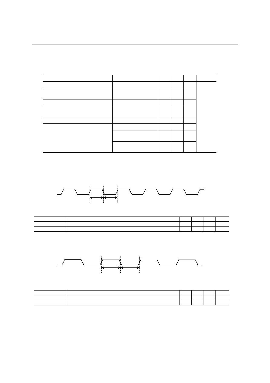
UART Block
� Full-duplex buffering method
� All status reporting function
� Built-in 64-byte transmit/receive FIFO
� Modem control based on CTS
� Programmable serial interface
� 5-, 6-, 7-, 8-bit characters
� Generation and verification of odd parity, even parity, or no parity
� 1, 1.5, or 2 stop bits
� Programmable Baud Rate Generator (9600 bps to 921.6 kbps)
� Error servicing for parity, overrun, and framing errors
� Configuration of 1 Data Frame during Reception
� Configuration of 1 Data Frame during Transmission
SIN
SAMPLE CLK
5 data bits to
8 data bits
Parity
Stop
Start
SOUT
Start
5 data bits to
8 data bits
Parity
Stop

FEDL7055-02
OKI Semiconductor
ML7055
14/30
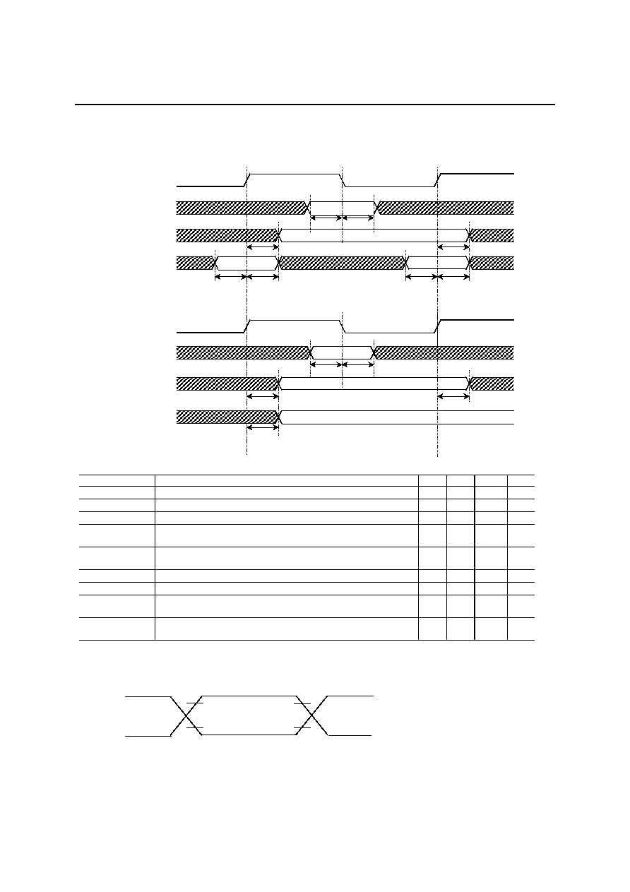
PCM-CVSD Transcoder Block
� Application side I/O:
-
PCM
Codec
� Application-side
format:
- PCM linear (8, 14, 16 bits/sample, 8 kHz sampling frequency)/A-law/
�-law
� Bluetooth-side
format:
-
CVSD/A-law/
�-law
� All combinations of the above conversions are supported
� PCMSYNC/PCMCLK I/O can be switched (initial setting: input)
� Timing in Short Mode and in PCMCLK and PCMSYNC Output Mode
(For PCM data of 14 bits/sample, lower 2 bits of 16 bits are invalid.)
� Timing in Short Mode and in PCMCLK and PCMSYNC Input Mode.
(For PCM data of 14 bits/sample, lower 2 bits of 16 bits are invalid.)
125
�
s (8kHz)
PCMCLK(I)
64k/128kHz
PCMSYNC(I)
8 bits or 16 bits
PCMCLK(O)
64k/128kHz
PCMSYNC(O)
LSB
MSB
DATA
DATA
DATA
LSB
DATA
MSB
Data is output on the rising edge of CLK.
PCMOUT
LSB
MSB
DATA
DATA
DATA
LSB
DATA
MSB
PCMIN
Data is shifted in on the falling edge of CLK
125
�
s (8kHz)
8 bits or 16 bits
LSB
MSB
DATA
DATA
DATA
LSB
DATA
MSB
Data is output on the rising edge of CLK.
PCMOUT
LSB
MSB
DATA
DATA
DATA
LSB
DATA
MSB
PCMIN
Data is shifted in on the falling edge of CLK
FEDL7055-02
OKI Semiconductor
ML7055
15/30
� Timing in Long Mode and in PCMCLK and PCMSYNC Output mode
(For PCM data of 14 bits/sample, lower 2 bits of 16 bits are invalid.)
� Timing in Long Mode and in PCMCLK and PCMSYNC Input Mode.
(For PCM data of 14 bits/sample, lower 2 bits of 16 bits are invalid.)
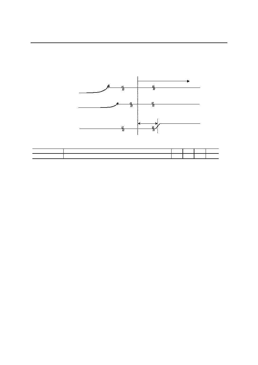
DETACH Interface Block
� Generation of the request for change to (from) the stop mode by detection of the rising (falling) edge of
the
DETACH signal
MSB
DATA
DATA
DATA
DATA
LSB
DATA
MSB
8 bits or 16 bits
Data is output on the rising edge of CLK.
PCMCLK(I)
64k/128kHz
PCMOUT
MSB
DATA
DATA
DATA
DATA
LSB
DATA
MSB
PCMIN
Data is shifted in on the falling edge of CLK.
PCMCLK period (Min.) or
62.5
�
s (Max.)
125
�
s (8kHz)
MSB
DATA
DATA
DATA
DATA
LSB
DATA
MSB
8 bits or 16 bits
Data is output on the rising edge of CLK
PCMCLK(O)
64k/128kHz
PCMSYNC(O)
PCMOUT
MSB
DATA
DATA
DATA
DATA
LSB
DATA
MSB
PCMIN
Data is shifted in on the falling edge of CLK
PCMCLK period
�
3
125
�
s (8kHz)
FEDL7055-02
OKI Semiconductor
ML7055
16/30
ABSOLUTE MAXIMUM RATINGS
Parameter Symbol
Conditions
Rating
Unit
I/O power supply voltage
V
DD
/LV
DD
--
�0.3 to +4.5
V
Core power supply voltage
CoreV
DD
/AV
DD
--
�0.3 to +2.5
V
Input voltage
V
I
--
�0.3 to +4.5
V
Allowable power dissipation
P
d
-- 0.62 W
Storage temperature
T
stg
--
�55 to 150
�C
RECOMMENDED OPERATING CONDITIONS
Parameter Symbol
Conditions
Min.
Typ.
Max.
Unit
I/O power supply voltage
V
DD
/LV
DD
--
2.7 3.3 3.6
V
Core power supply voltage
CoreV
DD
/AV
DD
-- 1.65
1.8
1.95
V
"H" level input voltage
Vih
--
2.2
--
V
DD
V
"L" level input voltage
Vil
--
0
--
0.8
V
Operating temperature
Ta
--
�40
--
85
�C
ELECTRICAL CHARACTERISTICS
DC Characteristics
(V
DD
= 2.7 to 3.6 V, CoreV
DD
= 1.65 to 1.95 V, Ta = �40 to +85�C)
Parameter Symbol
Conditions Min.
Typ.
Max.
Unit
3.0V
Vdd
3.6V 2.4 -- --
"H" level output voltage
Voh
Ioh =
�2 mA
2.7V
Vdd
<
3.0V 2.2 -- --
V
"L" level output voltage
Vol
Iol = 2 mA
--
--
0.4
V
Vi = GND to 3.6 V
�10
--
10
Vi = V
DD
50 k
Pull-down
10 66 200
Input leakage current
Ii
Vi = GND
50 k
Pull-up
�200 �66 �10
�
A
Vo = GND to V
DD
�10
--
10
Output leakage current
Io
Vo = V
DD
50 k
Pull-down
10 66 200
�
A
Power supply current (during
operation)
Iddo
During 24 MHz operation
0 22 32
mA
Power supply current (during
stand-by)
Idds CLK
stopped --
10
100
�
A
FEDL7055-02
OKI Semiconductor
ML7055
17/30
Power Supply Current (IDDO) Characteristics by Power Saving Mode
(V
DD
= 2.7 V to 3.6V, CoreV
DD
= 1.65 V to 1.95V, Ta = -40 to 85�C)
Operating mode
Conditions
Min. Typ. Max. Unit
STOP mode (
DETACH
=
"L")
--
-- 0.03 --
Page Scan operating mode
Interval:1.28sec
Window:11.25msec
-- 2.5 --
Poll Interval operating mod
Interval:40slot
-- 3.5 --
Sniff operating mode
Interval:2000slot
Attempt:4frame
-- 2.5 --
Hold operating mode
Interval:4000slot
-- 0.05 --
DH1/DM1
-- 22.0 --
RX:DH3/DM3
TX:DH1/DM1
-- 22.0 --
ACL operating mode
RX:DH5/DM5
TX:DH1/DM1
-- 22.0 --
mA
AC Characteristics
System clock (SCLKP)
(V
DD
= 2.7 to 3.6V, CoreV
DD
= 1.65 to 1.95V, Ta = -40 to 85�C)
Parameter Description
Min
Typ
Max
Unit
Tmc0
Duty in SCLKP "H" duration
40
50
60
%
Tmc1
Duty in SCLKP "L" duration
40
50
60
%
Sub-clock (XC32KP)
(V
DD
= 2.7 to 3.6V, CoreV
DD
= 1.65 to 1.95V, Ta = -40 to 85�C)
Parameter Description
Min
Typ
Max
Unit
Tmp0
Duty in XC32KP "H" duration
40
50
60
%
Tmp1
Duty in XC32KP "L" duration
40
50
60
%
SCLKP
Tmc0 Tmc1
XC32KP
Tmp0 Tmp1
FEDL7055-02
OKI Semiconductor
ML7055
18/30
Reset
(V
DD
= 2.7 to 3.6V, CoreV
DD
= 1.65 to 1.95V, Ta = -40 to 85�C)
Parameter Description
Min
Typ
Max
Unit
T
RESW
Reset pulse width
10
--
--
�
s
Note : Apply "L" to the
RESET pin for 10 �sec or more after the power supply has been settled.
V
dd
/LV
dd
RESET
Power supply stable period
T
RESW
CoreV
dd
/AV
dd
FEDL7055-02
OKI Semiconductor
ML7055
19/30
PCM interface
(Vdd = 2.7 to 3.6V, CoreVdd = 1.65 to 1.95V, Ta = -40 to 85�C)
Parameter Description
Min
Typ
Max
Unit
Tpc0
PCMIN setup time relative to PCMCLK (input) falling edge
100
--
--
ns
Tpc1
PCMIN hold time relative to PCMCLK (input) falling edge
100
-- --
ns
Tpc2
PCMOUT delay time relative to PCMCLK (input) rising edge
--
--
250 ns
Tpc3
PCMSYNC (input) setup time relative to PCMCLK (input)
rising edge
100
-- --
ns
Tpc4
PCMSYNC (input) hold time relative to PCMCLK (input)
rising edge
100
-- --
ns
Tpc5
PCMIN setup time relative to PCMCLK (output) falling edge
100
-- --
ns
Tpc6
PCMIN hold time relative to PCMCLK (output) falling edge
100
-- --
ns
Tpc7
PCMOUT delay time relative to PCMCLK (output) rising
edge
--
--
250 ns
Tpc8
Delay time from PCMCLK (output) rising edge to PCMSYNC
(output)
--
--
150 ns
AC Characteristic Measuring Points
V
DD
0 V
0.8V
DD
0.2V
DD
0.8V
DD
0.2V
DD
PCMCLK(I)
PCMIN
PCMOUT
Tpc2
Tpc2
Tpc0 Tpc1
PCMSYNC(I)
Tpc3 Tpc4
Tpc3 Tpc4
PCMCLK(O)
PCMIN
PCMOUT
Tpc5
Tpc6
PCMSYNC(O)
Tpc 8
Tpc7
Tpc 7

FEDL7055-02
OKI Semiconductor
ML7055
20/30
REFERENCE FOR VOLTAGE SUPPLY CIRCUIT
� Insert appropriate bypass capacitors between the V
DD
and GND lines.
Note 1: Precautions to insert the bypass capacitors
- Use traces of V
DD
and GND lines wider than those of the other signal lines.
- Keep the length of traces between the bypass capacitors and the V
DD
line and between the bypass
capacitors and the GND line as short as possible.
- Keep the length of traces between the bypass capacitors and the V
DD
line and between the bypass
capacitors and the GND line as equal as possible.
The circuit is subject to change according to the specific LSI board design. Please contact Oki Electric Industry Co.,
Ltd. for detailed information.
Feed lines should be separated
from LSI pins.
Example of ML7055 voltage supply circuit
Capacitors should locate close to LSI pins.
GND
VDD
CoreVDD
ML7055
AVDD0
AGND0
AVDD1
AGND1
0.1
�
F
10 to 47
�
F 0.1
�
F 0.1
�
F
CoreVDD
0.1
�
F
0.1
�
F 0.1
�
F
VDD
GND
10 to 47
�
F
10 to 47
�
F 0.1
�
F 0.1
�
F
LVDD

FEDL7055-02
OKI Semiconductor
ML7055
21/30
REFERENCE FOR OSCILLATOR CIUCUIT
Note 1: The values of C0 and C1, and R0 and R1 should be determined according to the specifications for the
external crystal X'tal 1 (32 or 32.768 kHz).
The values of C2 and C3, and R2 and R3 should be determined according to the specifications for the
external crystal X'tal 2 (13 or 12 MHz).
Note 2: The crystal oscillator circuit should be connected to pins SCLKP and SCLKN only when the OKI RF-LSI
(ML7050) is connected. In other cases, the system clock should be input from the RF-LSI to pin SCLKP.
Note 3: In the case of 13 MHz or 12 MHz system clock (SCLKP) input, make sure the crystal frequency tolerance
is �20 ppm for temperature, supply voltage, and aging.
In the case of 32 kHz or 32.768 kHz sub-clock (XC32KP) input, make sure the crystal frequency tolerance
is �250 ppm for temperature, supply voltage, and aging.
Note 4: Precautions to build a crystal oscillator circuit
- Keep length of wire traces as short as possible.
- Do not cross the crystal oscillator circuit wires over other signal line wires.
- Do not keep signal line wires through which high current flows close to the crystal oscillator circuit.
- Keep the grounding point of the capacitors in the oscillator circuit at the potential equal to GND. And do
not connect the capacitors to the GND or GND lines through which high current flows.
- Do not output signals from the oscillator circuit.
The circuit is subject to change according to the specific LSI board design. Please contact Oki Electric Industry Co.,
Ltd. for detailed information. It is recommended to determine the final circuit values including the capacitance of
the circuit board designed by the user.
ML7055
XC32KP
XC32KN
C1
C0
R0
X'tal 1
R1
SCLKP
SCLKN
C3
C2
R2
X'tal 2
R3
Example of oscillator circuit
Connect this oscillator circuit only when
connecting the OKI RF-LSI ML7050.

FEDL7055-02
OKI Semiconductor
ML7055
22/30
APPLICATION NOTES
Clock Selection
� The system clock frequency is selected according to external pin SFRQSEL.
SFRQSEL = 0 : A 13 MHz clock is input to external pins SCLKP.
SFRQSEL = 1 : A 12 MHz clock is input to external pins SCLKP.
� The CPU clock supply source is selected according to external pin SCLKSEL.
SCLKSEL = 0 : Use the clock that was divided down from the internal PLL output of 192 MHz that
was generated from external pins SCLKP. (Dividing ratios are selectable in the
range of 1/6 to 1/16. Initial value is 1/8 (24 MHz).)
SCLKSEL = 1 : Use external pins XC32KP.
Note: The clock supply source can be set by the CLKCNTL register in the CTL/WDT block once the
LSI is powered up.
� The frequency of CPU clock is selectable from the high speed (24 MHz) and low speed (16 MHz). This
can be performed by the Vendor Specific Command.
Setting the Reset
� Apply a "L" level to the
RESET pin for more than 10 �s after power voltage is stabilized. When the
system clock oscillator circuit is stable and the
RESET pin is at a "H" level, the internal reset is released
and operation starts after the internal reset is held for 1.9 ms for the input clock of 13 MHz or 2.0 ms for
the input clock of 12 MHz.
Setting the UART Baud Rate
� It is possible to set the UART baud rate using the Vendor Specific Commands.
Available baud rate settings:
9600/19.2k/38.4k/56k/57.6k/115.2k/230.4k/345.6k/460.8k/921.6k
(Initial value is 115.2 kbps.)
Setting the PCM-CVSD Transcoder
� It is possible to set the PCM-CVSD transcoders using the Vendor Specific Commands.
For command details, contact Oki Electric Industry Co., Ltd.
� It is possible to set the following parameters using the VCCTL command:
-
PCMSYNC/PCMCLK
mode
(initial setting: input)
- Mute reception (initial setting: OFF)
- Mute transmission (initial setting: OFF)
-
Air
coding
CVSD (initial setting)/
�-law/A-law
-
Interface
coding
Linear (initial setting)/
�-law/A-law
- PCM format (data width of one PCM Linear sample)
8-bit (initial setting)/14-bit/16-bit
- Serial interface format
Short frame (initial setting)/long frame

FEDL7055-02
OKI Semiconductor
ML7055
23/30
- Application interface mode
PCM Codec I/F (initial setting)/APB I/F
XTAL Input Frequency of BCM2002X
� If the system clock is supplied from BCM2002X, the XTAL input frequency of BCM2002X must be 13
MHz. 12, 19.2, 19.68, or 19.8 MHz should not be applied.
XTAL Input Frequency of CX72303
� If the system clock is supplied from CX72303, the XTAL input frequency of CX72303 must be 13 MHz.
10 MHz should not be applied.
Required processes when interface pins are unused
� The following tables show the processes that should be performed when interface pins are not used.
� The pins that are not included in the following table should be left open.
RF I/F
Pin Name
Process When Pin Not Used
Comments
RXD GND
RSSI
Open or GND
PLLLOCK
Open or GND
UART I/F
Pin Name
Process When Pin Not Used
Comments
SIN V
DD
CTS GND
PCM I/F
Pin Name
Process When Pin Not Used
Comments
PCMIN
Open or V
DD
PCMSYNC
Open or GND
PCMCLK
Open or GND
Processes of Other Pins
TEST I/F etc.
Pin Name
Process When Pin Not Used
Comments
DETACH
Pull up or V
DD
FEDL7055-02
OKI Sem
i
conduct
o
r
ML
7055
24/
30
68k
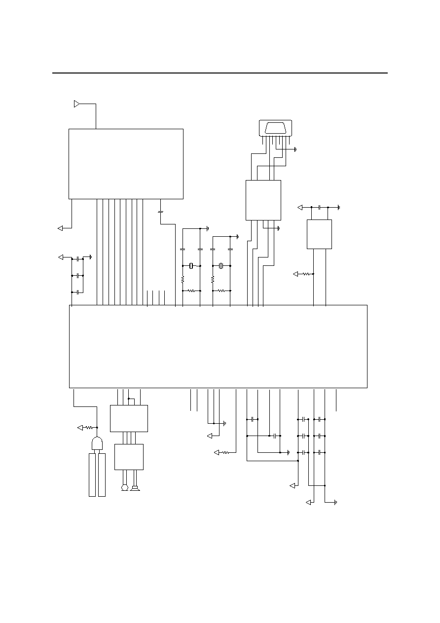
VDD
VDD
MSM7702-01
PCMOUT
PCMIN
RSYNC
BCLK
XSYNC
VDD_D
RXD
PLL_LE
PLL_DATA
PLL_CLK
PLL_OFF
TXD
PLL_POW
RX_POW
TX_POW
MCLK
ANT
RESET
PCMOUT
PCMIN
PCMSYNC
PCMCLK
SCLKSEL
SFRQSEL
RFSEL2
RFSEL1
RFSEL0
DETACH
AVDD0
AGND0
AVDD1
AGND1
CoreVDD
VDD
GND
NC
LVDD
RXD
PLL_LE
PLL_DATA
PLL_CLK
PLL_OFF
TXD
PLL_POW
RX_POW
TX_POW
RSSI
RSSI_CLK
PLL_PS
PLLLOCK
CLKOUT
SCLKN
SCLKP
XC32KN
XC32KP
SOUT
RTS
SIN
CTS
SDA
SCL
RFVDD
VDD
CoreVDD
GND
GND
GND
GND
GND
DSUB9PIN
UART
I/F
4
5
6
7
8
9
1
2
3
TD
RD
RTS
CTS
GND
SDA
SCL
Vcc
GND
VDD
AT24C02
GND
T1IN
T2IN
T3IN
R1OUT
R2OUT
T1OUT
T2OUT
R1IN
R2IN
GND
VDD
MAX3245
32kHz or
47k
VDD
68k
ML7050
ML7055
VDD
GND
The capacitors should be
as close to the LSI pins
as possible.
Separate, as far as
possible, the wiring
from the board pins.
Microphone
Speaker
Voice input/
output
peripherals
Poewr on reset
Hardware reset
ML7055/ML7050
System Configuration Example
0.1
�
0.1
�
47
�
13MHz � 20ppm
32.768kHz � 250ppm
0.1
�
0.1
�
0.1
�
0.1
�
47
�
0.1
�
0.1
�
47
�
FEDL7055-02
OKI Semiconductor
ML7055
25/30
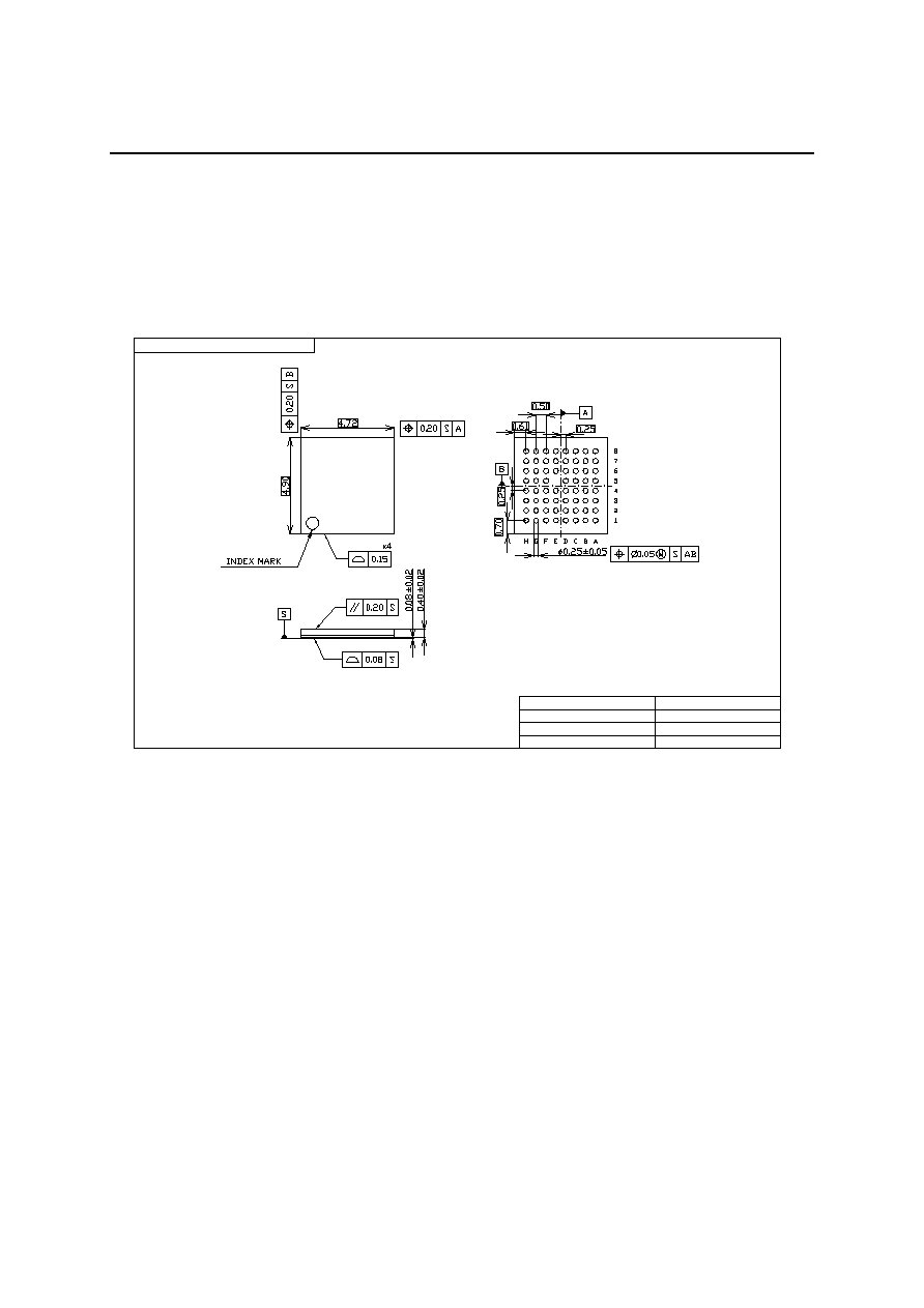
PACKAGE DIMENSIONS
ML7055HB - 63pinWCSP (P-VFLGA63-4.90
� 4.72-0.50-W)
Note: A lead-free package is available. Please contact Oki Sales Office/Distributors for more
information.
P-VFLGA63-4.90
�4.72-0.50-W
Package material
Epoxy resin
Terminal material
Sn/Pb
Package weight (g)
0.03 TYP.
5
Rev. No./Last Revised
1/May 27, 2002
(Unit: mm)
FEDL7055-02
OKI Semiconductor
ML7055
26/30
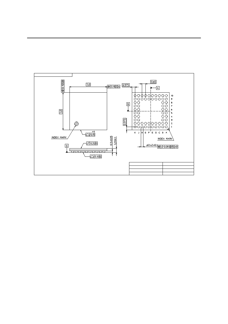
ML7055LA - 64pinBGA (P-TFBGA64-0707-0.65)
P-TFBGA64-0707-0.65
Package material
Epoxy resin
Ball material
Sn/Pb
Package weight (g)
0.10 TYP.
5
Rev. No./Last Revised
1/July 5, 2002
Note: A lead-free package is available. Please contact Oki Sales Office/Distributors for more
information.
(Unit: mm)

FEDL7055-02
OKI Semiconductor
ML7055
27/30
P-LFBGA84-0909-0.80
Package material
Epoxy resin
Ball material
Sn/Pb
Package weight (g)
0.20 TYP.
5
Rev. No./Last Revised
1/May 15, 2000
(Unit: mm)
ML7055LP - 84pinBGA (P-LFBGA84-0909-0.80)
Note: A lead-free package is available. Please contact Oki Sales Office/Distributors for more
information.
Notes for Mounting the Surface Mount Type Package
The surface mount type packages are very susceptible to heat in reflow mounting and humidity
absorbed in storage.
Therefore, before you perform reflow mounting, contact Oki's responsible sales person for the product
name, package name, pin number, package code and desired mounting conditions (reflow method,
temperature and times).
FEDL7055-02
OKI Semiconductor
ML7055
28/30
REVISION HISTORY
Page
Document
No.
Date
Previous
Edition
Current
Edition
Description
PEDL7055-01 Aug.23,
2002
�- �-
Preliminary edition 1
1 1
The contents of the "FEATURES" Section have
been fully changed.
�-
2
Added the "SPECIFICATIONS" Section.
The contents of the table in the "ABSOLUTE
MAXIMUM RATINGS" Section have been
partially changed.
2 3
The voltage values of "Core VDD" have been
added on the table in the "DC Characteristics"
Section.
3 4
The pin name has been changed from LPO_CLK
to TCK.
Eliminated the "LPO_CLK" row in the table of the
"RF/IF" Section.
5 6
Eliminated "Note" on the bottom side of the table
of the "RF/IF" Section.
6 7
The "Description" column of Pin name "TCK" in
the table of the "JTAG I/F" Section has been
partially changed.
8 9
Added "REFERENCE FOR OSCILLATOR
CIRCUIT" Section.
11 13
"DETACH signal" has been changed to
"
DETECH
signal" in the content of the "DETACH
Interface Block" Section.
12 14
Eliminated the "RESET signal input" Section and
added the "Setting the Reset" Section.
�- 15
The "XTAL Input Frequency of BCM2002X" and
"XTAL Input Frequency of CX72303" Sections
have been added.
13 15
Eliminated the "LPO_CLK" row of the "Pin name"
column in the table of the "RF/IF" Section..
PEDL7055-02
Nov. 25, 2002
14-16
16-18
Changed the System Configuration Examples.
1 1
Partially changed the contents of "FEATURES"
Section.
2 2
Changed the contents of "Package" row in the
table.
13 13
Partially added the contents of "UART Block"
Section.
FEDL7055-01
Dec. 17, 2002
13 14
Partially added the contents of "PCM-CVSD"
Section.
FEDL7055-02
OKI Semiconductor
ML7055
29/30
Page
Document
No.
Date
Previous
Edition
Current
Edition
Description
13 15
Partially eliminated the contents of "DETACH
Interface Block" Section.
�- 17-19
Added "Power Supply Current Characteristics by
Power Saving Mode" and "AC Characteristics"
Sections.
9 19
Partially added the contents of "REFERENCE
FOR VOLTAGE SUPPLY CIRCUIT" Section.
10 20
Partially added the contents of "REFERENCE
FOR OSCILLATOR CIRCUIT" Section.
14 22
Partially added the contents of "Clock Selection"
Section.
FEDL7055-01
Dec. 17, 2002
16 24
Partially changed the contents of "System
Configuration Example" Section.
6
6
Partially added the contents of "RF I/F" Section.
16 16
Partially added the contents of "DC
Characteristics" Section.
18 18
Partially eliminated the contents of "Reset"
Section.
FEDL7055-02
Apr. 8, 2003
23 23
Eliminated the "
RESET
" row in the table of the
"TEST I/F " Section.

FEDL7055-02
OKI Semiconductor
ML7055
30/30
NOTICE
1. The information contained herein can change without notice owing to product and/or technical improvements.
Before using the product, please make sure that the information being referred to is up-to-date.
2. The outline of action and examples for application circuits described herein have been chosen as an
explanation for the standard action and performance of the product. When planning to use the product, please
ensure that the external conditions are reflected in the actual circuit, assembly, and program designs.
3. When designing your product, please use our product below the specified maximum ratings and within the
specified operating ranges including, but not limited to, operating voltage, power dissipation, and operating
temperature.
4. Oki assumes no responsibility or liability whatsoever for any failure or unusual or unexpected operation
resulting from misuse, neglect, improper installation, repair, alteration or accident, improper handling, or
unusual physical or electrical stress including, but not limited to, exposure to parameters beyond the specified
maximum ratings or operation outside the specified operating range.
5.
Neither indemnity against nor license of a third party's industrial and intellectual property right, etc. is granted
by us in connection with the use of the product and/or the information and drawings contained herein. No
responsibility is assumed by us for any infringement of a third party's right which may result from the use
thereof.
6.
The products listed in this document are intended for use in general electronics equipment for commercial
applications (e.g., office automation, communication equipment, measurement equipment, consumer
electronics, etc.). These products are not, unless specifically authorized by Oki, authorized for use in any
system or application that requires special or enhanced quality and reliability characteristics nor in any
system or application where the failure of such system or application may result in the loss or damage of
property, or death or injury to humans.
Such applications include, but are not limited to, traffic and automotive equipment, safety devices, aerospace
equipment, nuclear power control, medical equipment, and life-support systems.
7. Certain products in this document may need government approval before they can be exported to particular
countries. The purchaser assumes the responsibility of determining the legality of export of these products and
will take appropriate and necessary steps at their own expense for these.
8.
No part of the contents contained herein may be reprinted or reproduced without our prior permission.
Copyright 2003 Oki Electric Industry Co., Ltd.