
OKI Semiconductor
FEDL87V3104-03
Issue Date: Nov. 28, 2003
ML87V3104
LCD Display Controller with Embedded Display Memory
1/69
GENERAL DESCRIPTION
The ML87V3104 is an LCD graphic display controller intended for use in medium to small-sized equipment
having such as QVGA grade medium-sized LCD panels, such as PDA or portable information terminals.
Since this LSI device has an internal display memory, use of this device reduces the component count. It is
possible to set an easy to use configuration of the display memory size, such as 1024
� 1024 dots � 4 bits or 2048
� 256 dots � 8 bits, depending on the application at hand, and it is possible to access the image data without having
to be concerned about address conversion.
The area specified in the display memory can be output on the display.
The display data and the control information can be set by the host CPU.
FEATURES
� Display memory:
Horizontal 4096 dots, maximum, vertical 4096 dots, maximum (with restrictions)
� Display size:
Horizontal 1024 dots, maximum, vertical 1024 dots, maximum (with restrictions)
suitable for QVGA (320
� 240) or HVGA (640 � 240, 480 � 320)
� Number of display colors: 16/256 Colors out of 4096 colors (pseudo-colors)
4096/65536 Colors (direct colors)
� Color palette:
256 Colors
� 12 bits (R4, G4, B4)
� Output data:
STN 4/8 bits parallel,
TFT 12 bits (R4, G4, B4) / 16 bits (R5, G6, B5)
� Display functions:
Scroll (in units of 16 horizontal pixels and 1 vertical line),
Sub-screen display (any position, pseudo-color mode only)
Hardware cursor (16
� 16 � 2 bits)
� LCD Drive signals:
Duty 1/64 to 1/1024, up to 16-gray levels,
Programmable AC driving signal (Toggle period can be specified.)
� Host CPU: 8/16 bits
(68k- Series, 80-Series, RISCs of different companies, etc.)
� Embedded memory:
4M bit DRAM
� Operating frequency:
15 MHz, maximum
� Power supply voltages:
3.3 V
� 0.3 V
� Package:
100-Pin plastic TQFP (TQFP100-P-1414-0.50-K)

FEDL87V3104-03
OKI Semiconductor
ML87V3104
2/69
BLOCK DIAGRAM
APPLICATION CIRCUIT
The following is an example of application to a handy terminal for POS systems.
Color
Palette
Display
Memory
(4M bit DRAM)
Memory
Controller
CPU
Bus
(8/16bits)
LCD control
signals
Config.
Reg.
to LCD
Cursor Gen.
ADRS
Conv.
Timing Gen.
LCD Interface
C
P
U
I/F
Output
Format
QVGA
Color STN
LCD module
ML87V3104
System
BUS
16-bit
MCU
Serial I/F
PC
Card
Key
RAM
ROM
Touch Panel
Barcode
Scanner
Peripheral
Interface

FEDL87V3104-03
OKI Semiconductor
ML87V3104
3/69
PIN CONFIGURATION (TOP VIEW)
100-pin Plastic TQFP
TQFP100-P-1414-0.50-K
(NC)
CSN
REN
WEN
BSN
VSS
DSN
BSYN
REGS
BCLK
VDDI
XOSCI
(NC)
XOSCO
VSS
RESETN
(NC)
HMOD3
HMOD2
VDDI
HMOD1
HMOD0
TEST1
TEST0
(NC)
1
2
3
4
5
6
7
8
9
10
11
12
13
14
15
16
17
18
19
20
21
22
23
24
25
(NC)
AD10
AD11
(NC)
AD12
AD13
(NC)
VDDI
AD14
AD15
A16
A17
VSS
A18
VDDI
PORT1
PORT0
(TOUT)
(NC)
VSS
DDD0
DDD1
DDD2
DDD3
(NC)
75
74
73
72
71
70
69
68
67
66
65
64
63
62
61
60
59
58
57
56
55
54
53
52
51
D00
D01
D02
D03
VDD
I
D04
D05
D06
D07
(NC)
(NC)
(NC)
VSS
A
D00
A
D01
VDD
I
A
D02
A
D03
A
D04
A
D05
VSS
A
D06
A
D07
A
D08
A
D09
1
00
99
98
97
96
95
94
93
92
91
90
89
88
87
86
85
84
83
82
81
80
79
78
77
76
(
NC)
DI
S
P
DF
FR
P
LC
P
VSS
DD
A
3
DD
A
2
DD
A
1
DD
A
0
VD
D
O
CP
S
CP
(
NC)
VSS
(
NC)
DD
B
3
DD
B
2
DD
B
1
DD
B
0
VD
D
O
DD
C3
DD
C2
DD
C1
DD
C0
26
27
28
29
30
31
32
33
34
35
36
37
38
39
40
41
42
43
44
45
46
47
48
49
50
NC: No-connection pins These pins should be left open during normal use.
Please supply the same voltage to all the "VDDI" pins, also "VDDO" pins.

FEDL87V3104-03
OKI Semiconductor
ML87V3104
4/69
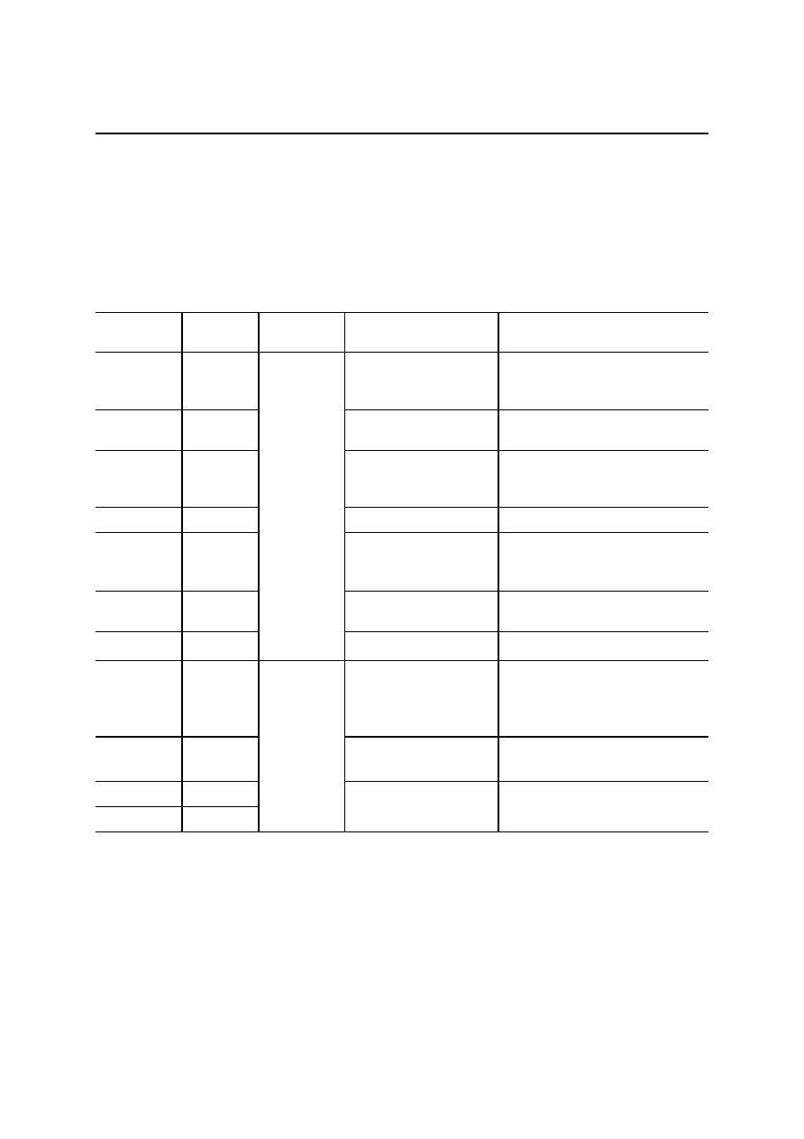
PIN DESCRIPTIONS
Table P1. List of pins and their descriptions
Pin Symbol
I/O
Type
Description
27
DISP
O
4mA drive
LCD Display enable
28
DF
O
4mA drive
LCD AC driving signal pin
29
FRP
O
4mA drive
LCD Frame pulse
30
LCP
O
4mA drive
LCD Line clock pulse
32-35
DDA3 - 0
O
4mA drive
3-state
LCD Data A
37
CPS
O
4mA drive
LCD Data clock pulse 2 or Data Strobe
38
CP
O
4mA drive
LCD Data clock pulse
42-45
DDB3 - 0
O
4mA drive
3-state
LCD Data B
47-50
DDC3 - 0
O
4mA drive
3-state
LCD Data C
52-55
DDD3 - 0
O
4mA drive
3-state
LCD Data D
59, 60
PORT0, 1
I/O
LVTTL /
4mA drive
General purpose I/O port (input / output direction
can be set for each pin)
62, 64, 65
A18 - 16
I
LVTTL
Host address bus
66, 67, 70, 71
73, 74, 76-79
81-84, 86, 87
AD15 - 00
I/O
LVTTL /
4mA drive
Host address/data multiplexed bus
92-95, 97-100
D07 - 00
I/O
LVTTL /
4mA drive
Host data bus
2 CSN
I
LVTTL, Schmitt Chip select (active "L")
3 REN
I
LVTTL, Schmitt Read enable (active "L")
4 WEN
I
LVTTL, Schmitt Write enable (active "L")
5 BSN
I
LVTTL, Schmitt Bus start/address strobe (active "L")
7 DSN
I
LVTTL, Schmitt Data strobe (active "L")
8 BSYN
O
8mA drive
3-state
Busy/wait (active "L", 3-stated)
10 BCLK
I
LVTTL, Schmitt Bus clock
9 REGS
I
LVTTL, Schmitt Register select
12
XOSCI
I
Clock oscillator input (built-in feedback resistor)
14 XOSCO
O
X'tal oscillation
buffer
Clock oscillator output
16 RESETN
I
LVTTL
System reset (active "L")
18, 19, 21, 22
HMOD3 - 0
I
LVTTL
Host mode select
23, 24
TEST1, 0
I
LVTTL
Test mode select (normally tied to "L")
58
(TOUT)
O
2mA drive
(Test output. Not used.)
11, 20, 61, 68,
85, 96
VDDI
--
Power Supply
Power supply for the internal core and I/O
36, 46
VDDO
--
Power Supply
Power supply for the LCD interface signal outputs
6, 15, 31, 40,
56, 63, 80, 88
VSS
--
Power Supply
Common ground

FEDL87V3104-03
OKI Semiconductor
ML87V3104
5/69
FUNCTIONAL DESCRIPTION
1. Display Memory
The address and data configuration of the display memory is specified by making control register settings.
When the defined memory size is smaller than the internal DRAM (4M bits), the page mode operation is started
automatically, making it possible to specify the display address in units of a page and to access the host CPU (a
maximum of 256 pages). Even when the address space of the host CPU bus is smaller than the display memory
space, the entire area can be accessed using the page mode.
There are limitations on the LCD drive mode depending on the display memory data width. (See Section 3.1.)
Note that the LCD control timings must be defined before accessing the display memory. (See Section 3.1.2)
� Control registers:
IMASZX [#03h: bit 3-0]: Display memory horizontal size (2
n
) (Table F1.1)
IMASZY [#03h: bit 7-4]: Display memory vertical size (2
n
)
(Table F1.1)
IMDBPP [#02h: bit 1-0]: Number of bits per pixel
(Table F1.2)
HSTPGA [#3Bh]:
Page number for host access
Table F1.1 Display memory size selection
IMASZY
Vertical size
(lines)
IMASZX
Horizontal size
(pixels)
0000 64
0000 64
0001
128
0001
128
0010
256
0010
256
0011
512
0011
512
0100
1024 0100
1024
0101
2048 0101
2048
0110
4096 0110
4096
0111 (Reserved)
0111 (Reserved)
1XXX (Reserved)
1XXX (Reserved)
Table F1.2 Display memory data width
Number of simultaneously displayed colors
IMDBPP
Number of bits
(bits / pixel)
Color mode
Monochrome mode
Applicable
LCD type
00X --
--
--
--
010 4
16/4096 16
011 8
Pseudo color
256/4096 256
STN/TFT
4096
--
STN
100 16*
1
Direct
color
65536 --
TFT
*1: Correspondence between the display memory data and the color data in the 16BPP mode.
Upper byte
Lower byte
R
0
R
3
R
2
R
1
B
0
B
3
B
2
B
1
G
3
G
2
G
1
G
0
7
0
0
7
Upper byte
Lower byte
R
5
R
4
R
3
R
2
R
1
B
5
B
4
B
3
B
2
B
1
G
5
G
4
G
3
G
2
G
1
G
0
7
0
0
7
STN 16 BPP
TFT 16 BPP
(12)
(no use)

FEDL87V3104-03
OKI Semiconductor
ML87V3104
6/69
Example 1: When IMASZX = "100", IMASZY = "100", and IMDBPP = "010":
The memory size is 1024 horizontal pixels, 1024 vertical lines and 4 bits/pixel.
1024
� 1024 � 4 = 4M bits
The memory can be accessed using 19 host address bits (10 horizontal bits plus 9 vertical bits) with
the host data width being 8 bits (in 2-pixel packed format).
Example 2: When IMASZX = "010", IMASZY = "010", and IMDBPP = "011":
The memory size is 256 horizontal pixels, 256 vertical lines with 8 bits/pixel and 8 pages.
256
� 256 � 8 = 512K bits (< 4M bits)
4M bits/512 K bits = 8 pages
The memory can be accessed using 16 host address bits (8 horizontal bits plus 8 vertical bits) and the
lower 3 bits of the page register, with the host data width being 8 bits (in 2-pixel packed format).

FEDL87V3104-03
OKI Semiconductor
ML87V3104
7/69
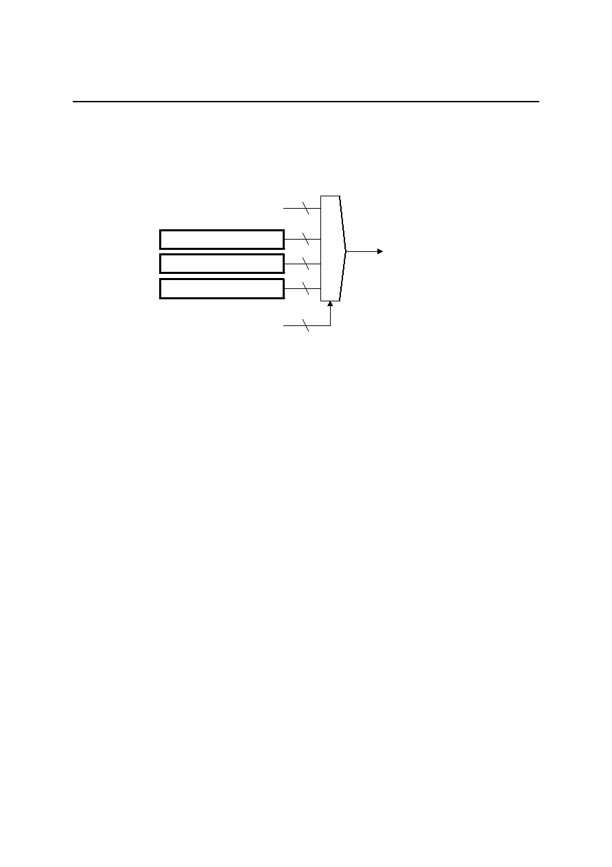
2. Display Control
2.1 Display
section
The display section of the ML87V3104 is composed of the display memory, the cursor and cursor color registers,
the color palette, the FRC table, and output format conversion section. (Fig. F2.1)
The color display in the case of 4 bits/pixel and 8 bits/pixel can be made using, respectively, 16 and 256 colors out
of 4096 colors. (Pseudo-color mode)
Further, in the STN mode, the output is made after conversion into the gradation expression data in the FRC
method.
In the case of 16 bits/pixel, the output is made directly without passing through the color palette. (Direct color
mode)
In the STN mode, out of the total 16 bits, only 4 bits each of RGB (12 bits in all) will be valid and display 4096
colors can be made.
In the TFT mode, the 16 bits are divided into 5 bits of R, 6 bits of G, and 5 bits of B, making it possible to display
65536 colors.
Even the direct mode can also be used in the case of 8 bits/pixel.
SEL
Output
format
conversion
SEL
8/16
4
DDA3-0
DDB3-0
DDC3-0
DDD3-0
SEL
4
SEL
4
4
FRC
Table
16
�
16b
1
1
1
Color
palette
256
�
12b
4
4
4
8
Color
register
3
�
8b
8
8/16
Cursor
pattern
register
16
�
16
�
2b
2
Cursor
display
control
Display memory
512
�
8b
Fig. 2.1 The display section

FEDL87V3104-03
OKI Semiconductor
ML87V3104
8/69
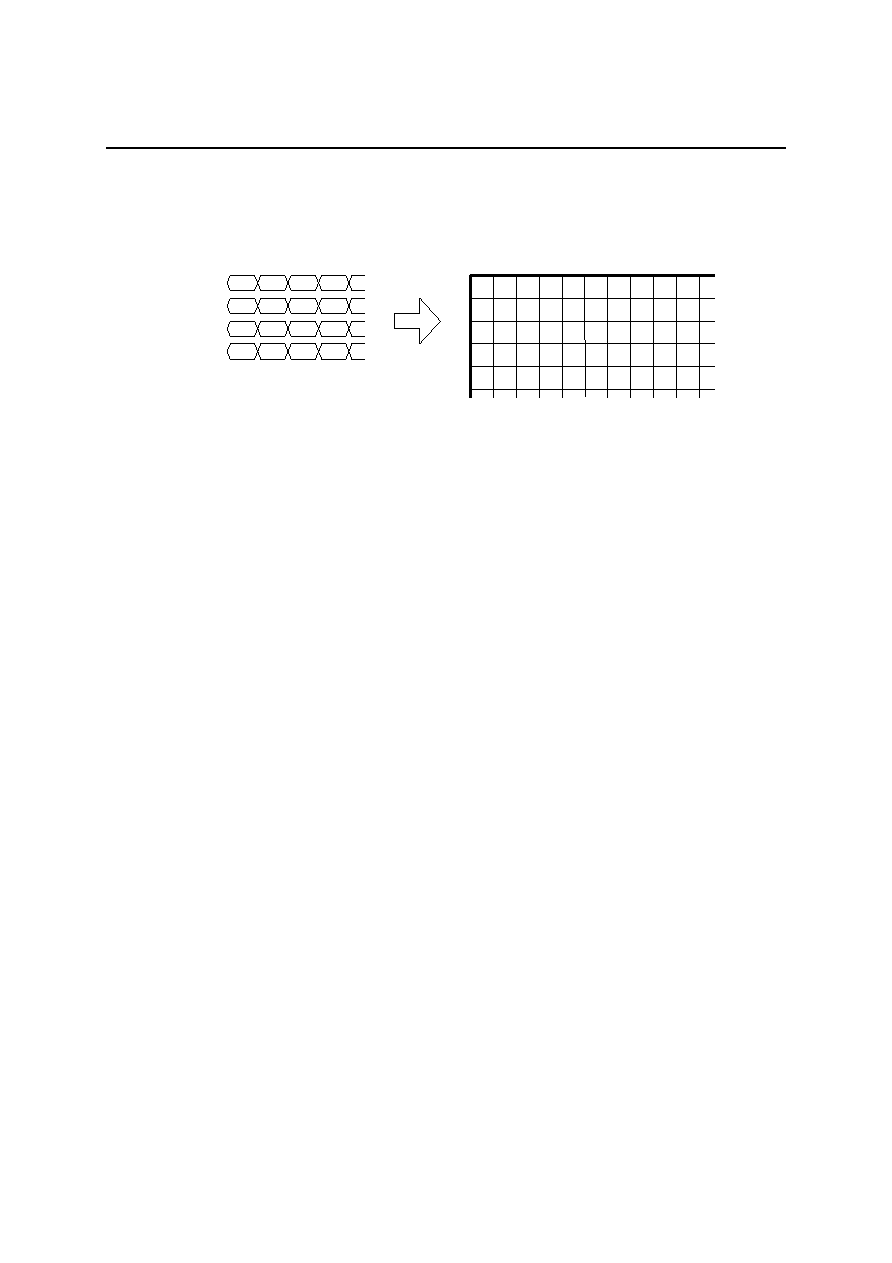
2.2 Display screen composition
The display screen consists of the main screen with a size equal to the display size of the LCD panel, and a
sub-screen displayed in a smaller area within the main screen. (Fig. F2.2.1)
In the case of a color LCD panel, one set of the three colors (RGB) is considered as one pixel. (Fig. F2.2.2)
(3)
(1)
(2)
(4)
Main screen
Sub-screen
(5)
(6)
Fig. F2.2.1 The display screen composition
(a) Monochrome LCD
(b) Color LCD
1 Line
1 Pixel
1 Line
1 Pixel
Fig. F2.2.2 The LCD panel dot composition
�
Control registers:
(1) MSCSZH [#21h, #20h]: Horizontal display size
1024 pixels
(2) MSCSZV
[#23h, #22h]: Vertical display size
1024 lines
(3) SSCSZH
[#25h, #24h]: Sub-screen horizontal display size < (1)
(4) SSCSZV
[#27h, #26h]: Sub-screen vertical display size < (2)
(5) SDPOSH
[#29h, #28h]: Sub-screen horizontal display position < (1)
(6) SDPOSV [#2Bh, #2Ah]: Sub-screen vertical display position < (2)

FEDL87V3104-03
OKI Semiconductor
ML87V3104
9/69
2.3 Display
functions
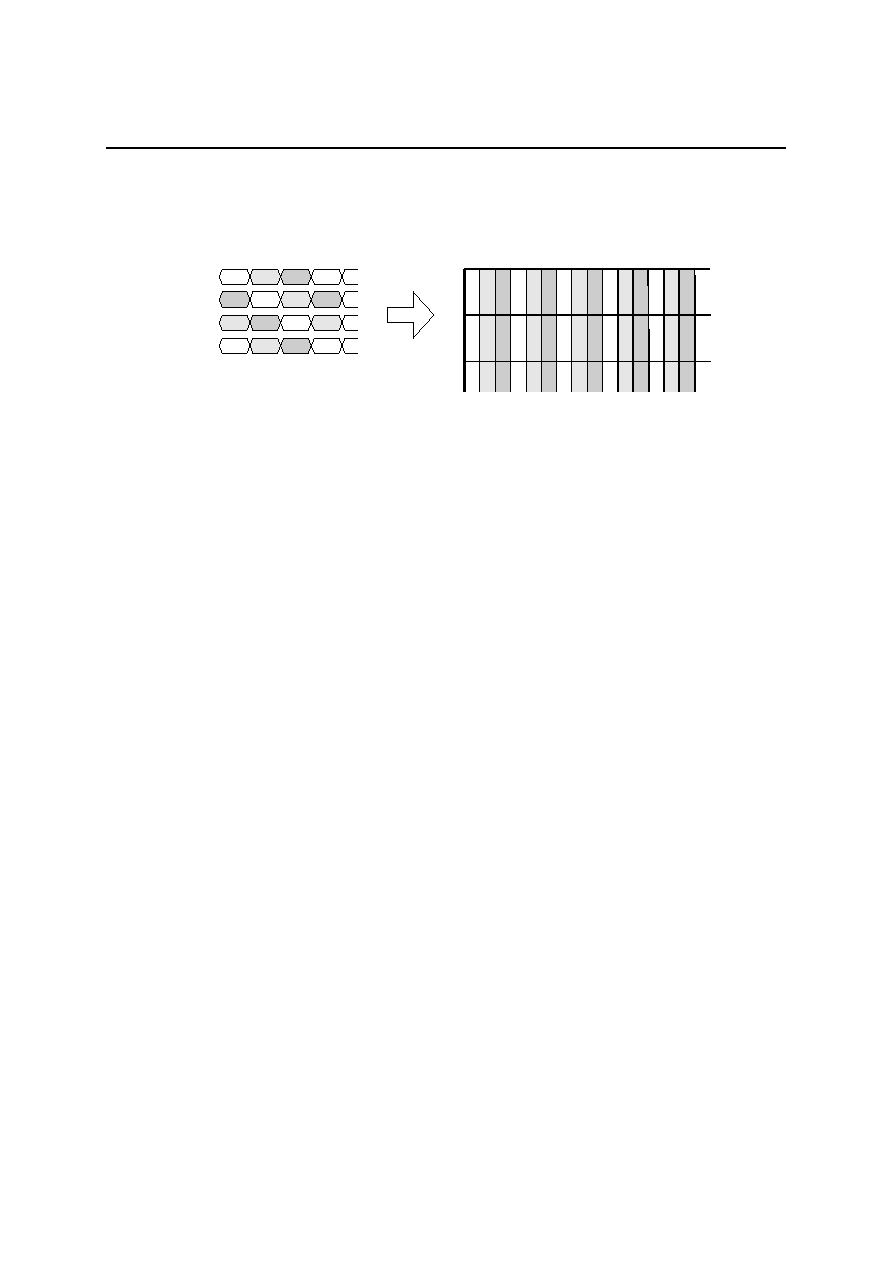
2.3.1 Main screen, sub-screen, and scrolling
The main screen and the sub-screen in the display screen (see Fig. F2.2.1) can respectively display the areas
specified in the display memory. (Fig. F2.3.1)
(3)
(1)
(2)
(4)
Main screen
Sub-screen
Display memory
Origin
LCD Screen
Fig. F2.3.1 The display screen composition
�
Control registers:
(1) MDPSTX [#31h, #30h]:
Starting horizontal address of reading out the main screen display area
(2) MDPSTY [#33h, #32h]:
Starting vertical address of reading out the main screen display area
(3) SDPSTX [#35h, #34h]:
Starting horizontal address of reading out the sub-screen display area
(4) SDPSTY [#37h, #36h]:
Starting vertical address of reading out the sub-screen display area
(5) MDPPGA [#38h]:
Page number of the main screen display area
(6) SDPPGA [#39h]:
Page number of the sub-screen display area
The starting addresses of reading out the display memory can be specified for the separate main screen and
sub-screen in units of 16 horizontal pixels and one vertical line. In addition, by successively over-writing by the
host CPU, it is possible to realize scrolling of the display screen.
The sub-screen is always displayed by superimposing on the main screen.
FEDL87V3104-03
OKI Semiconductor
ML87V3104
10/69
2.3.2 Screen mode
It is possible to select the method of placing the LCD panel by setting the screen mode.
It is possible to specify the landscape (horizontal screen) or portrait (vertical screen), and to specify the left/right
and top/bottom reversal of the displayed image.
�
Control register:
SCRMOD [#02h; bit6-4]:
Screen mode
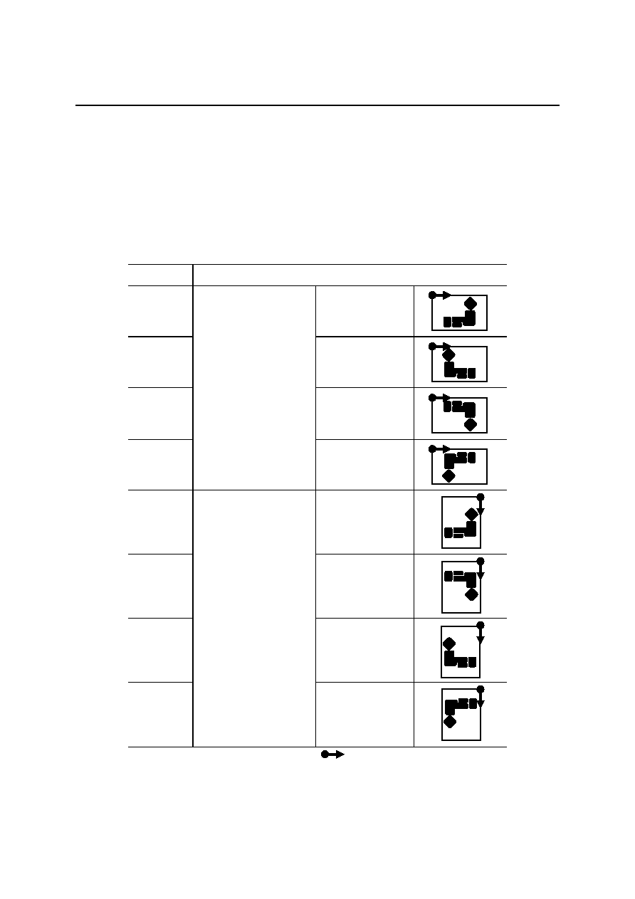
Table F2.3.2 The screen modes
SCRMOD Screen
mode
000
Normal
001
Left/right flip
010
Top/bottom flip
011
Landscape
(longer horizontal side)
Left/right and
top/bottom flip
100
Normal
101
Top/bottom flip
110
Left/right flip
111
Portrait
(longer vertical side)
Left/right and
top/bottom flip
Note: The screen mode definition has a difference between Landscape and Portrait.
: LCD data output scanning direction

FEDL87V3104-03
OKI Semiconductor
ML87V3104
11/69
2.4 Cursor
2.4.1 Cursor display
It is possible to display the cursor on the screen. It is also possible to select whether or not to display the cursor,
and when cursor display is selected, it is always displayed in the front-most screen. This LSI has a pattern register
for the display of a cursor with a size of 16 pixels
� 16 lines � 2 bits in which it is possible to write the cursor shape.
Displaying the cursor has no effect on the display memory.
The cursor display color can be specified by the contents of the 2-bit (4-value) cursor pattern register for each pixel.
One of the four values is "transparent", and that pixel is not displayed when this value is specified. The other 3
values respectively correspond to the 8-bit cursor color registers (CSCOL1 to CSCOL3), and the specified value is
converted to the actually displayed pixel data from the color palette common to the display memory output.
2.4.2 Cursor display position
The cursor display position is specified in terms of the position in the screen of the cursor origin (the top left corner
of the cursor).
(1)
(2)
LCD screen
Cursor
Fig. F2.4.2 The cursor position
�
Control registers:
(1) CSPOSH [#2Dh, #2Ch]: Cursor display horizontal position
(2) CSPOSV [#2Fh, #2Eh]: Cursor display vertical position
(3) CSDENB [#2Fh; bit7]:
Cursor display enable (`0': disable, `1': enable)
FEDL87V3104-03
OKI Semiconductor
ML87V3104
12/69
2.4.3 Cursor color register
The display data of the cursor is determined corresponding to the cursor data by the contents of the 8-bit cursor
color register. The number of valid bits depends on the number of bits per pixel (IMDBPP).
Cursor color register 1
To color palette
Display memory data
Cursor color register 2
Cursor color register 3
SEL
8
8
8
8
Cursor data
00
01
10
11
2
Fig. F2.4.3 The cursor color register
�
Control registers:
CSCOL1 [#1Dh]:
Cursor color register 1
CSCOL2 [#1Eh]:
Cursor color register 2
CSCOL3 [#1Fh]:
Cursor color register 3
Valid bits:
Bits 3 to 0 for 4BPP
Bits 7 to 0 for 8BPP

FEDL87V3104-03
OKI Semiconductor
ML87V3104
13/69
2.4.4 Cursor pattern register
The cursor pattern (shape) can be prepared by writing data in the 16 x 16 x 2-bit cursor pattern register. The data is
accessed in the 4-pixel packed format. (Fig. F2.4.4)
Y = 0
Y = 1
Y = 2
2 bits
X = 0 1 2 3 4 5 6 7 8
X = 4n + 0 X = 4n + 1 X = 4n + 2 X = 4n + 3
bit1 bit0 bit1 bit0 bit1 bit0 bit1
bit0
Register
data
bit7 bit6 bit5 bit4 bit3 bit2 bit1
bit0
16 pixels
16
lines
Cursor
Fig. F2.4.4 The cursor pattern register
�
Control registers:
CSPTAY [#18h; bit5-2]:
Cursor pattern register address Y (4 bits)
CSPTAX [#18h; bit1-0]:
Cursor pattern register address X (higher 2 bits)
CSPTD0 [#19h; bit7-6]:
Cursor pattern register data (X address = 4n+0)
CSPTD1 [#19h; bit5-4]:
Cursor pattern register data (X address = 4n+1)
CSPTD2 [#19h; bit3-2]:
Cursor pattern register data (X address = 4n+2)
CSPTD3 [#19h; bit1-0]:
Cursor pattern register data (X address = 4n+3)
FEDL87V3104-03
OKI Semiconductor
ML87V3104
14/69
2.5 Color
palette
The data written in the display memory is converted into the actual color data output to the LCD panel by the color
palette. (Pseudo-color mode) The color palette contains 4-bit
� 3-color (R, G, B) (= 12 bits) registers
corresponding to each of the 256 entries addresses.
The correspondence between the display memory data and the color palette entry is established as shown in Table
F2.5 depending on the data width of the display memory. The color palette cannot be used in the direct color mode
(16BPP).
Table F2.5 The display memory data vs. the color palette entries
Display memory data
*1
8 BPP
4 BPP
Color palette entry
00 0
00
01 1
01
02 2
02
03 3
03
04 4
04
05 5
05
06 6
06
07 7
07
08 8
08
09 9
09
0A A
0A
0B B
0B
0C C
0C
0D D
0D
0E E
0E
0F F
0F
10 --
10
11 --
11
12 --
12
13 --
13
14 --
14
FC --
FC
FD --
FD
FE --
FE
FF --
FF
*1: A hyphen "--" indicates that the data value is not used.
�
Control registers:
COLPTA [#10h]:
Color palette entry address
COLPDR [#11h; bit7-4]:
Color palette data R
COLPDG [#12h; bit7-4]:
Color palette data G
COLPDB [#13h; bit7-4]:
Color palette data B

FEDL87V3104-03
OKI Semiconductor
ML87V3104
15/69
2.6 Gray level control
In the case of an STN type LCD panel, the FRC (Frame Rate Control) method is used for the multiple gray level
display. By controlling the blinking pattern of the dot, it is possible to express intermediate gray levels in a quasi
manner.
Taking 16 frames as one period, it is possible to express up to 16 gray levels.
The dot blinking pattern is set in the 16-word x 16-bit FRC table. The 4-bit table address corresponds to the gray
levels from 0 to 15. The 16-bit table data expresses the dot blinking patterns corresponding to the different gray
levels, and the dot display is switched for each frame sequentially from the MSB to the LSB, with the operation
being repeated at a period of 16 frames.
In the case of a color STN panel, the FRC pattern is the same for all colors.
�
Control registers:
FRCTBA [#15h; bit3-0]:
FRC table address
FRCTBD [#17h, #16h]:
FRC table data
Table F2.6 The FRC table (initial value)
FRC table (displayed in the sequence 15, 14, ..., 1, 0)
Table
address
(gradation) 15 14 13 12 11 10
9 8 7 6 5 4 3 2 1 0
0
0 0 0 0 0 0 0 0 0 0 0 0 0 0 0 0
1
0 0 0 0 0 0 1
0 0 0 0 0 0 0 0 0
2
0 0 0 0 0 1
0 0 0 0 0 0 0 1
0 0
3
0 0 0 0 1
0 0 0 0 1
0 0 0 0 1
0
4
0 0 0 1
0 0 0 1
0 0 0 1
0 0 0 1
5 0
0
1
0 0 1
0 0 1
0 0 1
0 0 1
0
6 0
1
0 0 1
0 0 1
0
1
0 0 1
0 0 1
7
1
0
1
0
1
0
1
0
1
0
1
0 0 1
0 0
8 0
1
0
1
0
1
0
1
0
1
0
1
1
0
1
1
9
1
0
1
1
0
1
1
0
1
0
1
1
0
1
1
0
10
1
1
0
1
1
0
1
1
0
1
1
0
1
1
0
1
11
1
1
1
0
1
1
1
0
1
1
1
0
1
1
1
0
12
1
1
1
1
0
1
1
1
1
0
1
1
1
1
0
1
13
1
1
1
1
1
0
1
1
1
1
1
1
1
0
1
1
14
1
1
1
1
1
1
0
1
1
1
1
1
1
1
1
1
15
1
1
1
1
1
1
1
1
1
1
1
1
1
1
1
1
Note: This table shows the initial value set after a reset, and is not one assuming
any specific LCD panel specifications. Set the values in this table to suit
the characteristics of the LCD panel being used.
FEDL87V3104-03
OKI Semiconductor
ML87V3104
16/69
3. LCD Interface
3.1 LCD driving method
3.1.1 LCD driving mode
The ML87V3104 is suitable for various types of LCD panels, and allows the LCD driving mode to be selected by
setting the control registers.
The number of valid data bits in the LCD interface varies depending on the driving mode. The output data signals
that are not used will be maintained in the high-impedance state. Further, there are some restrictions on the
selection of the display memory data width (bits per pixel) depending on the driving mode. (Table F3.1)
�
Control registers:
LCDMOD [#00h; bit7-4]:
LCD panel operation mode
LCDDAT [#00h; bit3-0]:
LCD panel interface data width
Table F3.1 LCD driving modes
Output data
LCDMOD LCDDAT
LCD driving mode
DDA DDB DDC DDD
Display
memory BPP
000
4
bits O Z Z Z
010
8 bits
O
O
Z
Z
0000
100
Pseudo-color
4 bits,
2 phase
O Z Z Z
4, 8
000
4
bits O Z Z Z
010
8 bits
O
O
Z
Z
0001
100
Color STN
Direct color
4 bits,
2 phase
O Z Z Z
16(12)
000
4
bits O Z Z Z
010
8 bits
O
O
Z
Z
0100
100
Monochrome STN
4 bits,
2 phase
O Z Z Z
4
1000 000
Pseudo-color
12
bits O O O Z
4, 8
1001 001
Color TFT
Direct
color 16
bits O O O O
16
BPP: bits per pixel
`O': 4 bits are active.
`Z': 4 bits are in a high impedance state.

FEDL87V3104-03
OKI Semiconductor
ML87V3104
17/69
3.1.2 LCD control timing
The LCD control timing is determined by the LCP (line clock pulse) signal and the FRP (frame pulse) signal. It is
also possible to set the polarities of these pulses individually.
(7)
(2)
(3)
(1)
(5)
Active display area
(6)
LCP
FRP
Fig. F3.1.2 LCD drive timing
�
Control registers:
(1) LCPCYC [#05h, #04h]: (LCP signal period � 1)
In units of a CP clock in the STN color 4-bit mode
In units of 2 CP clocks in the STN color 8-bit mode or 4-bit 2-phase mode
In units of 4 CP clocks in the STN monochrome 4-bit mode
In units of 8 CP clocks in the STN monochrome 8-bit mode or 4-bit 2-phase mode
In units of a CP clock in the TFT color mode
(2) LCPSTA [#07h, #06h]: LCP start timing, in units of a CP clock
(3) LCPWID [#07h; bit7-4]: (LCP pulse width � 1), in units of 4
�
CP clocks
(4) LCPPOL [#05h; bit7]:
LCP pulse polarity, `0': Positive, `1': Negative
(5) FRPCYC [#09h, #08h]: FRP signal period, in units of a line, (5)
(6)+2
(6) FRPSTA [#0Bh, #0Ah]: FRP start timing, in units of a line
(7) FRPWID [#0Bh; bit7-4]: (FRP pulse width � 1), in units of a line
(8) FRPPOL [#09h; bit7]:
FRP pulse polarity, `0': Positive, `1': Negative
Note: The internal memory gets started by setting above registers. These must be set at first after the power
up or the internal memory cannot be accessed.
FEDL87V3104-03
OKI Semiconductor
ML87V3104
18/69
3.1.3 LCD AC driving signal DF
The toggle period of the DF signal (AC driving signal) can be specified to be either one frame period or the period
of the set number of lines.
�
Control registers:
DFFALT [#0Dh; bit7]:
DF signal toggle mode
DFLALT [#0Dh, #0Ch]:
(DF signal toggle period � 1), in units of a line
DFFALT
DF toggle mode
0
Reversal at one frame periods
1
Reversal at periods of (DFLALT+1) line
3.1.4 LCD data clocks CP, CPS
It is possible to select whether or not to output the CP and CPS clock pulses during the invalid period (blanking
period) of the LCD display data. In most cases, the appropriate setting is CPBLK = `1' for an STN LCD and
CPBLK = `0' for a TFT LCD.
�
Control register:
CPBLK
[#01h; bit7]:
Control of CP and CPS clock output during blanking
CPBLK
CP and CPS clock output during blanking
0 Active
1
Clock pulses are stopped

FEDL87V3104-03
OKI Semiconductor
ML87V3104
19/69
3.1.5 LCD data output control
Three types of control registers are provided in this LSI device for control of the LCD data output.
The register COLORD can be used for changing R, G, B sequence in a color LCD. This is also valid in the frame
sequential color mode.
The register DPDMOD is used for inverting the bits of the output data or for making the data all-zero or all-one.
The register DPMENB can be used for stopping the display memory readout operation itself. At this time, even
the LCD driving signals will be stopped. Further, it is also possible to specify the level of the DISP signal output.
The register REFENB controls the refresh operation of the display memory (embedded DRAM). If the refresh
operation is stopped, the entire contents of the display memory will be lost. Along with the register DPMENB, this
register is useful for achieving low power consumption when no display is being made.
�
Control registers:
COLORD [#01h; bit7]:
Color arrangement sequence of the color LCD panel
COLORD
Color arrangement sequence
0 0 0
R, G, B, R, G, B, � � �
0 0 1
G, B, R, G, B, R, � � �
0 1 0
B, R, G, B, R, G, � � �
1 0 1
R, B, G, R, B, G, � � �
1 1 0
G, R, B, G, R, B, � � �
1 1 1
B, G, R, B, G, R, � � �
DPDMOD [#01h; bit3-2]: LCD data display mode
DPDMOD
LCD data display mode
0 0
Normal
0 1
Reverse
1 0
All `0'
1 1
All `1'
DPMENB [#01h; bit1-0]: Display memory readout control, definition of DISP signal output
DPMENB
Display memory readout
DISP signal
0 0
Memory readout stopped
DISP = `L'
0 1
LCD drive stopped
DISP = `H'
1 0
Memory readout operating
DISP = `L'
1 1
LCD drive operating
DISP = `H'
REFENB [#02h, bit7, 3]: Embedded DRAM refresh operation enable
REFENB
1 0
DRAM refresh operation
0
X
Fully stopped (sleep mode)
*1
0
Operation only during blanking
1
1 Always
operating
*1: The contents of the display memory will be lost in the sleep mode.

FEDL87V3104-03
OKI Semiconductor
ML87V3104
20/69
3.1.6 Calculation of the display frame rate
The frame rate (the frame frequency) is determined by the periods of the LCD panel driving signals LCP and FRP,
the clock frequency, and the LCD driving mode.
Frame rate = FXOSC/{(FRPCYC)
�
(LCPCYC)
�
(TPX)}
Where,
FXOSC : External input clock frequency,
FRPCYC : Period (in units of a line) of the FRP (frame pulse) signal,
LCPCYC : Period (in units of a pixel) of the LCP (line pulse) signal,
TPX : TPX = 3/4 in the case of a color STN type LCD and TPX = 1 in all other cases.
Example: What is the input clock frequency for making the frame rate equal to 150 Hz in the case of a color
STN QVGA (320
� 240) type LCD panel?
FRPCYC = 240 + 2 = 242
LCPCYC = 320 + 40 = 360
FXOSC = 150
�
242
�
360
�
3/4 = 9.8 MHz

FEDL87V3104-03
OKI Semiconductor
ML87V3104
21/69
3.2 LCD data output format
The valid output data signal and the data format are determined depending on the LCD driving mode.
3.2.1 Color STN, 4-bit mode
LCD panel segment arrangement
LCD data output sequence
R0
G0
B0
R1
G1
B1
R2
G2
B2
R3
G3
B3
R4
G4
B4
R5
DDA 3
DDA2
DDA1
DDA0
R
0
G
0
B
0
R
1
G
1
B
1
R
2
G
2
B
2
R
3
G
3
B
3
Fig. F3.2.1 Color STN, 4-bit mode
3.2.2 Color STN, 8-bit mode
LCD panel segment arrangement
LCD data output sequence
DDA 3
DDA2
DDA1
DDA0
DDB 3
DDB2
DDB1
DDB0
R0
G0
B0
R1
G1
B1
R2
G2
B2
R3
G3
B3
R4
G4
B4
R5
R
0
G
0
B
0
R
1
G
1
B
1
R
2
G
2
B
2
R
3
G
3
B
3
Fig. F3.2.2 Color STN, 8-bit mode
FEDL87V3104-03
OKI Semiconductor
ML87V3104
22/69
3.2.3 Color STN, 4-bit 2-phase mode
LCD panel segment arrangement
LCD data output sequence
R0
G0
B0
R1
G1
B1
R2
G2
B2
R3
G3
B3
R4
G4
B4
R5
DDA 3
DDA2
DDA1
DDA0
R
0
G
0
B
0
R
1
G
1
B
1
R
2
G
2
B
2
R
3
G
3
B
3
Fig. F3.2.3 Color STN, 4-bit, 2-phase mode

FEDL87V3104-03
OKI Semiconductor
ML87V3104
23/69
3.2.4 Monochrome STN, 4-bit mode
LCD panel segment arrangement
LCD data output sequence
DDA 3
DDA2
DDA1
DDA0
0
1
2
3
4
5
6
7
8
9
10
11
12
13
14
15
0
1
2
3
4
5
6
7
8
9
Fig. F3.2.4 Monochrome STN, 4-bit mode
3.2.5 Monochrome STN, 8-bit mode
LCD panel segment arrangement
LCD data output sequence
0
1
2
3
4
5
6
7
8
9
DDA 3
DDA2
DDA1
DDA0
0
1
2
3
4
5
6
7
8
9
10
11
12
13
14
15
DDB 3
DDB2
DDB1
DDB0
Fig. F3.2.5 Monochrome STN, 8-bit mode
FEDL87V3104-03
OKI Semiconductor
ML87V3104
24/69
3.2.6 Monochrome STN, 4-bit 2-phase mode
LCD panel segment arrangement
LCD data output sequence
DDA 3
DDA2
DDA1
DDA0
0
1
2
3
4
5
6
7
8
9
10 11
12 13
14 15
0
1
2
3
4
5
6
7
8
9
Fig. F3.2.6 Monochrome STN, 4-bit, 2-phase mode

FEDL87V3104-03
OKI Semiconductor
ML87V3104
25/69
3.2.7 Color TFT, 12-bit mode
LCD panel segment arrangement
LCD data output sequence
R
0
G
0
B
0
R
1
G
1
B
1
R
2
G
2
B
2
R
3
G
3
B
3
B0
B1
B2
B3
DDC3-0 (B)
G0
G1
G3
G2
DDB3-0 (G)
R0
R2
R3
R1
DDA
3-0 (R)
Fig. F3.2.7 Color TFT, 12-bit mode
3.2.8 Color TFT, 16-bit mode
LCD panel segment arrangement
LCD data output sequence
R
0
G
0
B
0
R
1
G
1
B
1
R
2
G
2
B
2
R
3
G
3
B
3
B0
B1
B2
B3
DDC0 (B)
DDD3-0
G0
G1
G3
G2
DDB2-0 (G)
DDC3-1
R0
R2
R3
R1
DDA
3-0 (R)
DDB3
Fig. F3.2.8 Color TFT, 16-bit mode

FEDL87V3104-03
OKI Semiconductor
ML87V3104
26/69
4. General Purpose I/O Port
The ML87V3104 has two general purpose ports (PORT1, PORT0). It is possible to specify the input/output
directions independently for these ports. The output level of the output port can be set by writing data in the data
register. Further, the input level of the input port can be read out from the data register. When set as an input port,
writing to the data register will not be valid.
�
Control registers:
PTDDIR [#0Eh; bit1-0]:
General purpose port input/output mode (`0': output, `1': input)
PTDREG [#0Fh; bit1-0]:
General purpose port data register (`0': L level, `1': H level)
Bit 1 corresponds to PORT1 and bit 0 corresponds to PORT0.
PTDDIR[n] PORTn
0 Output
PTDREG[n]
PORTn
1 Input
PTDREG[n]
PORTn
Pin 59
PTDREG[0]
PTDDIR[0]
PORT0
Host Data
Pin 60
PTDREG[1]
PTDDIR[1]
PORT1
Host Data
Fig. F4.1 General purpose ports
FEDL87V3104-03
OKI Semiconductor
ML87V3104
27/69
5. Host Interface
5.1 Host interface bus mode selection
The host interface bus can be selected to suit the external bus modes of different types of CPUs by setting the pins
HMOD3 to HMOD0.
Table F5.1 Host interface bus mode
HMOD
[3:0]
Bus type
Address/
data bus
Bus control
Applicable CPUs
*1
0000 A0
CSN, WEN, REN,
Busy
Hitachi SH-1,2, H8S,
Fujitsu F
2
MC-16F, FR30
Toshiba TLCS-900/H2
0001 A1
AS, WEN, REN,
Busy
Hitachi SH-4
0010 A2
BSN, WEN, REN,
ACK
Hitachi SH-3,
Motorola MCF5204
Toshiba TX39
0011 --
(Reserved)
--
0100 A4
BSN, RWN, DSN,
ACK
Toshiba TX19,
Motorola MCF5206,
MPC801/850, M68K
0101 A5
BSN, RWN, DSN,
Busy
Mitsubishi M32R, NEC V830,
Intel SA-110
011X --
Separate
A[18:00]
D[07:00]
(Reserved) --
1000 B0
ASN, WEN, REN,
Busy
Hitachi SH-1,2,
NEC V850, 78K/IV
Mitsubishi M16C
Oki MSM66K, 80C51
1001 B1
AS, WEN, REN,
Busy
Fujitsu F
2
MC-16L,
Toshiba TLCS-900
101X --
11XX --
Multiplexed
A[18:16]
AD[15:00]
(Reserved) --
*1: The types of CPUs listed here are only for reference. Please examine well about the specifications
of the host interface signals and the timings of the MCU being used, and then select the host mode.

FEDL87V3104-03
OKI Semiconductor
ML87V3104
28/69
5.1.1 Bus control signals
The assignment of the bus control signals to the input/output pins is determined by the host interface bus mode.
Table F5.5.1 Bus control signals
Bus type
Pin name
A0 A1 A2 A4 A5 B0 B1
A18-16 A18-16 A18-16 A18-16 A18-16 A18-16 A18-16 A18-16
AD15-00 A15-00 A15-00 A15-00 A15-00 A15-00 AD15-00
AD15-00
D07-00 D07-00 D07-00 D07-00 D07-00 D07-00
--
--
REGS REGS REGS REGS REGS REGS REGS REGS
CSN CSN CSN CSN CSN CSN CSN CSN
REN REN REN REN RWN RWN REN REN
WEN WEN WEN WEN --
-- WELN WELN
BSN
-- BS BSN BSN BSN ASN AS
DSN -- -- -- -- --
WEHN
WEHN
BSYN BSYN BSYN ACK ACK BSYN BSYN BSYN
BCLK BCLK BCLK BCLK BCLK BCLK BCLK BCLK
REGS:
Memory/register address space selection; `L': memory, `H': register
CSN:
Chip select (Active `L')
REN:
Read enable (Active `L')
WEN:
Write enable (Active `L')
WEHN:
Higher byte write enable (Active `L')
WELN:
Lower byte write enable (Active `L')
RWN:
Read/write selection; `L': write, `H': read
BSN:
Bus start (Active `L')
ASN:
Address strobe (Active `L')
DSN:
Data strobe (Active `L')
BSYN:
Bus busy or wait (Active `L')
ACK:
Data acknowledge (Active `L')
BCLK: Bus
clock

FEDL87V3104-03
OKI Semiconductor
ML87V3104
29/69
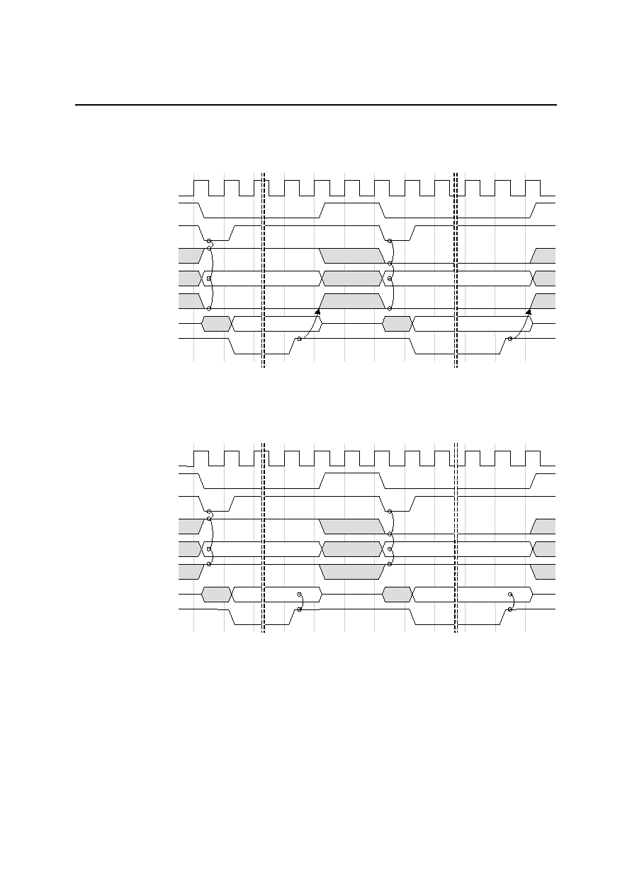
5.1.2 Bus interface timings
[Type A0 Write]
[Type A0 Read]
REN
(read)
(z)
MEM
BCLK
CSN
A18-00
REG
REGS
D7-0
BSYN
MEM
BCLK
CSN
A18-00
REG
REGS
WEN
D7-0
BSYN
(write)
(z)

FEDL87V3104-03
OKI Semiconductor
ML87V3104
30/69
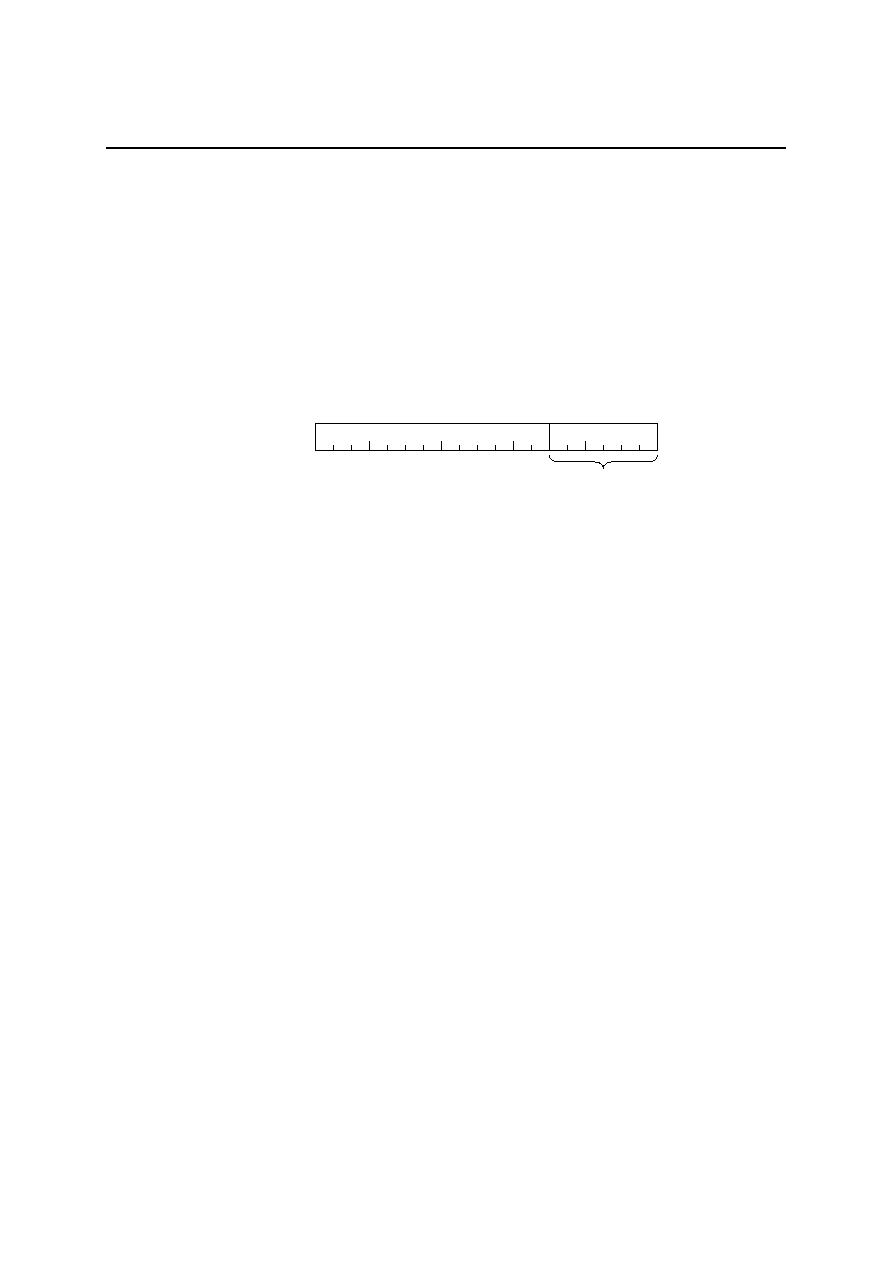
[Type A1 Write]
MEM
BCLK
CSN
A18-00
REG
REGS
WEN
D7-0
BSYN
(write)
(z)
BS
[Type A1 Read]
REN
(read)
(z)
MEM
BCLK
CSN
A18-00
REG
REGS
D7-0
BSYN
BS

FEDL87V3104-03
OKI Semiconductor
ML87V3104
31/69
[Type A2 Write]
MEM
BCLK
CSN
A18-00
REG
REGS
WEN
D7-0
ACK
(write)
(z)
BSN
[Type A2 Read]
MEM
BCLK
CSN
A18-00
REG
REGS
REN
D7-0
ACK
(read)
(z)
BSN

FEDL87V3104-03
OKI Semiconductor
ML87V3104
32/69
[Type A4 Write]
MEM
BCLK
CSN
A18-00
REG
REGS
RWN
D7-0
ACK
(write)
(z)
BSN
[Type A4 Read]
MEM
BCLK
CSN
A18-00
REG
REGS
D7-0
ACK
(read)
(z)
BSN
RWN
FEDL87V3104-03
OKI Semiconductor
ML87V3104
33/69
[Type A5 Write]
MEM
BCLK
CSN
A18-00
REG
REGS
D7-0
(write)
BSYN
(z)
BSN
RWN
[Type A5 Read]
MEM
BCLK
CSN
A18-00
REG
REGS
D7-0
(read)
BSYN
(z)
BSN
RWN

FEDL87V3104-03
OKI Semiconductor
ML87V3104
34/69
[Type B0 Write]
BCLK
CSN
A18-16
REGS
AD15-0
D (write)
BSYN
(z)
ASN
A
D (write)
A
WEHN
WELN
[Type B0 Read]
BCLK
CSN
A18-16
REGS
AD15-0
BSYN
ASN
REN
(z)
A
A
D
(read)
D
(read)

FEDL87V3104-03
OKI Semiconductor
ML87V3104
35/69
[Type B1 Write]
BCLK
CSN
A18-16
REGS
AD15-0
BSYN
AS
WEHN
WELN
MEM
D (write)
(z)
A
D (write)
A
[Type B1 Read]
BCLK
CSN
A18-16
REGS
AD15-0
BSYN
AS
REN
MEM
(z)
A
A
D
(read)
D
(read)

FEDL87V3104-03
OKI Semiconductor
ML87V3104
36/69
5.2 Address
mapping
The ML87V3104 supports a 19-bit byte address for access from the host CPU. The 4M bit display memory and
the 32-byte control registers are mapped to this address.
When accessing the display memory, the bit assignment of the address is determined by the setting of the memory
size. (Fig. F5.2) See the next section for details of the control registers.
7
Host address
0 18
0
7
0
Page No.
Host data
4 bits/pixel
8 bits/pixel
16 bits/pixel
X=2n+0 X=2n+1
X
1
Y
0
px0
px1
2-pixel packed format
Y address
(v bits)
X address
((u-1) bits)
Effective page No.
(w bits)
7 0 18
0
7
0
X
0
Y
0
px
0
7
Y address
(v bits)
X address
(u bits)
Effective page No.
(w bits)
7 0 18
0
7
0
X
0
Y
0
B
R
1
2
3
5
B
Byte
address
Y address
(v bits)
X address
(u bits)
Effective page No.
(w bits)
B='0'
B='1'
5
0
G
G
1
5
7 0 18
0
7
0
3
3
0
0
The number of total address bits = ( w bits ) + ( v bits ) + ( u bits ) = 19 bits (512K Byte)
Fig. F5.2 Display memory address mapping
FEDL87V3104-03
OKI Semiconductor
ML87V3104
37/69
5.3 Control
registers
5.3.1 Outline of control registers
The initial setting and the operation of the ML87V3104 are controlled by writing data from the host CPU in the
control registers.
There are 64 single-byte control registers, and in addition, a register space is provided by indirect addressing for
the color palette table (256
� 3 bytes), the FRC table (16 � 2 bytes), and the cursor pattern register (64 bytes). (See
Table F5.1)
The control registers can be accessed by the host CPU by taking the REGS signal input to the `H' level.
18
15
11
7
5
0
Host address
x x
x
Control register
address (6 bits)
x
x
x
x
x
x
x
x
x
x
Fig. F5.3 The control register address

FEDL87V3104-03
OKI Semiconductor
ML87V3104
38/69
Table F5.1 List of control registers (part 1/2)
Register name
*1
Register
address
bit 7 bit 6 bit 5 bit 4 bit 3 bit 2 bit 1 bit 0
Function
00 LCDMOD
(Res)
LCDDAT
LCD driving mode
01
CP
BLK
COLORD
DPDMOD
DPMENB
Display operation mode
02
REF
ENB1
SCRMOD
REF
ENB0
IMDBPP
Memory operation mode
03 IMASZY IMASZX
Display
memory
size
04 LCPCYC[7:0]
05
LCP
POL
(Reserved) LCPCYC[10:8]
LCP (line) period and polarity
06 LCPSTA[7:0]
07 LCPWID
(Res)
LCPSTA[10:8]
LCP start position, pulse width
08 FRPCYC[7:0]
09
FRP
POL
(Reserved) FRPCYC[10:8]
FRP (frame) period and polarity
0A FRPSTA[7:0]
0B FRPWID
(Res)
FRPSTA[10:8]
FRP start position, pulse width
0C DFLALT[7:0]
0D
DFF
ALT
(Reserved) DFLALT[10:8]
DF (AC driving signal) toggle period
(1 frame or n lines)
0E
(Reserved)
PTDDIR
General purpose port I/O mode
0F
(Reserved)
PTDREG
General purpose port data register
10
COLPTA[7:0]
Color palette table address
11
COLPDR[3:0]
(Reserved)
Color palette table data R
12
COLPDG[3:0]
(Reserved)
Color palette table data G
13
COLPDB[3:0]
(Reserved)
Color palette table data B
14 (Reserved)
(Reserved)
15 (Reserved) FRCTBA[3:0]
FRC
table
address
16 FRCTBD[7:0]
17 FRCTBD[15:8]
FRC table data
18
(Res)
CSPTAY[3:0]
CSPTAX[3:2] Cursor pattern register address
19
CSPTD0 CSPTD1 CSPTD2 CSPTD3
Cursor pattern register data
1A (Reserved)
(Reserved)
1B (Reserved)
(Reserved)
1C (Reserved)
(Reserved)
1D
CSCOL1[7:0]
Cursor color register 1
1E
CSCOL2[7:0]
Cursor color register 2
1F
CSCOL3[7:0]
Cursor color register 3
*1: The entries "(Reserved)" or "(Res)" indicate reserved bits. Writing data to these bits is not valid and
the data read out from these bits will be indeterminate.
FEDL87V3104-03
OKI Semiconductor
ML87V3104
39/69
Table F5.1 List of control registers (part 2/2)
Register name
*1
Register
address
bit 7 bit 6 bit 5 bit 4 bit 3 bit 2 bit 1 bit 0
Function
20 MSCSZH[7:0]
21 (Reserved)
[9:8]
Main screen horizontal size
22 MSCSZV[7:0]
23 (Reserved)
[9:8]
Main screen vertical size
24 SSCSZH[7:0]
25 (Reserved)
[9:8]
Sub-screen horizontal size
26 SSCSZV[7:0]
27 (Reserved)
[9:8]
Sub-screen vertical size
28 SDPOSH[7:0]
29 (Reserved)
[9:8]
Sub-screen display horizontal position
2A SDPOSV[7:0]
2B
SSD
ENB
(Reserved) [9:8]
Sub-screen display vertical position
Sub-screen display enable
2C CSPOSH[7:0]
2D (Reserved)
[9:8]
Cursor display horizontal position
2E CSPOSV[7:0]
2F
CSD
ENB
(Reserved) [9:8]
Cursor display vertical position
Cursor display enable
30 MDPSTX[7:0]
31 (Reserved)
MDPSTX[11:8]
Display memory horizontal position for
main screen
32 MDPSTY[7:0]
33 (Reserved)
MDPSTY[11:8]
Display memory vertical position for
main screen
34 SDPSTX[7:0]
35 (Reserved) SDPSTX[11:8]
Display memory horizontal position for
sub-screen
36 SDPSTY[7:0]
37 (Reserved) SDPSTY[11:8]
Display memory vertical position for
sub-screen
38 MDPPGA[7:0]
Display memory page number for main
screen
39 SDPPGA[7:0]
Display memory page number for
sub-screen
3A (Reserved)
(Reserved)
3B HSTPGA[7:0]
Display memory page number for host
access
3C (Reserved)
3D (Reserved)
3E (Reserved)
3F (Reserved)
(For testing, cannot be written into)
*1: The entries "(Reserved)" or "(Res)" indicate reserved bits. Writing data to these bits is not valid and the data
read out from these bits will be indeterminate.

FEDL87V3104-03
OKI Semiconductor
ML87V3104
40/69
5.3.2 Register details
In the following descriptions of the different registers, the underlined part indicates the initial value after a reset.
[#00h] LCD driving mode
Data bit
bit 7
bit 6
bit 5
bit 4
bit 3
bit 2
bit 1
bit 0
LCDMOD LCDDAT
Register
3 2 1 0
(Reserved)
2 1 0
W/R W/R --
W/R
�
LCDMOD[3:0]:
LCD panel operation mode selection
�
LCDDAT[2:0]:
LCD panel interface data width selection
LCDMOD LCDDAT
LCD
Driving
mode
000 4-bit
mode
010 8-bit
mode
0000
100
Color STN
4-bit 2-phase mode
0010 XXX
(Reserved)
--
000 4-bit
mode
010 8-bit
mode
0100
100
Monochrome STN
4-bit 2-phase mode
0110 XXX
(Reserved)
--
1000 000
12-bit
mode (pseudo-color)
1001 001
Color TFT
16-bit mode (direct color)
11XX XXX
(Reserved)
--
`X': Don't care

FEDL87V3104-03
OKI Semiconductor
ML87V3104
41/69
[#01h] Display operation mode
Data bit
bit 7
bit 6
bit 5
bit 4
bit 3
bit 2
bit 1
bit 0
COLORD DPDMOD
DPMENB
Register
CP
BLK
2 1 0 1 0 1 0
W/R W/R
W/R
W/R
W/R
�
CPBLK:
Control of CP clock output during blanking
CPBLK
CP Output during blanking
0 Active
1
Fixed at CP = `L', CPS = `H'
�
COLORD[2:0]: Color arrangement sequence of color LCD panel
COLORD[2:0]
Color arrangement sequence
0 0 0
R, G, B, R, G, B, � � �
0 0 1
G, B, R, G, B, R, � � �
0 1 0
B, R, G, B, R, G, � � �
0 1 1
(Reserved)
1 0 0
(Reserved)
1 0 1
R, B, G, R, B, G, � � �
1 1 0
G, R, B, G, R, B, � � �
1 1 1
B, G, R, B, G, R, � � �
�
DPDMOD[1:0]: LCD data display mode
DPDMOD[1:0]
LCD data display mode
0 0 Normal
0 1
Inverted
1 0
All `0'
1 1
All `1'
�
DPMENB[1:0]:
Display memory readout control, DISP signal output specification
DPMENB[1:0] Display
memory readout
DISP signal
0 0
Memory readout stopped
DISP = `L'
0 1
LCD drive stopped
DISP = `H'
1 0
Memory readout operating
DISP = `L'
1 1
LCD drive operating
DISP = `H'

FEDL87V3104-03
OKI Semiconductor
ML87V3104
42/69
[#02h] Memory operation mode
Data bit
bit 7
bit 6
bit 5
bit 4
bit 3
bit 2
bit 1
bit 0
SCRMOD IMDBPP
Register
REF
ENB1
2 1 0
REF
ENB0
2 1 0
W/R W/R
W/R
W/R
W/R
�
REFENB[1:0]:
Embedded DRAM refreshing operation enable
REFENB
1 0
DRAM refreshing
0
�
(Reserved)
0
Operation only during blanking
1
1 Always
operating
�
SCRMOD[2:0]: Screen mode
SCRMOD[2:0] Screen
mode
000 Normal
001 Left/right
flip
010 Top/bottom
flip
011
Landscape
Left/right and top/bottom flips
100 Normal
101 Left/right
flip
110 Top/bottom
flip
111
Portrait
Left/right and top/bottom flips
�
IMDBPP[1:0]:
Display memory data mode (number of bits per pixel)
IMDBPP[2:0] Bits/pixel
Number of displayable
colors
00X (Reserved) --
010 4 16 colors
011 8 256 colors
100 16
65,536 colors
101
110
111
Reserved --
Note: The pseudo-color mode using the color palette for 4 or 8 bits/pixel, and
direct color mode for 16 bits/pixel.
FEDL87V3104-03
OKI Semiconductor
ML87V3104
43/69
[#03h] Display memory size
Data bit
bit 7
bit 6
bit 5
bit 4
bit 3
bit 2
bit 1
bit 0
IMASZY IMASZX
Register
3 2 1 0 3 2 1 0
W/R W/R
W/R
�
IMASZY[3:0]:
Display memory vertical size (2
n
)
�
IMASZX[3:0]:
Display memory horizontal size (2
n
)
IMASZY
Vertical size
(lines)
IMASZX
Horizontal size
(pixels)
0000 64
0000 64
0001
128
0001 128
0010
256
0010 256
0011
512
0011 512
0100
1024 0100
1024
0101
2048 0101
2048
0110
4096 0110
4096
0111 (Reserved)
0111 (Reserved)
1XXX (Reserved)
1XXX (Reserved)

FEDL87V3104-03
OKI Semiconductor
ML87V3104
44/69
[#04h] LCP (line clock) period (LSB)
Data bit
bit 7
bit 6
bit 5
bit 4
bit 3
bit 2
bit 1
bit 0
LCPCYC
Register
7 6 5 4 3 2 1 0
W/R W/R
[#05h] LCP (line clock) period (MSB) and pulse polarity
Data bit
bit 7
bit 6
bit 5
bit 4
bit 3
bit 2
bit 1
bit 0
LCPCYC
Register
LCP
POL
(Reserved)
10 9 8
W/R W/R
--
W/R
�
LCPCYC[10:0]:
(LCP signal period - 1)
In units of a CP clock in the STN color 4-bit mode
In units of 2 CP clocks in the STN color 8-bit mode or 4-bit 2-phase mode
In units of 4 CP clocks in the STN monochrome 4-bit mode
In units of 8 CP clocks in the STN monochrome 8-bit mode or 4-bit 2-phase mode
In units of a CP clock in the TFT color mode
�
LCPPOL:
LCP Pulse output polarity
LCPPOL
LCP Output polarity
0 Positive
pulse
1 Negative
pulse
[#06h] LCP (line clock) start position (LSB)
Data bit
bit 7
bit 6
bit 5
bit 4
bit 3
bit 2
bit 1
bit 0
LCPSTA
Register
7 6 5 4 3 2 1 0
W/R W/R
[#07h] LCP (line clock) start position (MSB) and pulse width
Data bit
bit 7
bit 6
bit 5
bit 4
bit 3
bit 2
bit 1
bit 0
LCPWID LCPSTA
Register
3 2 1 0
(Reserved)
10 9 8
W/R W/R --
W/R
�
LCPSTA[10:0]:
LCP start timing, in units of a CP clock
�
LCPWID[3:0]:
(LCP pulse width/4 - 1), in units of a CP clock

FEDL87V3104-03
OKI Semiconductor
ML87V3104
45/69
[#08h] FRP (frame pulse) period (LSB)
Data bit
bit 7
bit 6
bit 5
bit 4
bit 3
bit 2
bit 1
bit 0
FRPCYC
Register
7 6 5 4 3 2 1 0
W/R W/R
[#09h] FRP (frame pulse) period (MSB) and pulse polarity
Data bit
bit 7
bit 6
bit 5
bit 4
bit 3
bit 2
bit 1
bit 0
FRPCYC
Register
FRP
POL
(Reserved)
10 9 8
W/R W/R
--
W/R
�
FRPCYC[10:0]:
FRP signal period, in units of a line
�
FRPPOL:
FRP pulse output polarity
LCPPOL
FRP pulse output polarity
0 Positive
pulse
1 Negative
pulse
[#0Ah] FRP (frame pulse) start position (LSB)
Data bit
bit 7
bit 6
bit 5
bit 4
bit 3
bit 2
bit 1
bit 0
FRPSTA
Register
7 6 5 4 3 2 1 0
W/R W/R
[#0Bh] FRP (frame pulse) start position (MSB) and pulse width
Data bit
bit 7
bit 6
bit 5
bit 4
bit 3
bit 2
bit 1
bit 0
FRPWID FRPSTA
Register
3 2 1 0
(Reserved)
10 9 8
W/R W/R --
W/R
�
FRPSTA[10:0]:
FRP start position
�
FRPWID[3:0]:
(FRP pulse width � 1)
FEDL87V3104-03
OKI Semiconductor
ML87V3104
46/69
[#0Ch] DF (AC driving signal) toggle period (LSB)
Data bit
bit 7
bit 6
bit 5
bit 4
bit 3
bit 2
bit 1
bit 0
DFLALT
Register
7 6 5 4 3 2 1 0
W/R W/R
[#0Dh] DF (AC driving signal) toggle period (MSB) and toggle mode
Data bit
bit 7
bit 6
bit 5
bit 4
bit 3
bit 2
bit 1
bit 0
DFLALT
Register
FRP
POL
(Reserved)
10 9 8
W/R W/R
--
W/R
�
DFLALT[10:0]:
(DF signal toggle period � 1), in units of a line Valid when DFFALT = `1'.
�
DFFALT:
DF signal toggle mode
DFFALT
DF toggle mode
0
Reversal at one frame periods
1
Reversal at periods of (DFLALT+1) lines
[#0Eh] General purpose port I/O mode
Data bit
bit 7
bit 6
bit 5
bit 4
bit 3
bit 2
bit 1
bit 0
PTDDIR
Register (Reserved)
1 0
W/R --
W/R
[#0Fh] General purpose port data register
Data bit
bit 7
bit 6
bit 5
bit 4
bit 3
bit 2
bit 1
bit 0
PTDREG
Register (Reserved)
1 0
W/R --
W/R
�
PTDDIR[1:0]:
General purpose port (PORT1, PORT0) I/O direction setting
�
PTDREG[1:0]:
General purpose port (PORT1, PORT0) data register
PTDDIR[n] PORTn
0 Output
PTDREGn
PORTn
1 Input
PTDREGn
PORTn

FEDL87V3104-03
OKI Semiconductor
ML87V3104
47/69
[#10h] Color palette table address
Data bit
bit 7
bit 6
bit 5
bit 4
bit 3
bit 2
bit 1
bit 0
COLPTA
Register
7 6 5 4 3 2 1 0
W/R W/R
�
COLPTA[7:0]:
Color palette table address
Table address when writing table data
The table address is equivalent to the color palette entry number
Incremented automatically every time the table data B is written.
[#11h] Color palette table data R
Data bit
bit 7
bit 6
bit 5
bit 4
bit 3
bit 2
bit 1
bit 0
COLPDR
Register
3 2 1 0
(Reserved)
W/R W
only
--
[#12h] Color palette table data G
Data bit
bit 7
bit 6
bit 5
bit 4
bit 3
bit 2
bit 1
bit 0
COLPDG
Register
3 2 1 0
(Reserved)
W/R W
only
--
[#13h] Color palette table data B, table address incrementing
Data bit
bit 7
bit 6
bit 5
bit 4
bit 3
bit 2
bit 1
bit 0
COLPDB
Register
3 2 1 0
(Reserved)
W/R W
only
--
�
COLPDR[3:0]:
Color palette table data R (red)
�
COLPDG[3:0]:
Color palette table data G (green)
�
COLPDB[3:0]:
Color palette table data B (blue)
Contents of the entry specified by the color palette table address.
The table address is incremented automatically when data is written in COLPDB.

FEDL87V3104-03
OKI Semiconductor
ML87V3104
48/69
[#15h] FRC table address
Data bit
bit 7
bit 6
bit 5
bit 4
bit 3
bit 2
bit 1
bit 0
FRCTBA
Register (Reserved)
3 2 1 0
W/R --
W
only
�
COLPTA[7:0]:
FRC table address
The address of the table containing the setting of the FRC dot blinking pattern.
Incremented automatically when the table data (MSB) is written.
[#16h] FRC table data (LSB)
Data bit
bit 7
bit 6
bit 5
bit 4
bit 3
bit 2
bit 1
bit 0
FRCTBD
Register
7 6 5 4 3 2 1 0
W/R W
only
[#17h] FRC table data (MSB)
Data bit
bit 7
bit 6
bit 5
bit 4
bit 3
bit 2
bit 1
bit 0
FRCTBD
Register
15 14 13 12 11 10 9 8
W/R W
only
�
FRCTBD[3:0]:
FRC table data
The data of the table containing the setting of the FRC dot blinking pattern.
The table address denotes the gray level for each color of the color palette output, and the
table data specifies the dot blinking pattern for that gradation value.
(Blinking in sequence from FRCTBD[15] to FRCTBD[0].)

FEDL87V3104-03
OKI Semiconductor
ML87V3104
49/69
[#18h] Cursor pattern register address
Data bit
bit 7
bit 6
bit 5
bit 4
bit 3
bit 2
bit 1
bit 0
CSPTAY CSPTAX
Register (Reserved)
3 2 1 0 3 2
W/R --
W
only
�
CSPTAY[3:0]:
Cursor pattern register Y address
�
CSPTAX[3:2]:
Cursor pattern register X address
The address of the register for setting the dot pattern of the cursor.
The X address is incremented automatically when the register data is written, and the Y
address is incremented when there is an overflow in the X address.
[#19h] Cursor pattern register data
Data bit
bit 7
bit 6
bit 5
bit 4
bit 3
bit 2
bit 1
bit 0
CSPTD0 CSPTD1 CSPTD2 CSPTD3
Register
1 0 1 0 1 0 1 0
W/R W
only
�
CSPTDO-3[1:0]: Cursol pattern register data
The data of the register for setting the dot pattern of the cursor.
This is the 2 bits/pixel data in the 4-pixel packed format.
CSPTDn Cursor
display
data
0 0
Transparent (display memory contents)
0 1
Color register 1 (CSCOL1)
1 0
Color register 2 (CSCOL2)
1 1
Color register 3 (CSCOL3)

FEDL87V3104-03
OKI Semiconductor
ML87V3104
50/69
[#1Dh] Cursor color register 1
Data bit
bit 7
bit 6
bit 5
bit 4
bit 3
bit 2
bit 1
bit 0
CSCOL1
Register
7 6 5 4 3 2 1 0
W/R W/R
[#1Eh] Cursor color register 2
Data bit
bit 7
bit 6
bit 5
bit 4
bit 3
bit 2
bit 1
bit 0
CSCOL2
Register
7 6 5 4 3 2 1 0
W/R W/R
[#1Fh] Cursor color register 3
Data bit
bit 7
bit 6
bit 5
bit 4
bit 3
bit 2
bit 1
bit 0
CSCOL3
Register
7 6 5 4 3 2 1 0
W/R W/R
�
CSCOL0-3[1:0]:
Cursor color register 0 to 3
Color data of the cursor. Corresponds to the entry of the color palette.
FEDL87V3104-03
OKI Semiconductor
ML87V3104
51/69
[#20h] Main screen horizontal size (LSB)
Data bit
bit 7
bit 6
bit 5
bit 4
bit 3
bit 2
bit 1
bit 0
MSCSZH
Register
7 6 5 4 3 2 1 0
W/R W/R
[#21h] Main screen horizontal size (MSB)
Data bit
bit 7
bit 6
bit 5
bit 4
bit 3
bit 2
bit 1
bit 0
MSCSZH
Register (Reserved)
9 8
W/R --
W/R
�
MSCSZH[9:0]:
(Main screen horizontal size � 1), in units of 16 pixels.
[#22h] Main screen vertical size (LSB)
Data bit
bit 7
bit 6
bit 5
bit 4
bit 3
bit 2
bit 1
bit 0
MSCSZV
Register
7 6 5 4 3 2 1 0
W/R W/R
[#23h] Main screen vertical size (MSB)
Data bit
bit 7
bit 6
bit 5
bit 4
bit 3
bit 2
bit 1
bit 0
MSCSZV
Register (Reserved)
9 8
W/R --
W/R
�
MSCSZV[9:0]:
(Main screen vertical size � 1), in units of the number of lines.

FEDL87V3104-03
OKI Semiconductor
ML87V3104
52/69
[#24h] Sub-screen horizontal size (LSB)
Data bit
bit 7
bit 6
bit 5
bit 4
bit 3
bit 2
bit 1
bit 0
SSCSZH
Register
7 6 5 4 3 2 1 0
W/R W/R
[#25h] Sub-screen horizontal size (MSB)
Data bit
bit 7
bit 6
bit 5
bit 4
bit 3
bit 2
bit 1
bit 0
SSCSZH
Register (Reserved)
9 8
W/R --
W/R
�
SSCSZH[9:0]:
(Sub-screen horizontal size � 1), in units of a pixel.
[#26h] Sub-screen vertical size (LSB)
Data bit
bit 7
bit 6
bit 5
bit 4
bit 3
bit 2
bit 1
bit 0
SSCSZV
Register
7 6 5 4 3 2 1 0
W/R W/R
[#27h] Sub-screen vertical size (MSB)
Data bit
bit 7
bit 6
bit 5
bit 4
bit 3
bit 2
bit 1
bit 0
SSCSZV
Register (Reserved)
9 8
W/R --
W/R
�
SSCSZV[9:0]:
(Sub-screen vertical size � 1), in units of the number of lines.

FEDL87V3104-03
OKI Semiconductor
ML87V3104
53/69
[#28h] Sub-screen display horizontal position (LSB)
Data bit
bit 7
bit 6
bit 5
bit 4
bit 3
bit 2
bit 1
bit 0
SDPOSH
Register
7 6 5 4 3 2 1 0
W/R W/R
[#29h] Sub-screen display horizontal position (MSB)
Data bit
bit 7
bit 6
bit 5
bit 4
bit 3
bit 2
bit 1
bit 0
SDPOSH
Register (Reserved)
9 8
W/R --
W/R
�
SDPOSH[9:0]:
Sub-screen display horizontal position in units of 16 pixels.
The position of displaying the origin of the sub-screen is specified in terms of the display
address within the main screen.
[#2Ah] Sub-screen display vertical position (LSB)
Data bit
bit 7
bit 6
bit 5
bit 4
bit 3
bit 2
bit 1
bit 0
SDPOSV
Register
7 6 5 4 3 2 1 0
W/R W/R
[#2Bh] Sub-screen display vertical position (MSB)
Data bit
bit 7
bit 6
bit 5
bit 4
bit 3
bit 2
bit 1
bit 0
SDPOSV
Register
SSD
ENB
(Reserved)
9 8
W/R W/R
--
W/R
�
SDPOSV[9:0]:
Sub-screen display vertical position in units of a line.
The position of displaying the origin of the sub-screen is specified in terms of the display
address within the main screen.
�
SSDENB:
Sub-screen display enable
SSDENB Sub-screen
0 Not
displayed
1 Displayed
FEDL87V3104-03
OKI Semiconductor
ML87V3104
54/69
[#2Ch] Cursor display horizontal position (LSB)
Data bit
bit 7
bit 6
bit 5
bit 4
bit 3
bit 2
bit 1
bit 0
CSPOSH
Register
7 6 5 4 3 2 1 0
W/R W/R
[#2Dh] Cursor display horizontal position (MSB)
Data bit
bit 7
bit 6
bit 5
bit 4
bit 3
bit 2
bit 1
bit 0
CSPOSH
Register (Reserved)
9 8
W/R --
W/R
�
CSPOSH[9:0]:
Cursor display horizontal position in units of the number of pixels.
The position of displaying the origin of the cursor is specified in terms of the display
address within the main screen.
[#2Eh] Cursor display vertical position (LSB)
Data bit
bit 7
bit 6
bit 5
bit 4
bit 3
bit 2
bit 1
bit 0
CSPOSV
Register
7 6 5 4 3 2 1 0
W/R W/R
[#2Fh] Cursor display vertical position (MSB), Cursor display enable
Data bit
bit 7
bit 6
bit 5
bit 4
bit 3
bit 2
bit 1
bit 0
CSPOSV
Register
CSD
ENB
(Reserved)
9 8
W/R W/R
--
W/R
�
CSPOSV[9:0]:
Cursor display vertical position in units of the number of lines.
The position of displaying the origin of the cursor is specified in terms of the display
address within the main screen.
�
CSDENB:
Cursor display enable
CSDENB Cursor
display
0
Disable (Not displayed)
1 Enable
(Displayed)

FEDL87V3104-03
OKI Semiconductor
ML87V3104
55/69
[#30h] Display memory horizontal position for main screen (LSB)
Data bit
bit 7
bit 6
bit 5
bit 4
bit 3
bit 2
bit 1
bit 0
MDPSTX
Register
7 6 5 4 3 2 1 0
W/R W/R
[#31h] Display memory horizontal position for main screen (MSB)
Data bit
bit 7
bit 6
bit 5
bit 4
bit 3
bit 2
bit 1
bit 0
MDPSTX
Register (Reserved)
11 10 9 8
W/R --
W/R
�
MDPSTX[11:0]:
Main screen display memory horizontal position in units of 16 pixels.
The start address of the display memory for displaying in the main screen is specified here.
[#32h] Display memory vertical position for main screen (LSB)
Data bit
bit 7
bit 6
bit 5
bit 4
bit 3
bit 2
bit 1
bit 0
MDPSTY
Register
7 6 5 4 3 2 1 0
W/R W/R
[#33h] Display memory vertical position for main screen (MSB)
Data bit
bit 7
bit 6
bit 5
bit 4
bit 3
bit 2
bit 1
bit 0
MDPSTY
Register (Reserved)
11 10 9 8
W/R --
W/R
�
MDPSTY[11:0]:
Main screen display memory vertical position in units of a line.
The start address of the display memory for displaying in the main screen is specified
here.
FEDL87V3104-03
OKI Semiconductor
ML87V3104
56/69
[#34h] Display memory horizontal position for sub-screen (LSB)
Data bit
bit 7
bit 6
bit 5
bit 4
bit 3
bit 2
bit 1
bit 0
SDPSTX
Register
7 6 5 4 3 2 1 0
W/R W/R
[#35h] Display memory horizontal position for sub-screen (MSB)
Data bit
bit 7
bit 6
bit 5
bit 4
bit 3
bit 2
bit 1
bit 0
SDPSTX
Register (Reserved)
11 10 9 8
W/R --
W/R
�
SDPSTX[11:0]:
Sub-screen display memory horizontal position in units of 16 pixels.
The start address of the display memory for displaying in the sub-screen is specified here.
[#36h] Display memory vertical position for sub-screen (LSB)
Data bit
bit 7
bit 6
bit 5
bit 4
bit 3
bit 2
bit 1
bit 0
SDPSTY
Register
7 6 5 4 3 2 1 0
W/R W/R
[#37h] Display memory vertical position for sub-screen (MSB)
Data bit
bit 7
bit 6
bit 5
bit 4
bit 3
bit 2
bit 1
bit 0
SDPSTY
Register (Reserved)
11 10 9 8
W/R --
W/R
�
SDPSTY[11:0]:
Sub-screen display memory vertical position in units of a line.
The start address of the display memory for displaying in the sub-screen is specified here.

FEDL87V3104-03
OKI Semiconductor
ML87V3104
57/69
[#38h] Display memory page number for main screen
Data bit
bit 7
bit 6
bit 5
bit 4
bit 3
bit 2
bit 1
bit 0
MDPPGA
Register
7 6 5 4 3 2 1 0
W/R W/R
�
MDPPGA[7:0]:
Main screen display memory page number
This is the page number of the display memory that is to be displayed in the main screen.
[#39h] Display memory page number for sub-screen
Data bit
bit 7
bit 6
bit 5
bit 4
bit 3
bit 2
bit 1
bit 0
SDPPGA
Register
7 6 5 4 3 2 1 0
W/R W/R
�
SDPPGA[7:0]:
Sub-screen display memory page number
This is the page number of the display memory that is to be displayed in the sub-screen.
[#3Bh] Display memory page for host access
Data bit
bit 7
bit 6
bit 5
bit 4
bit 3
bit 2
bit 1
bit 0
HSTPGA
Register
7 6 5 4 3 2 1 0
W/R W/R
�
HSTPGA[7:0]:
Host access display memory page number
This is the page number of the display memory to be accessed by the host CPU.
[#3Ch�3Fh] Writing and reading of these registers are prohibited

FEDL87V3104-03
OKI Semiconductor
ML87V3104
58/69
ABSOLUTE MAXIMUM RATINGS
(VSS = 0 V)
Parameter Symbol
Condition
Rating
Unit
Power supply voltage (for the internal core)
VDDI
--
�0.5 to +4.6
V
Power supply voltage (for the LCD driving signals)
VDDO
--
�0.5 to +4.6
V
Output voltage
Vout
--
V
SS
� 0.5 to V
DD
+0.5
V
Input voltage
Vin
--
V
SS
� 0.5 to V
DD
+0.5
V
Output short-circuit current
Ios
--
50
mA
Power dissipation
Pd
T
a
= 25
�
C 1 W
Storage temperature range
Tstg
--
�55 to +150
�
C
RECOMMENDED OPERATING CONDITIONS
(VSS = 0 V)
Parameter Symbol
Condition
Min.
Typ.
Max.
Unit
Internal
core
VDDI
3.0 3.3 3.6 V
Power supply voltage
LCD
driving
signals VDDO
3.0 3.3 3.6 V
Operating temperature range
T
a
-40
25
85
�
C
Note: VDDI and VDDO must be powered up at the same time.

FEDL87V3104-03
OKI Semiconductor
ML87V3104
59/69
ELECTRICAL CHARACTERISTICS
1. DC Characteristics
(Ta = -40 to 85
�
C, VDD = VDDO = VDDI = 3.3
�
0.3 V, VSS = 0 V)
Parameter Symbol
Condition
Min.
Typ.
Max.
Unit
H level input voltage
VIH1
--
2.4
--
VDDI+0.3
V
L level input voltage
XOSCI
VIL1 -- VSS
�0.3
--
0.4
V
H level input voltage
VIH
--
2.0
--
5.5
V
L level input voltage
Others
VIL --
VSS
�0.3
--
0.8
V
H level output voltage
VOH1
IOH = 8 mA
0.8VDD
--
--
V
L level output voltage
BSYN,
PORT0,1
VOL1
IOL = 8 mA
--
--
0.2VDD
V
H level output voltage
VOH2
IOH = 4 mA
0.8VDD
--
--
V
L level output voltage
Others
VOL2
IOL = 4 mA
--
--
0.2VDD
V
Input leakage current
ILI
--
�10
--
+10
�
A
Output leakage current
ILO
--
�10
--
+10
�
A
During operation
IDDI1
--
--
55
mA
Display Off
IDDI2
--
--
45
mA
Supply current
(internal core)
Clock Stopping
IDDI3
fope = 15MHz
-- -- 5
mA
Clock input feedback resistance
RF
--
0.4
1.0
2.0
M
2. AC Characteristics
(Ta = -40 to 85
�
C, VDDO = VDDI = 3.3
�
0.3 V, VSS = 0 V)
Parameter Symbol
Condition
Min.
Typ.
Max.
Unit
Operating frequency
fope
--
--
--
15.0
MHz
Output rise time (10% to 90%)
tRO
CL = 15 pF
2
--
15
ns
Output fall time (90% to 10%)
tFO
CL = 15 pF
2
--
15
ns
BCLK clock period
tCK1
--
66
--
--
ns
BCLK H level pulse width
tWH1
--
30
--
--
ns
BCLK L level pulse width
tWL1
--
30
--
--
ns
Input setup time (to BCLK)
tS1
--
10
--
--
ns
Input hold time (to BCLK)
tH1
--
8
--
--
ns
Output delay time (from BCLK)*1
tPD1
CL = 15 pF
5
--
20
ns
XOSCI clock period
tCK2
--
66
--
--
ns
XOSCI H level pulse width
tWH2
--
30
--
--
ns
XOSCI L level pulse width
tWL2
--
30
--
--
ns
Output delay time (XOSCI to CP, CPS)*
1
tPD2
CL = 15 pF
2
--
25
ns
Output hold time (from CP, CPS)*
2
tHCP
CL = 15 pF
25
--
50
ns
*1: The output timing characteristics are measured at the signal levels of VDD/2.
*2: The output hold time is a relative value, which should be used as a reference value for application
design.

FEDL87V3104-03
OKI Semiconductor
ML87V3104
60/69
(a) Host interface
(b) LCD interface
Fig. A1 AC characteristics
tWH1 tWL1
tCK1
BCLK
INPUT
(CSN, BSN, DSN,
WEN, REN,
REGS, A, AD, D)
tS1
tH1
tH1
tS1
OUTPUT
(BSYN, AD, D)
tPD1
tPD1
VIH
VIL
VIH
VIL
VIH
VIL
tWH2 tWL2
tCK2
XOSCI
CP, CPS
tPD2
OUTPUT
(DDAn, DDBn,
DDCn, DDDn,
LCP, FRP, DF)
tHCP
tPD2
VIH
VIL
CP, CPS

FEDL87V3104-03
OKI Semiconductor
ML87V3104
61/69
TIMING DIAGRAMS
1. LCD Interface
1.1 Color STN, 4-bit mode
DDA3
DDA2
DDA1
DDA0
R0
G0
B0
R1
G1
B1
R2
G2
B2
R3
G3
B3
R4
G4
B4
R5
G5
B5
R6
G6
B6
R7
G7
B7
R8
G8
B8
R9
G9
B9
R10
G10
B10
R11
G11
B11
CP
(MSCSZH+1)
�
3/4 [TCP]
(LCPCYC+1) [TCP]
TCP
LCP
G
n-3
B
n-3
R
n-2
G
n-2
B
n-2
R
n-1
G
n-1
B
n-1
G
n-3
B
n-3
R
n-2
G
n-2
B
n-2
R
n-1
G
n-1
B
n-1
TCP = TX (TX is the XOSCI input clock period)
1.2 Color STN, 8-bit mode
R0
G0
B0
R1
G1
B1
R2
G2
B2
R3
G3
B3
R4
G4
B4
R5
G5
B5
R6
G6
B6
R7
G7
B7
R8
G8
B8
R9
G9
B9
R10
G10
DDB3
DDB2
DDB1
DDB0
B10
R11
G11
B11
R12
G12
B12
R13
DDA3
DDA2
DDA1
DDA0
CP
(MSCSZH+1)
�
3/8 [TCP]
(LCPCYC+1) [TCP]
TCP
LCP
B
n-3
R
n-2
G
n-2
B
n-2
R
n-1
G
n-1
B
n-1
G
n-3
B
n-3
R
n-2
G
n-2
B
n-2
R
n-1
G
n-1
B
n-1
G
n-3
TCP = 2TX (TX is the XOSCI input clock period)
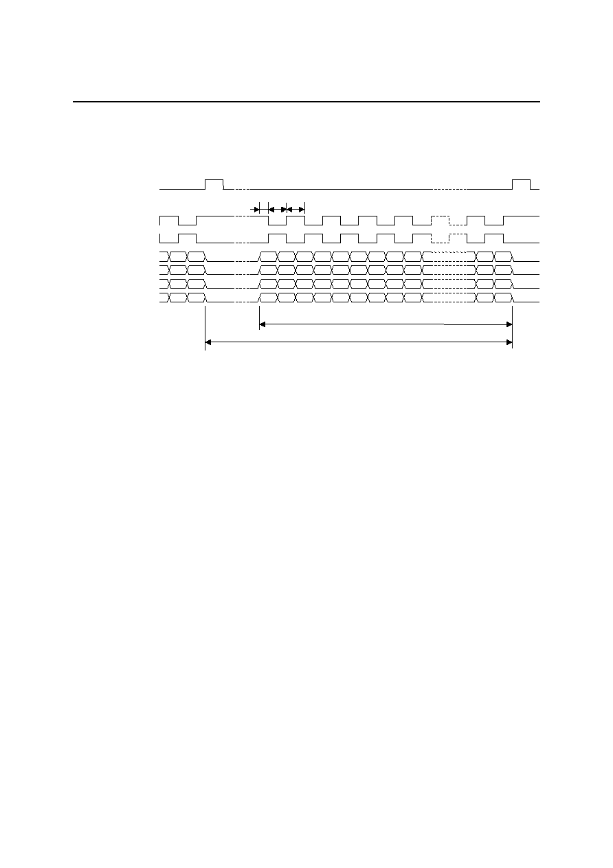
FEDL87V3104-03
OKI Semiconductor
ML87V3104
62/69
1.3 Color STN, 4-bit 2-phase mode
R0
G0
B0
R1
G1
B1
R2
G2
B2
R3
G3
B3
R4
G4
B4
R5
G5
B5
R6
G6
B6
R7
G7
B7
R8
G8
B8
R9
G9
B9
R10 G10
CPS
B10
G11
R12
B12
DDA3
DDA2
DDA1
DDA0
CP
(MSCSZH+1)
�
3/4 [TCP]
(LCPCYC+1) [TCP]
1/2TCP
LCP
G
n-3
B
n-3
R
n-2
G
n-2
B
n-2
R
n-1
G
n-1
B
n-1
TCP TCP
G
n-3
B
n-3
R
n-2
G
n-2
B
n-2
R
n-1
G
n-1
B
n-1
TCP = TX (TX is the XOSCI input clock period)

FEDL87V3104-03
OKI Semiconductor
ML87V3104
63/69
1.4 Monochrome STN, 4-bit mode
DDA3
DDA2
DDA1
DDA0
0
1
2
3
4
5
6
7
8
9
10
11
12
13
14
15
16
17
18
19
20
21
22
23
24
25
26
27
28
29
30
31
32
33
34
35
CP
n-8
n-7
n-6
n-5
n-4
n-3
n-2
n-1
(MSCSZH+1) / 4 [TCP]
(LCPCYC+1) [TCP]
TCP
LCP
n-8
n-7
n-6
n-5
n-4
n-3
n-2
n-1
TCP = 4TX (TX is the XOSCI input clock period)
1.5 Monochrome STN, 8-bit mode
0
1
2
3
4
5
6
7
8
9
10
11
12
13
14
15
16
17
18
19
20
21
22
23
24
25
26
27
28
29
30
31
DDB3
DDB2
DDB1
DDB0
32
33
34
35
36
37
38
39
DDA3
DDA2
DDA1
DDA0
CP
(MSCSZH+1) / 8 [TCP]
(LCPCYC+1) [TCP]
TCP
LCP
n-7
n-6
n-5
n-4
n-3
n-2
n-1
n-8
n-7
n-6
n-5
n-4
n-3
n-2
n-1
n-8
TCP = 8TX (TX is the XOSCI input clock period)

FEDL87V3104-03
OKI Semiconductor
ML87V3104
64/69
1.6 Monochrome STN, 4-bit 2-phase mode
0
1
2
3
4
5
6
7
8
9
10
11
12
13
14
15
16
17
18
19
20
21
22
23
24
25
26
27
28
29
30
31
CPS
32
34
36
38
DDA3
DDA2
DDA1
DDA0
CP
n-8
n-7
n-6
n-5
n-4
n-3
n-2
n-1
(MSCSZH+1) / 4 [TCP]
(LCPCYC+1) [TCP]
1/2TCP
LCP
TCP
n-8
n-7
n-6
n-5
n-4
n-3
n-2
n-1
TCP
TCP = 4TX (TX is the XOSCI input clock period)

FEDL87V3104-03
OKI Semiconductor
ML87V3104
65/69
1.7 Color TFT, 12-bit mode
TCP = TX (TX is the XOSCI input clock period)
1.8 Color TFT, 16-bit mode
TCP = TX (TX is the XOSCI input clock period)
DDA
3 (R3)
DDA2 (R2)
DDA1 (R1)
DDA0 (R0)
DDB
3 (G3)
DDB2 (G2)
DDB1 (G1)
DDB0 (G0)
DDC
3 (B3)
DDC2 (B2)
DDC1 (B1)
DDC0 (B0)
0
1
2
3
4
5
6
7
8
CP
n-2
n-1
(DPSCH+1) [TCP
]
(DCYCH+1) [TCP
]
T
CP
LCP
n-2
n-1
0
1
2
3
4
5
6
7
8
n-2
n-1
n-2
n-1
0
1
2
3
4
5
6
7
8
n-2
n-1
n-2
n-1
0
1
2
3
4
5
6
7
8
n-2
n-1
n-2
n-1
0
1
2
3
4
5
6
7
8
n-2
n-1
n-2
n-1
0
1
2
3
4
5
6
7
8
n-2
n-1
n-2
n-1
0
1
2
3
4
5
6
7
8
n-2
n-1
n-2
n-1
0
1
2
3
4
5
6
7
8
n-2
n-1
n-2
n-1
0
1
2
3
4
5
6
7
8
n-2
n-1
n-2
n-1
0
1
2
3
4
5
6
7
8
n-2
n-1
n-2
n-1
0
1
2
3
4
5
6
7
8
n-2
n-1
n-2
n-1
0
1
2
3
4
5
6
7
8
n-2
n-1
n-2
n-1
CPS
DDA3 (R5)
DDA2 (R4)
DDA1 (R3)
DDA0 (R2)
CP
LCP
DDB3 (R1)
DDB2 (G5)
DDB1 (G4)
DDB0 (G3)
DDC3 (G2)
DDC2 (G1)
DDC1 (G0)
DDC0 (B5)
DDD3 (B4)
DDD2 (B3)
DDD1 (B2)
DDD0 (B1)
0
1
2
3
4
5
6
7
8
n-2
n-1
(DPSCH+1) [TCP]
(DCYCH+1) [TCP]
TCP
n-2
n-1
0
1
2
3
4
5
6
7
8
n-2
n-1
n-2
n-1
0
1
2
3
4
5
6
7
8
n-2
n-1
n-2
n-1
0
1
2
3
4
5
6
7
8
n-2
n-1
n-2
n-1
0
1
2
3
4
5
6
7
8
n-2
n-1
n-2
n-1
0
1
2
3
4
5
6
7
8
n-2
n-1
n-2
n-1
0
1
2
3
4
5
6
7
8
n-2
n-1
n-2
n-1
0
1
2
3
4
5
6
7
8
n-2
n-1
n-2
n-1
0
1
2
3
4
5
6
7
8
n-2
n-1
n-2
n-1
0
1
2
3
4
5
6
7
8
n-2
n-1
n-2
n-1
0
1
2
3
4
5
6
7
8
n-2
n-1
n-2
n-1
0
1
2
3
4
5
6
7
8
n-2
n-1
n-2
n-1
0
1
2
3
4
5
6
7
8
n-2
n-1
n-2
n-1
0
1
2
3
4
5
6
7
8
n-2
n-1
n-2
n-1
0
1
2
3
4
5
6
7
8
n-2
n-1
n-2
n-1
0
1
2
3
4
5
6
7
8
n-2
n-1
n-2
n-1
CPS

FEDL87V3104-03
OKI Semiconductor
ML87V3104
66/69
1.9 STN vertical timing
DDA3-0
DDB3-0
DDC3-0
DDD3-0
LCP
(MSCSZV+1) [TLCP]
(FRPCYC+1) [TLCP]
TLCP
FRP
Line 0
Line 1
Line 2
Line 3
Line 4
Line 0
Line 1
Line 2
Line 3
Line 4
Line 0
Line 1
Line 2
Line 3
Line 4
Line 0
Line 1
Line 2
Line 3
Line 4
(FRPSTA+1) [TLCP]
1.10 TFT vertical timing
DDA3-0
DDB3-0
DDC3-0
DDD3-0
LCP
(MSCSZV+1) [TLCP]
(FRPCYC+1) [TLCP]
TLCP
FRP
Line 0
Line 1
Line 2
Line 3
Line 0
Line 1
Line 2
Line 3
Line 0
Line 1
Line 2
Line 3
Line 0
Line 1
Line 2
Line 3
(FRPSTA + 1) [TLCP]
FRPWID
CPS
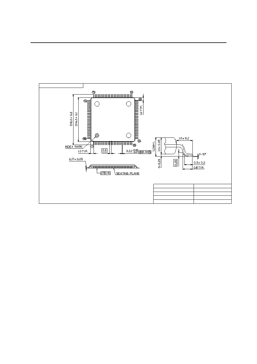
FEDL87V3104-03
OKI Semiconductor
ML87V3104
67/69
PACKAGE DIMENSIONS
TQFP100-P-1414-0.50-K
Mirror finish
Package material
Epoxy resin
Lead frame material
42 alloy
Pin treatment
Solder plating (
5�m)
Package weight (g)
0.55 TYP.
5
Rev. No./Last Revised
4/Oct. 28, 1996
Notes for Mounting the Surface Mount Type Package
The surface mount type packages are very susceptible to heat in reflow mounting and humidity absorbed in storage.
Therefore, before you perform reflow mounting, contact Oki's responsible sales person for the product name,
package name, pin number, package code and desired mounting conditions (reflow method, temperature and
times).
(Unit: mm)

FEDL87V3104-03
OKI Semiconductor
ML87V3104
68/69
REVISION HISTORY
Page
Document
No.
Date
Previous
Edition
Current
Edition
Description
FEDL87V3104-01
Feb., 2001
�
�
First version released
FEDL87V3104-02 Nov.,
2001
67
67
1
1
Fixed the memory size descriptions
4
4
Added the pin types
5, 17
5, 17
Added the notations
10 10
Fixed the behavior at the Portrait mode
19 19
COLORD[1:0] [2:0]
20 20
"352"
"360"
27 27
Added the descriptions
36 36
Added the descriptions of the bit number
40 40
LCDDAT[1:0] [2:0]
42 42
#02h bit3
"--"
"
W/R
"
42 42
IMDBPP[1:0] [2:0]
58, 59
58, 59
Temp. ranges 0 to 70
�
C -45 to 85
�
C
FEDL87V3104-03
Nov. 28, 2003
�
68, 69
Added "REV. HISTORY" and "NOTICE" pages

FEDL87V3104-03
OKI Semiconductor
ML87V3104
69/69
NOTICE
1. The information contained herein can change without notice owing to product and/or technical improvements.
Before using the product, please make sure that the information being referred to is up-to-date.
2. The outline of action and examples for application circuits described herein have been chosen as an explanation
for the standard action and performance of the product. When planning to use the product, please ensure that the
external conditions are reflected in the actual circuit, assembly, and program designs.
3. When designing your product, please use our product below the specified maximum ratings and within the
specified operating ranges including, but not limited to, operating voltage, power dissipation, and operating
temperature.
4. Oki assumes no responsibility or liability whatsoever for any failure or unusual or unexpected operation
resulting from misuse, neglect, improper installation, repair, alteration or accident, improper handling, or
unusual physical or electrical stress including, but not limited to, exposure to parameters beyond the specified
maximum ratings or operation outside the specified operating range.
5. Neither indemnity against nor license of a third party's industrial and intellectual property right, etc. is granted
by us in connection with the use of the product and/or the information and drawings contained herein. No
responsibility is assumed by us for any infringement of a third party's right which may result from the use
thereof.
6. The products listed in this document are intended for use in general electronics equipment for commercial
applications (e.g., office automation, communication equipment, measurement equipment, consumer
electronics, etc.). These products are not, unless specifically authorized by Oki, authorized for use in any
system or application that requires special or enhanced quality and reliability characteristics nor in any system
or application where the failure of such system or application may result in the loss or damage of property, or
death or injury to humans.
Such applications include, but are not limited to, traffic and automotive equipment, safety devices, aerospace
equipment, nuclear power control, medical equipment, and life-support systems.
7. Certain products in this document may need government approval before they can be exported to particular
countries. The purchaser assumes the responsibility of determining the legality of export of these products and
will take appropriate and necessary steps at their own expense for these.
8. No part of the contents contained herein may be reprinted or reproduced without our prior permission.
Copyright 2003 Oki Electric Industry Co., Ltd.