
OKI Semiconductor
PEDL9051G-01
Issue Date: Jul. 23, 2002
ML9051G
Preliminary
132-Channel LCD Driver with Built-in RAM for LCD Dot Matrix Displays
1/74
GENERAL DESCRIPTION
The ML9051G is an LSI for dot matrix graphic LCD devices carrying out bit map display. This LSI can drive a dot
matrix graphic LCD display panel under the control of an 8-bit microcomputer (hereinafter described MPU).
Since all the functions necessary for driving a bit map type LCD device are incorporated in a single chip, using the
ML9051G makes it possible to realize a bit map type dot matrix graphic LCD display system with only a few
chips.
Since the bit map method in which one bit of display RAM data turns ON or OFF one dot in the display panel, it is
possible to carry out displays with a high degree of freedom such as Chinese character displays, etc. With one chip,
it is possible to construct a graphic display system with a maximum of 49
�
132 dots. The display can be expanded
further using two chips. However, the ML9051G is not used in a multiple chip configuration when a line reversal
drive is set.
The ML9051G is made using a CMOS process. Because it has a built-in RAM, low power consumption is one of
its features, and is therefore suitable for displays in battery-operated portable equipment.
The ML9051G has 49 common signal outputs and 132 segment signal outputs and one chip can drive a display of
up to 49
�
132 dots.
FEATURES
�
Direct display of the RAM data using the bit map method
Display RAM data "1" ... Dot is displayed
Display RAM data "0" ... Dot is not displayed (during forward display)
�
Display RAM capacity
65
�
132 = 8580 bits
�
LCD Drive circuits
49 common outputs, 132 segment outputs
�
MPU interface: Can select an 8-bit parallel or serial interface
�
Built-in voltage multiplier circuit for the LCD drive power supply
�
Built-in LCD drive voltage adjustment circuit
�
Built-in LCD drive bias generator circuit
�
Can select frame reversal drive or line reversal drive by command
�
Built-in oscillator circuit (Internal RC oscillator/external clock input)
�
A variety of commands
Read/write of display data, display ON/OFF, forward/reverse display, all dots ON/all dots OFF, set page
address, set display start address, etc.
�
Power supply voltage
Logic power supply: V
DD
-V
SS
= 3.7 V to 5.5 V
Voltage multiplier reference voltage: V
IN
-V
SS
= 3.7 V to 5.5 V
(2- to 4-time multiplier available)
LCD Drive voltage: V
BI
-V
SS
= 6.0 to 18 V
�
Package: Gold bump chip (Bump hardness: Low, DV)
�
This device is not resistant to radiation and light.

PEDL9051G-01
OKI Semiconductor
ML9051G
2/74
BLOCK DIAGRAM
V
DD
V
IN
FRS
V1
V2
V3
V4
V5
V
SS
VS1�
VS2�
VC3+
VC4+
VC5+
VC6+
V
OUT
VR
VRS
IRS
HPM
SEGMENT
Drivers
COMMON
Drivers
Common Output state
selection circuit
Display data latch circuit
Display data RAM
65
�
132
Column address circuit
Bus holder
C86
C
S
1
CS2
A
0
R
D
(E)
WR
(R/
W
)
P/
S
R
ES
DB7(SI)
DB6(SCL)
DB5
DB4
DB3
DB2
DB1
DB0
Oscillator circuit
Display timing generator circuit
COMS
COMS0
COM47
COM0
SEG131
SEG0
Line address circuit
I/O Buf
f
er
Page address circuit
Power supply circuit
Command decoder
Status
MPU lnterface
FR
CL
DOF
M/
S
CLS
COMS1
TEST0
TEST1

PEDL9051G-01
OKI Semiconductor
ML9051G
3/74
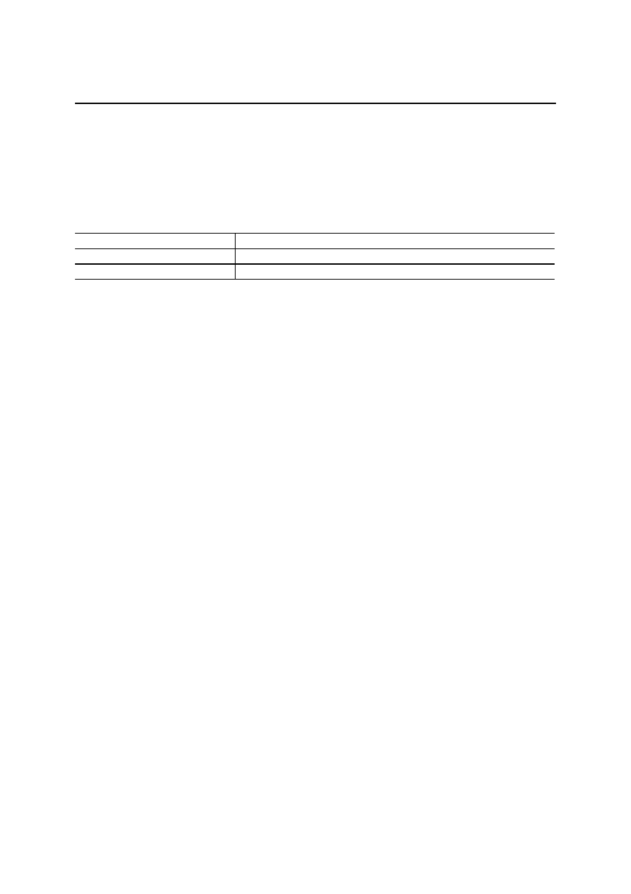
ABSOLUTE MAXIMUM RATINGS
V
SS
= 0 V
Parameter
Symbol
Condition
Rated value
Unit
Applicable pins
Power supply voltage
V
DD
Tj = 25�C
�0.3 to +7
V
V
DD
Bias voltage
V
BI
Tj = 25�C
�0.3 to +20
V
V1 to V5
Voltage multiplier output
voltage
V
OUT
Tj = 25�C
�0.3 to +20
V
V
OUT
Voltage multiplier reference
voltage
V
IN
2-time multiplication
3-time multiplication
4-time multiplication
�0.3 to +5.5
�0.3 to +5.5
�0.3 to +5.0
V V
IN
Input voltage
V
I
Tj = 25�C
�0.3 to V
DD
+0.3 V All
inputs
Storage temperature range
T
STG
Chip
�55 to +125
�C
--
Tj: Chip surface temperature
RECOMMENDED OPERATING CONDITIONS
V
SS
= 0 V
Parameter
Symbol
Condition
Rated value
Unit
Applicable pins
Power supply voltage
V
DD
--
3.7 to 5.5
V
V
DD
Bias voltage
V
BI
--
6 to 18
V
V1 to V5
Voltage multiplier reference
voltage
V
IN
2-time multiplication
3-time multiplication
4-time multiplication
3.7 to 5.5
3.7 to 5.5
3.7 to 4.5
V V
IN
Voltage multiplier output
voltage
V
OUT
External input
6.0 to 18
V
V
OUT
Operating temperature range
T
JOP
--
�40 to +85
�C
--
Note 1: The electrical characteristics are influenced by COG trace resistance. This LSI always has to
be evaluated before using.
Note 2: The voltages V
DD
, V1 to V5, and V
OUT
are values taking V
SS
= 0 V as the reference.
Note 3: The highest bias potential is V1 and the lowest is V
SS
.
Note 4: Always maintain the relationship V1
V2
V3
V4
V5
V
SS
among these voltages.
V
CC
GND
V
IN
V
DD
V
SS
V
OUT
V1 to V5
ML9051G
System (MPU)

PEDL9051G-01
OKI Semiconductor
ML9051G
4/74
Note 5: When using an external power supply, follow the procedure for power application.
When applying external power to the V
OUT
pin only, apply V
OUT
after V
DD.
When applying external power to the V1 pin only, apply V1 after V
DD
.
When applying external power to the V1 pin to V5 pin, apply V1 to V5 after V
DD
.
Note that the above (Note 4) must be satisfied including transient state at power application.
Note 6: When using an external power supply, follow the procedure for power removal described
below.
When external power is in use for the V
OUT
pin only, remove V
OUT
after V
DD
.
When external power is in use for the V1 pin only, remove V1 after V
DD
.
When external power is in use for the V1 pin to V5 pin, remove V1 to V5 after V
DD
.
Note that the above (Note 4) must be satisfied including transient state at power removal.

PEDL9051G-01
OKI Semiconductor
ML9051G
5/74
ELECTRICAL CHARACTERISTICS
DC Characteristics
[V
SS
= 0 V, V
DD
= 3.7 to 5.5 V, Tj =�40 to +85�C]
Parameter Symbol
Condition Min
Typ
Max
Unit
Applicable
pins
"H" Input voltage
V
IH
0.8
�
V
DD
-- V
DD
"L" Input voltage
V
IL
0
--
0.2
�
V
DD
V *1
"H" Input voltage
V
IH
0.8
�
V
DD
-- V
DD
"L" Input voltage
V
IL
0
--
0.2
�
V
DD
Hysteresis width
V V
DD
= 5.0 V
--
1.0
--
V *2
"H" output voltage
V
OH
I
OH
= �0.5 mA
0.8
�
V
DD
--
--
"L" output voltage
V
OL
I
OL
= 0.5 mA
--
--
0.2
�
V
DD
V *3
"H" Input current
I
IH
V
I
= V
DD
�1.0
--
+1.0
"L" Input current
I
IL
V
I
= 0 V
�3.0
--
+3.0
�
A *4
*5
V1 output voltage
temperature gradient
V1TC
Tj = 25�C
V1 = 12 V
-- �0.05 -- %/�C V1
V1 output voltage
V1
*6 10.63
10.85
11.07
V
V1
3-time
multiplication *7
13.0 -- -- V V
OUT
Voltage multiplier
output voltage
V
OUT
4-time
multiplication *8
15.9 -- -- V V
OUT
V
OUT
- V1 voltage
Vot1
*9
0.6
--
--
V
V
OUT,
V1
LCD driver ON
resistance
R
ON
I
O
= �50 �A
--
--
10
k
SEG1 to 131,
COMS0,
COMS1,
COM0 to 47
27 33 39 kHz *10
Internal
oscillation
f
OSC
Tj = 25�C
21 -- 47
kHz
Oscillator
frequency External
input
f
EXT
14
17
20
kHz
CL*10
*1:
A0, DB0 to DB5, DB7 (SI),
CS1
, CS2, CLS, FR, M/
S
, C86, P/
S
,
DOF
, IRS,
HPM
Pins
*2:
RD
(E),
WR
(R/
W
),
RES
, CL, DB6 (SCL) Pins
*3:
DB0 to DB7, FR, FRS,
DOF
, CL Pins
*4: A0,
RD
(E),
WR
(R/
W
),
CS1
, CS2, CLS, M/
S
, C86, P/
S
,
RES
, IRS,
HPM
Pins
*5:
Applicable to the pins DB0 to DB5, DB6 (SCL), DB7 (SI), CL, FR,
DOF
in the high impedance
state.
*6:
Tj = 25�C,
= 31, (1+Rb/Ra) = 4, V
OUT
= 13.5 V (External input), LCD drive output = no-load
*7:
During high-power mode, V
IN
= 4.8 V, voltage multiplier capacitor C1 = 3.7 to 5.7
�
F, voltage
multiplier output load current I = 500
�
A. Only a voltage multiplier circuit operates, not activating
the voltage adjustment circuit and V/F circuit, by command "2C".
*8:
During high-power mode, V
IN
= 4.5 V, voltage multiplier capacitor C1 = 3.7 to 5.7
�
F, voltage
multiplier output load current I = 500
�
A. Only a voltage multiplier circuit operates, not activating
the voltage adjustment circuit and V/F circuit, by command "2C".

PEDL9051G-01
OKI Semiconductor
ML9051G
6/74
*9:
During high-power mode, V1 load current I = 400
�
A. 8 V is externally input to V
OUT.
The voltage adjustment circuit and V/F circuit operate by command "2B". LCD output = no load
*10: See Table 1 for the relationship between the oscillator frequency and the frame frequency.
Table 1. Relationship among the oscillator frequency (f
OSC
), display clock frequency (f
LCDCK
), and
LCD frame frequency (f
FR
)
Parameter
Display clock frequency
(f
LCDCK
)
LCD frame frequency
(f
FR
)
When the internal oscillator is used
f
OSC
/8 f
OSC
/(8
�
49)
ML9051G
When the internal oscillator is not used
External input (f
LCDCK
) f
LCDCK
/196

PEDL9051G-01
OKI Semiconductor
ML9051G
7/74
�
Operating current consumption value
(1) During display operation, internal power supply OFF (The current flowing through V
DD
with V1 to V5
externally applied when an external power supply is used, not including the current for the LCD drive)
[V
SS
= 0 V, Tj = 25�C]
Rated value
Display mode
Symbol
Condition
Min Typ Max
Unit
V
DD
= 5 V, V1- V
SS
= 11 V, no load
--
25
50
All-white I
DD
V
DD
= 3.7 V, V1- V
SS
= 8 V, no load
--
15
35
�
A
V
DD
= 5 V, V1- V
SS
= 11 V, no load
--
25
50
Checker pattern
I
DD
V
DD
= 3.7 V, V1- V
SS
= 8 V, no load
--
15
35
�
A
(2) During display operation, internal power supply ON (Total of currents flowing through V
DD
and V
IN
)
[V
SS
= 0 V, Tj = 25�C]
Rated value
Display
mode
Symbol Condition
Min Typ Max
Unit
Normal mode
--
225
330
Frame reversal,
V
DD,
V
IN
= 5 V, 3-time
voltage multiplication
V1 - V
SS
= 11 V, no load
High-power mode
--
515
790
Normal mode
--
255
360
Frame reversal,
V
DD,
V
IN
= 3.7 V, 4-time
voltage multiplication
V1 - V
SS
= 8 V, no load
High-power mode
--
605
890
All-white I
DDIN
16-line reversal,
V
DD,
V
IN
= 5 V, 3-time
voltage multiplication
V1 - V
SS
= 11 V, no load
High-power mode
--
525
810
�
A
Normal mode
--
295
430
Frame reversal,
V
DD,
V
IN
= 5 V, 3-time
voltage multiplication
V1 - V
SS
= 11 V, no load
High-power mode
--
585
860
Normal mode
--
325
515
Frame reversal,
V
DD,
V
IN
= 3.7 V, 4-time
voltage multiplication
V1 - V
SS
= 8 V, no load
High-power mode
--
675 1030
Checker
pattern
I
DDIN
16-line reversal,
V
DD,
V
IN
= 5 V, 3-time
voltage multiplication
V1 - V
SS
= 11 V, no load
High-power mode
--
595
875
�
A
�
Power save mode current consumption
[V
SS
= 0 V, Tj = 25�C]
Rated value
Parameter Symbol
Condition
Min Typ Max
Unit
Sleep mode
I
DDS1
V
DD
= 3.7 V
--
0.3
5
Standby mode
I
DDS2
V
DD
= 3.7 V
--
7
15
�
A

PEDL9051G-01
OKI Semiconductor
ML9051G
8/74
Parallel Interface Timing Characteristics
�
System bus Write characteristics 1 (80-series MPU)
�
System bus Read characteristics 1 (80-series MPU)
A0
CS1
(CS2 = "H")
WR
DB0 to DB7
(Write)
t
AW8
t
DS8
t
DH8
t
CCLW
t
CCHW
t
AH8
t
CYC8
V
IL
V
IH
V
IL
V
IH
V
IH
V
IL
V
IH
V
IL
V
IH
V
IL
V
IH
V
IL
V
IH
A0
CS1
(CS2 = "H")
RD
DB0 to DB7
(Read)
t
AW8
t
ACC8
t
CCLR
t
CCHR
t
AH8
t
OH8
t
CYC8
V
IL
V
IH
V
IL
V
IH
V
IL
V
IH
V
IL
V
IH
V
IH
V
OH
V
OH
V
OL
V
OL

PEDL9051G-01
OKI Semiconductor
ML9051G
9/74
[V
DD
= 4.5 to 5.5 V, Tj = �40 to +85�C]
Rated value
Parameter Symbol
Condition
Min Max
Unit
Address hold time
t
AH8
5
--
Address setup time
t
AW8
5
--
System cycle time
t
CYC8
166
--
Control L pulse width (
WR
) t
CCLW
30
--
Control L pulse width (
RD
)
t
CCLR
70
--
Control H pulse width (
WR
)
t
CCHW
55
--
Control H pulse width (
RD
) t
CCHR
55
--
Data setup time
t
DS8
30
--
Data hold time
t
DH8
10
--
RD
Access time
t
ACC8
--
70
Output disable time
t
OH8
CL = 100 pF
5 50
ns
[V
DD
= 3.7 to 4.5 V, Tj = �40 to +85�C]
Rated value
Parameter Symbol
Condition
Min Max
Unit
Address hold time
t
AH8
5
--
Address setup time
t
AW8
5
--
System cycle time
t
CYC8
300
--
Control L pulse width (
WR
) t
CCLW
60
--
Control L pulse width (
RD
)
t
CCLR
120
--
Control H pulse width (
WR
)
t
CCHW
60
--
Control H pulse width (
RD
) t
CCHR
60
--
Data setup time
t
DS8
40
--
Data hold time
t
DH8
15
--
RD
Access time
t
ACC8
--
140
Output disable time
t
OH8
CL = 100 pF
10 100
ns
Note 1: The input signal rise and fall times are specified as 15ns or less.
When using the system cycle time for fast speed, the specified values are (tr + tf)
(t
CYC8
�
t
CCLW
� t
CCHW
) or (tr + tf)
(t
CYC8
� t
CCLR
� t
CCHR
).
Note 2: All timings are specified taking the levels of 20% and 80% of V
DD
as the reference.
Note 3: The values of t
CCLW
and t
CCLR
are specified during the overlapping period of
CS1
at "L" (CS2 =
"H") and the "L" levels of
WR
and
RD
, respectively.

PEDL9051G-01
OKI Semiconductor
ML9051G
10/74
�
System bus Write characteristics 2 (68-series MPU)
�
System bus Read characteristics 2 (68-series MPU)
A0
CS1
(CS2 = "H")
E
R/
W
DB0 to DB7
(Write)
t
AW6
t
DS6
t
DH6
t
EWHW
t
EWLW
t
AH6
t
CYC6
V
IH
V
IL
V
IL
V
IL
V
IH
V
IL
V
IL
V
IL
V
IH
V
IH
V
IL
V
IH
V
IL
V
IH
V
IL
A0
CS1
(CS2 = "H")
E
DB0 to DB7
(Read)
t
AW6
t
ACC6
t
EWHR
t
EWLR
t
AH6
t
OH6
t
CYC6
R/
W
V
IL
V
IL
V
IH
V
IH
V
IL
V
IH
V
IL
V
IH
V
IL
V
IH
V
IH
V
OH
V
OL
V
OH
V
OL

PEDL9051G-01
OKI Semiconductor
ML9051G
11/74
[V
DD
= 4.5 to 5.5 V, Tj = �40 to +85�C]
Rated value
Parameter Symbol
Condition
Min Max
Unit
Address hold time
t
AH6
5
--
Address setup time
t
AW6
5
--
System cycle time
t
CYC6
166
--
Data setup time
t
DS6
30
--
Data hold time
t
DH6
10
--
Access time
t
ACC6
CL = 100 pF
--
70
Output disable time
t
OH6
10
50
Read t
EWHR
70
--
Enable H pulse width
Write t
EWHW
30
--
Read t
EWLR
60
--
Enable L pulse width
Write t
EWLW
60
--
ns
[V
DD
= 3.7 to 4.5 V, Tj = �40 to +85�C]
Rated value
Parameter Symbol
Condition
Min Max
Unit
Address hold time
t
AH6
5
--
Address setup time
t
AW6
5
--
System cycle time
t
CYC6
300
--
Data setup time
t
DS6
40
--
Data hold time
t
DH6
15
--
Access time
t
ACC6
-- 140
Output disable time
t
OH6
CL = 100 pF
10 100
Read t
EWHR
120
--
Enable H pulse width
Write t
EWHW
60
--
Read t
EWLR
60
--
Enable L pulse width
Write t
EWLW
60
--
ns
Note 1: The input signal rise and fall times are specified as 15ns or less.
When using the system cycle time for fast speed, the specified values are (tr + tf)
(t
CYC6
�
t
EWLW
� t
EWHW
) or (tr + tf)
(t
CYC6
� t
EWLR
� t
EWHR
).
Note 2: All timings are specified taking the levels of 20% and 80% of V
DD
as the reference.
Note 3: The values of t
EWLW
and t
EWLR
are specified during the overlapping period of
CS1
at "L" (CS2 =
"H") and the "H" level of E.

PEDL9051G-01
OKI Semiconductor
ML9051G
12/74
Serial Interface Timing Characteristics
�
Serial interface
[V
DD
= 4.5 to 5.5 V, Tj = �40 to +85�C]
Rated value
Parameter Symbol
Condition
Min Max
Unit
Serial clock period
t
SCYC
200
--
SCL "H" Pulse width
t
SHW
75
--
SCL "L" Pulse width
t
SLW
75
--
Adress setup time
t
SAS
50
--
Address hold time
t
SAH
100
--
Data setup time
t
SDS
50
--
Data hold time
t
SDH
50
--
CS setup time
t
CSS
100
--
CS hold time
t
CSH
100
--
ns
Note 1: The input signal rise and fall times are specified as 15ns or less.
Note 2: All timings are specified taking the levels of 20% and 80% of V
DD
as the reference.
CS1
(CS2 = "1")
SCL
SI
A0
t
CSS
t
SLW
t
SDS
t
SHW
t
CSH
t
SAS
t
SCYC
t
SAH
t
SDH
t
f
t
r
V
IL
V
IH
V
IL
V
IL
V
IL
V
IH
V
IL
V
IH
V
IL
V
IH
V
IL
V
IH
V
IL
V
IH
V
IL
V
IH

PEDL9051G-01
OKI Semiconductor
ML9051G
13/74
[V
DD
= 3.7 to 4.5 V, Tj = �40 to +85�C]
Rated value
Parameter Symbol
Condition
Min Max
Unit
Serial clock period
t
SCYC
250
--
SCL "H" Pulse width
t
SHW
100
--
SCL "L" Pulse width
t
SLW
100
--
Address setup time
t
SAS
150
--
Address hold time
t
SAH
150
--
Data setup time
t
SDS
100
--
Data hold time
t
SDH
100
--
CS setup time
t
CSS
150
--
CS hold time
t
CSH
150
--
ns
Note 1: The input signal rise and fall times are specified as 15ns or less.
Note 2: All timings are specified taking the levels of 20% and 80% of V
DD
as the reference.
�
Display control output timing
CL(OUT)
FR
t
DFR
V
OH
V
IH
V
IL
[V
DD
= 4.5 to 5.5 V, Tj = �40 to +85�C]
Rated value
Parameter Symbol
Condition
Min Typ Max
Unit
FR Delay time
t
DFR
CL = 50 pF
--
10
40
ns
[V
DD
= 3.7 to 4.5 V, Tj = �40 to +85�C]
Rated value
Parameter Symbol
Condition
Min Typ Max
Unit
FR Delay time
t
DFR
CL = 50 pF
--
20
80
ns
Note 1: All timings are specified taking the levels of 20% and 80% of V
DD
as the reference.
Note 2: Valid only when the device operates in master mode.

PEDL9051G-01
OKI Semiconductor
ML9051G
14/74
�
Reset input timing
[V
DD
= 4.5 to 5.5 V, Tj = �40 to +85�C]
Rated value
Parameter Symbol
Condition
Min Typ Max
Unit
Reset time
t
R
--
--
0.5
Reset "L" pulse width
t
RW
0.5 -- --
�s
[V
DD
= 3.7 to 4.5 V, Tj = �40 to +85�C]
Rated value
Parameter Symbol
Condition
Min Typ Max
Unit
Reset time
t
R
--
--
1
Reset "L" pulse width
t
RW
1 -- --
�s
Note 1: The input signal rise and fall times (t
r
, t
f
) are specified as 15 ns or less.
Note 2: All timings are specified taking the levels of 20% and 80% of V
DD
as the reference.
RES
Internal
state
Being
reset
Reset
complete
t
RW
t
R
t
f
t
r
V
IH
V
IL
V
IL
V
IH

PEDL9051G-01
OKI Semiconductor
ML9051G
15/74
PIN DESCRIPTION
Function Pin
name
Number
of pins
I/O Description
DB0 to
DB7
8 I/O
These are 8-bit bi-directional data bus pins that can be connected to
8-bit standard MPU data bus pins. When a serial interface is selected
(P/
S
= "L"):
DB7: Serial data input pin (SI)
DB6: Serial clock input pin (SCL)
In this case, DB0 to DB5 will be in the high impedance state. DB0 to
DB7 will all be in the high impedance state when the chip select is in
the inactive state.
Fix the DB0 to DB5 pins at "H" or "L" level.
A0 1
I
Normally, the lowest bit of the MPU address bus is connected and
used for distinguishing between data and commands.
A0 = "H": Indicates that DB0 to DB7 is display data.
A1 = "L": Indicates that DB0 to DB7 is control data.
RES
1 I
Initial setting is made by making
RES
= "L". The reset operation is
made during the active level of the
RES
signal.
CS1
CS2
2 I
These are the chip select signals. The Chip Select of the LSI
becomes active when
CS1
is "L" and also CS2 is "H" and allows the
input/output of data or commands.
RD
(E)
1 I
The active level of this signal is "L" when connected to an 80-series
MPU. This pin is connected to the
RD
signal of the 80-series MPU,
and the data bus of the ML9051G goes into the output state when this
signal is "L".
The active level of this signal is "H" when connected to a 68-series
MPU. This pin will be the Enable and clock input pin when connected
to a 68-series MPU.
When a serial interface is selected (P/
S
= "L"), fix this pin at "H" or "L"
level.
WR
(R/
W
)
1 I
The active level of this signal is "L" when connected to an 80-series
MPU. This pin is connected to the
WR
signal of the 80-series MPU.
The data on the data bus is latched into the ML9051G at the rising
edge of the
WR
signal.
When connected to a 68-series MPU, this pin becomes the input pin
for the Read/Write control signal.
R/
W
= "H": Read, R/
W
= "L": Write
When a serial interface is selected (P/
S
= "L"), fix this pin at "H" or "L"
level.
MPU
Interface
C86 1 I
This is the pin for selecting the MPU interface type.
C86 = "H": 68-Series MPU interface.
C86 = "L": 80-Series MPU interface.

PEDL9051G-01
OKI Semiconductor
ML9051G
16/74
Function Pin
name
Number
of pins
I/O Description
This is the pin for selecting parallel data input or serial data input.
P/
S
= "H": Parallel data input.
P/
S
= "L": Serial data input.
The pins of the LSI have the following functions depending on the
state of P/
S
input.
P/
S
Data/command
Data Read/Write
Serial clock
"H"
A0
DB0 to DB7
RD
,
WR
--
"L" A0
SI
(D7)
--
SCL(DB6)
MPU
Interface
P/
S
1
I
During serial data input, it is not possible to read the display data in
the RAM
Oscillator
circuit
CLS 1 I
This is the pin for selecting whether to enable or disable the internal
oscillator circuit for the display clock.
CLS = "H": The internal oscillator circuit is enabled.
CLS = "L": The internal oscillator circuit is disabled (External input).
When CLS = "L", the display clock is input at the pin CL.
This is the pin for selecting whether master operation or slave
operation is made towards the ML9051G. During master operation,
the synchronization with the LCD display system is achieved by
inputting the timing signals necessary for LCD display.
M/
S
= "H": Master operation
M/
S
= "L": Slave operation
The functions of the different circuits and pins will be as follows
depending on the states of M/
S
and CLS signals.
M/
S
CLS
Oscillator
circuit
Power
supply circuit
CL FR FRS
DOF
"H" Enabled Enabled Output Output Output Output
"H"
"L" Disabled Enabled Input Output Output Output
"H" Disabled Disabled Input
Input Output Input
"L"
"L" Disabled Disabled Input Input Output Input
Display
timing
generator
circuit
M/
S
1 I

PEDL9051G-01
OKI Semiconductor
ML9051G
17/74
Function Pin
name
Number
of pins
I/O Description
This is the display clock input/output pin.
The function of this pin will be as follows depending on the states of
M/
S
and CLS signals.
M/
S
CLS CL
"H" Output
"H"
"L" Input
"H" Input
"L"
"L" Input
CL 1
I/O
When the ML9051G is used in the master/slave mode, the
corresponding CL pin has to be connected.
FR 1
I/O
This is the input/output pin for LCD display frame reversal signal.
M/
S
= "H": Output
M/
S
= "L": Input
When the ML9051G is used in the master/slave mode, the
corresponding FR pin has to be connected.
DOF
1
I/O
This is the blanking control pin for the LCD display.
M/
S
= "H": Output
M/
S
= "L": Input
When the ML9051G is used in the master/slave mode, the
corresponding
DOF
pin has to be connected.
Display
timing
generator
circuit
FRS 1
O
This is the output pin for static drive.
This pin is used in combination with the FR pin.
IRS 1 I
This is the pin for selecting the resistor for adjusting the voltage V1.
IRS = "H": The internal resistor is used.
IRS = "L": The internal resistor is not used. The voltage V1 is
adjusted using the external potential divider resistors connected to
the pins VR. This pin is effective only in the master operation. This
pin is tied to the "H" or the "L" level during slave operation.
HPM
1 I
This is the power control pin for the LCD drive power supply circuit.
HPM
= "H": Normal mode
HPM
= "L": High power mode
This pin is effective only during master operation mode. This pin is
tied to the "H" or the "L" level during slave operation.
V
DD
13
--
These pins are tied to the MPU power supply pin V
CC
.
V
SS
9
--
These are the 0 V pins connected to the system ground (GND).
Power
supply
circuit
V
IN
4
--
These are the reference power supply pins of the voltage multiplier
circuit for driving the LCD.

PEDL9051G-01
OKI Semiconductor
ML9051G
18/74
Function Pin
name
Number
of pins
I/O Description
V
RS
2
--
These are the test pins for the LCD power supply voltage adjustment
circuit. Leave these pins open.
V
OUT
2
I/O
These are the output pins during voltage multiplication. Connect a
capacitor between these pins and V
SS
.
These are the multiple level power supply pins for the LCD power
supply. The voltages specified for the LCD cells are applied to these
pins after resistor network voltage division or after impedance
transformation using operational amplifiers. The voltages are
specified taking V
SS
as the reference, and the following relationship
should be maintained among them.
V1
V2
V3
V4
V5
V
SS
Master operation: When the power supply is ON, the following
voltages are applied to V2 to V5 from the built-in power supply circuit.
The selection of voltages is determined by the LCD bias set
command.
ML9050E
V2 7/8
�
V1
5/6
�
V1
V3 6/8
�
V1
4/6
�
V1
V4 2/8
�
V1
2/6
�
V1
V5 1/8
�
V1
1/6
�
V1
V1
V2
V3
V4
V5
10 I/O
VR 2
I
Voltage adjustment pins. Voltages between V1 and V
SS
are applied
using a resistance voltage divider.
These pins are effective only when the internal resistors for voltage
V1 adjustment are not used (IRS = "L").
Do not use these pins when the internal resistors for voltage V1
adjustment are used (IRS = "H").
VS1� 2 O
These are the pins for connecting the negative side of the capacitors
for voltage multiplication.
Connect capacitors between these pins and VC3+, VC5+.
VS2� 2 O
These are the pins for connecting the negative side of the capacitors
for voltage multiplication.
Connect capacitors between these pins and VC4+, VC6+.
VC3+ 2 O
These are the pins for connecting the positive side of the capacitors
for voltage multiplication.
Connect capacitors between VS1� and these pins.
Power
supply
circuit
VC4+ 2 O
These are the pins for connecting the positive side of the capacitors
for voltage multiplication.
Connect capacitors between VS2� and these pins.

PEDL9051G-01
OKI Semiconductor
ML9051G
19/74
Function Pin
name
Number
of pins
I/O Description
VC5+ 2 O
These are the pins for connecting the positive side of the capacitors
for voltage multiplication.
Connect capacitors between VS1� and these pins.
Power
supply
circuit
VC6+ 2 O
These are the pins for connecting the positive side of the capacitors
for voltage multiplication.
Connect capacitors between VS2� and these pins.
These are the LCD segment drive outputs.
One of the levels among V1, V3, V4, and V
SS
is selected depending
on the combination of the display RAM content and the FR signal
Output voltage
RAM Data
FR
Forward display Reverse display
H H V1 V3
H L V
SS
V4
L H V3
V1
L L V4
V
SS
Power save
--
V
SS
SEG0 to
SEG131
132 O
The output voltage is V
SS
when the Display OFF command is
executed.
These are the LCD common drive outputs.
One of the levels among V1, V2, V5, and V
SS
is selected depending
on the combination of the scan data and the FR signal.
Scan data
FR
Output voltage
H H
V
SS
H L
V1
L H
V2
L L
V5
Power save
--
V
SS
LCD
Drive
output
COM0 to
COM47
48 O
The output voltage is V
SS
when the Display OFF command is
executed.
COMS0
COMS1
2 O
These are the common output pins only for indicators. Both pins
output the same signal. Leave these pins open when they are not
used. The same signal is output in both master and slave operation
modes.
TEST0 1 I
Test pin
TEST1 1 O
These are the pins for testing the IC chip. Leave these pins open
during normal use.
--
DUMMY
72
--
Leave this pin open.

PEDL9051G-01
OKI Semiconductor
ML9051G
20/74
FUNCTIONAL DESCRIPTION
MPU Interface
MPU
Read mode
Write mode
80-Series Pin
RD
= "L"
Pin
WR
= "L"
Pin R/
W
= "H"
Pin R/
W
= "L"
68-Series
Pin E = "H"
Pin E = "H"
In the case of the 80-series MPU interface, a command is started by applying a low pulse to the
RD pin or the WR
pin.
In the case of the 68-series MPU interface, a command is started by applying a high pulse to the E pin.
�
Selection of interface type
The ML9051G carries out data transfer using either the 8-bit bi-directional data bus (DB0 to DB7) or the serial
data input line (SI). Either the 8-bit parallel data input or serial data input can be selected as shown in Table 2 by
setting the P/
S pin to the "H" or the "L" level.
Table 2 Selection of interface type (parallel/serial)
P/
S
CS1
CS2 A0
RD WR
C86
D7
D6
DB0 to DB5
H: Parallel input
L: Serial input
CS1
CS1
CS2
CS2
A0
A0
RD
--
WR
--
C86
--
D7
SI
D6
SCL
DB0 to DB5
--
A hyphen (--) indicates that the pin can be tied to the "H" or the "L" level.
�
Parallel interface
When the parallel interface is selected, (P/
S = "H"), it is possible to connect this LSI directly to the MPU bus of
either an 80-series MPU or a 68-series MPU as shown in Table 3. depending on whether the pin C86 is set to "H"
or "L".
Table 3 Selection of MPU during parallel interface (80�/68�series)
C86
CS1
CS2 A0
RD WR
DB0 to DB7
H: 68-Series MPU bus
L: 80-Series MPU bus
CS1
CS1
CS2
CS2
A0
A0
E
RD
R/
W
WR
DB0 to DB7
DB0 to DB7
The data bus signals are identified as shown in Table 4 below depending on the combination of the signals A0,
RD
(E), and
WR (R/W) of Table 3.
Table 4 Identification of data bus signals during parallel interface
Common 68-Series
80-Series
A0 R/
W RD WR
Display data read
Display data write
Status read
Control data write (command)
1
1
0
0
1
0
1
0
0
1
0
1
1
0
1
0

PEDL9051G-01
OKI Semiconductor
ML9051G
21/74
Serial Interface
When the serial interface is selected (P/
S = "L"), the serial data input (SI) and the serial clock input (SCL) can be
accepted if the chip is in the active state (
CS1 = "L" and CS2 = "H"). The serial interface consists of an 8-bit shift
register and a 3-bit counter. The serial data is read in from the serial data input pin in the sequence DB7, DB6, ... ,
DB0 at the rising edge of the serial clock input, and is converted into parallel data at the rising edge of the 8th serial
clock pulse and processed further. The identification of whether the serial data is display data or command is
judged based on the A0 input, and the data is treated as display data when A0 is "H" and as command when A0 is
"L". The A0 input is read in and identified at the rising edge of the (8
�
n) th serial clock pulse after the chip has
become active. Fig. 1 shows the signal chart of the serial interface. (When the chip is not active, the shift register
and the counter are reset to their initial states. No data read out is possible in the case of the serial interface. It is
necessary to take sufficient care about wiring termination reflection and external noise in the case of the SCL
signal. We recommend verification of operation in an actual unit.)
Fig. 1 Signal chart during serial interface
�
Chip select
The ML9051G has the two chip select pins
CS1 and CS2, and the MPU interface or the serial interface is enabled
only when
CS1 = "L" and CS2 = "H". When the chip select signals are in the inactive state, the DB0 to DB7 lines
will be in the high impedance state and the inputs A0,
RD, and WR will not be effective. When the serial interface
has been selected, the shift register and the counter are reset when the chip select signals are in the inactive state.
�
Accessing the display data RAM and the internal registers
Accessing the ML9051G from the MPU side requires merely that the cycle time (t
CYC
) be satisfied, and high speed
data transfer without requiring any wait time is possible. Also, during the data transfer with the MPU, the
ML9051G carries out a type of pipeline processing between LSIs via a bus holder associated with the internal data
bus. For example, when the MPU writes data in the display data RAM, the data is temporarily stored in the bus
holder, and is then written into the display data RAM before the next data read cycle. Further, when the MPU
reads out data in the display data RAM, first a dummy data read cycle is carried out to temporarily store the data in
the bus holder which is then placed on the system bus and is read out during the next read cycle. There is a
restriction on the read sequence of the display data RAM, which is that the read instruction immediately after
setting the address does not read out the data of that address, but that data is output as the data of the address
specified during the second data read sequence, and hence care should be taken about this during reading.
Therefore, always one dummy read is necessary immediately after setting the address or after a write cycle: (The
status read cannot use dummy read cycles.) This relationship is shown in Figs 2(a) and 2(b).
DB7
SI
SCL
A0
CS2
CS1
1
DB6
2
DB5
3
DB4
4
DB3
5
DB2
6
DB1
7
DB0
8
DB7
9
DB6
10
DB5
11
DB4
12
DB3
13
DB2
14

PEDL9051G-01
OKI Semiconductor
ML9051G
22/74
�
Data write
Fig. 2(a) Write sequence of display data RAM
�
Data read
Fig. 2(b) Read sequence of display data RAM
Dn = Data
N = Address data
�
Busy flag
The busy flag being "1" indicates that the ML9051G is carrying out reset operations, and hence no instruction
other than a status read instruction is accepted during this period. The busy flag is output at pin DB7 when a status
read instruction is executed.
DATA
BUS Holder
Dn
Latch
Dn + 1
WR
MPU
Write Signal
Internal timing
Dn + 2
Dn + 3
Dn
Dn + 1
Dn + 2
Dn + 3
DATA
Column
Address
Read Signal
Address
Preset
N
unknown
Dn
Dn + 1
Preset N
unknown
Dn
Dn + 1
Dn + 2
Increment N + 1
N + 2
RD
MPU
WR
BUS Holder
Internal timing
Address Set
N
Data Read
(Dummy)
Data Read
Dn
Data Read
Dn + 1

PEDL9051G-01
OKI Semiconductor
ML9051G
23/74
Display Data RAM
�
Display data RAM
This is the RAM storing the dot data for display and has an organization of 65 (8 pages
�
8 bits +1)
�
132 bits. It
is possible to access any required bit by specifying the page address and the column address. Since the display data
DB7 to DB0 from the MPU corresponds to the LCD display in the direction of the common lines as shown in Fig.
3, there are fewer restrictions during display data transfer when the ML9051G is used in a multiple chip
configuration, thereby making it easily possible to realize a display with a high degree of freedom. Also, since the
display data RAM read/write from the MPU side is carried out via an I/O buffer, it is done independent of the
signal read operation for the LCD drive. Consequently, the display is not affected by flickering, etc., even when
the display data RAM is accessed asynchronously during the LCD display operation.
DB0
0 1 1 1
...
0
COM0
...
DB1
1 0 0 0
...
0
COM1
...
DB2
0 0 0 0
...
0
COM2
...
DB3
0 1 1 1
...
0
COM3
...
DB4
1 0 0 0
...
0
COM4
...
Display data RAM
LCD Display
Fig. 3 Relationship between display data RAM and LCD display
�
Page address circuit
The page address of the display data RAM is specified using the page address set command as shown in Fig. 4.
Specify the page address again when accessing after changing the page. The page address 8 (DB3, DB2, DB1,
DB0
1, 0, 0, 0) is the RAM area dedicated to the indicator, and only the display data DB0 is valid in this page.
�
Column address circuit
The column address of the display data RAM is specified using the column address set command as shown in Fig.
4. Since the specified column address is incremented (by +1) every time a display data read/write command is
issued, the MPU can access the display data continuously. Further, the incrementing of the column address is
stopped at the column address of 83(H). Since the column address and the page address are independent of each
other, it is necessary, for example, to specify separately the new page address and the new column address when
changing from column 83(H) of page 0 to column 00(H) of page 1. Also, as is shown in Table 5, it is possible to
reverse the correspondence relationship between the display data RAM column address and the segment output
using the ADC command (the segment driver direction select command). This reduces the IC placement
restrictions at the time of assembling LCD modules.
Table 5 Correspondence relationship between the display data RAM column address
and the segment output
SEGMENT Output
ADC
SEG0
SEG131
DB0 = "0"
0(H)
Column Address
83(H)
DB0 = "1"
83(H)
Column Address
0(H)

PEDL9051G-01
OKI Semiconductor
ML9051G
24/74
�
Line address circuit
The line address circuit is used for specifying the line address corresponding to the common output when
displaying the contents of the display data RAM as is shown in Fig. 4. Normally, the topmost line in the display is
specified using the display start line address set command (COM0 output in the forward display state of the
common output, and COM47 output in the reverse display state). The display area is 48 lines in the direction of
increasing line address from the specified display start line address. When the indicator�dedicated common output
pin (COMS) is selected, data in Line Address 40 H = page 8 and bit 0 is displayed irrespective of the display start
line address. COMS selection is 49th in order.
It is possible to carry out screen scrolling by dynamically changing the line address using the display start line
address set command.
�
Display data latch circuit
The display data latch circuit is a latch for temporarily storing the data from the display data RAM before being
output to the LCD drive circuits. Since the commands for selecting forward/reverse display and turning the
display ON/OFF control the data in this latch, the data in the display data RAM will not be changed.
Oscillator Circuit
This is an RC oscillator that generates the display clock. The oscillator circuit is effective only when M/
S = "H"
and also CLS = "H". The oscillations will be stopped when CLS = "L", and the display clock has to be input to the
CL pin.

PEDL9051G-01
OKI Semiconductor
ML9051G
25/74
Fig. 4 Display data RAM address map
DB0
Page Address
Data
Line
Address
COM
Output
When the common
output state is
normal display
DB1
DB2
DB3
DB4
DB5
DB6
DB7
DB0
DB1
DB2
DB3
DB4
DB5
DB6
DB7
DB0
DB1
DB2
DB3
DB4
DB5
DB6
DB7
DB0
DB1
DB2
DB3
DB4
DB5
DB6
DB7
DB0
DB1
DB2
DB3
DB4
DB5
DB6
DB7
DB0
DB1
DB2
DB3
DB4
DB5
DB6
DB7
DB0
DB1
DB2
DB3
DB4
DB5
DB6
DB7
DB0
DB1
DB2
DB3
DB4
DB5
DB6
DB7
DB0
00H
COM0
COM1
COM2
48 Lines
(Start)
COM3
COM4
COM5
COM6
COM7
COM8
COM9
COM10
COM11
COM12
COM13
COM14
COM15
COM16
COM17
COM18
COM19
COM20
COM21
COM22
COM23
COM24
COM25
COM26
COM27
COM28
COM29
COM30
COM31
COM32
COM33
COM34
COM35
COM36
COM37
COM38
COM39
COM40
COM41
COM42
COM43
COM44
COM45
COM46
COM47
COMS
The 40(H) is displayed
irrespective of the
display start line
address.
01H
02H
03H
04H
05H
06H
07H
08H
09H
0AH
0BH
0CH
0DH
0EH
0FH
10H
11H
12H
13H
14H
15H
16H
17H
18H
19H
1AH
1BH
1CH
1DH
1EH
1FH
20H
21H
22H
23H
24H
25H
26H
27H
28H
29H
2AH
2BH
2CH
2DH
2EH
2FH
30H
31H
32H
33H
34H
35H
36H
37H
38H
39H
3AH
3BH
3CH
3DH
3EH
3FH
40H
SEG
131
Page0
Page1
Page2
Page3
Page4
Page5
Page6
Page7
Page8
0
0
0
0
1
1
1
1
0
0
0
0
0
0
0
0
0
1
0
0
1
1
0
0
1
1
0
0
1
0
1
0
1
0
1
0
SEG
130
SEG
0
SEG
129
SEG
1
SEG
128
SEG
2
SEG
127
SEG
3
SEG
7
SEG
4
SEG
6
SEG
5
LCD
Output
1
0
DB0
DB0
ADC
Column
Address
00(H)
01(H)
02(H)
03(H)
04(H)
05(H)
06(H)
07(H)
7F(H)
80(H)
81(H)
82(H)
83(H)
83(H)
82(H)
81(H)
80(H)
7F(H)
7E(H)
7D(H)
7C(H)
04(H)
03(H)
02(H)
01(H)
00(H)

PEDL9051G-01
OKI Semiconductor
ML9051G
26/74
Display Timing Generator Circuit
This circuit generates the timing signals for the line address circuit and the display data latch circuit from the
display clock. The display data is latched in the display data latch circuit and is output to the segment drive output
pins in synchronization with the display clock. This circuit generates the timing signals for the line address circuit
and the display data latch circuit from the display clock. The display data is latched in the display data latch circuit
and is output to the segment drive output pins in synchronization with the display clock. The read out of the
display data to the LCD drive circuits is completely independent of the display data RAM access from the MPU.
As a result, there is no bad influence such as flickering on the display even when the display data RAM is accessed
asynchronously during the LCD display. Also, the internal common timing and LCD frame reversal (FR) signals
are generated by this circuit from the display clock. The drive waveforms of the frame reversal drive method
shown in Fig. 5(a) for the LCD drive circuits are generated by this circuit. The drive waveforms of the line reversal
drive method shown in Fig. 5(b) are also generated by the command.
RAM
DATA
V
SS
V5
COM1
48
49
1
2
3
4
5
6
V2
V1
V
SS
V4
SEGn
V3
V1
44
45
46
47
48
49 1
2 3
4
5
6
V
SS
V5
COM0
V2
V1
FR
LCDCK
(display clock)
Fig. 5(a) Waveforms in the frame reversal drive method

PEDL9051G-01
OKI Semiconductor
ML9051G
27/74
RAM
DATA
V
SS
V5
COM1
V2
V1
V
SS
V4
SEGn
V3
V1
V
SS
V5
COM0
V2
V1
48 1
2
3
4
5
6
44 45 46 47 48 49
1
2
3
4
5
6
LCDCK
(display clock)
FR
49
Fig. 5(b) Waveforms in the line reversal drive method
When the ML9051G is used in a multiple chip configuration, it is necessary to supply the slave side display timing
signals (FR, CL, and
DOF) from the master side. However, when the line reversal drive is set, the ML9051G is not
used in a multiple chip configuration.
The statuses of the signals FR, CL, and
DOF are shown in Table 6.
Table 6 Display timing signals in master mode and slave mode
Operating mode
FR
CL
DOF
Internal oscillator circuit enabled (CLS = H)
Output
Output
Output
Master mode (M/
S
= "H")
Internal oscillator circuit disabled (CLS = L)
Output
Input
Output
Internal oscillator circuit disabled (CLS = H)
Input Input Input
Slave mode (M/
S
= "L")
Internal oscillator circuit disabled (CLS = L)
Input Input Input
Note: During master mode, the oscillator circuit operates from the time the power is applied. The
oscillator circuit can be stopped only in the sleep state.
PEDL9051G-01
OKI Semiconductor
ML9051G
28/74
Common Output State Selection Circuit (see Table 7)
Since the common output scanning directions can be set using the common output state selection command in the
ML9051G, it is possible to reduce the IC placement restrictions at the time of assembling LCD modules.
Table 7 Common output state settings
State
Common Scanning direction
Forward Display
COM0
COM47
Reverse Display
COM47
COM0
LCD Drive Circuit
This LSI incorporates 181 sets of multiplexers for the ML9051G, that generate 4-level outputs for driving the LCD.
These output the LCD drive voltage in accordance with the combination of the display data, common scanning
signals, and the FR signal. Fig. 6 shows examples of the segment and common output waveforms in the frame
reversal drive method.
Static Indicator Circuit
The FR pin is connected to one side of the LCD drive electrode of the static indicator and the FRS pin is connected
to the other side.
The static indicator display is controlled by a command only independently of other display control commands.
The electrode of the static indicator should has a wiring pattern that is distant from the dynamic drive electrode.
If the wiring pattern is placed too near to the dynamic drive electrode, the LCD and electrode may be degraded.

PEDL9051G-01
OKI Semiconductor
ML9051G
29/74
Fig. 6 Output waveforms in the frame reversal drive method
(FR waveform/common waveform/segment waveform/voltage difference
between common and segment)
C O M 0
C O M 1
C O M 2
C O M 3
C O M 4
C O M 5
C O M 6
C O M 7
C O M 8
C O M 9
C O M 10
C O M 11
C O M 12
C O M 13
C O M 14
C O M 15
F R
C O M 0
C O M 1
C O M 2
S E G 0
S E G 1
S E G 2
C O M 0 -S E G 0
C O M 0 -S E G 1
V
D D
V
S S
V 1
V 2
V 3
V 4
V 5
V
S S
V 1
V 2
V 3
V 4
V 5
V
S S
V 1
V 2
V 3
V 4
V 5
V
S S
V 1
V 2
V 3
V 4
V 5
V
S S
V 1
V 2
V 3
V 4
V 5
V
S S
V 1
V 2
V 3
V 4
V 5
V
S S
V 1
V 2
V 3
V 4
V 5
0 V
-V 5
-V 4
-V 3
-V 2
-V 1
V 1
V 2
V 3
V 4
V 5
0 V
-V 5
-V 4
-V 3
-V 2
-V 1
SEG
0
SEG
1
SEG
2
SEG
3
SEG
4

PEDL9051G-01
OKI Semiconductor
ML9051G
30/74
Power Supply Circuit
This is the low power consumption type power supply circuit for generating the voltages necessary for driving
LCD devices, and consists of voltage multiplier circuits, voltage adjustment circuits, and voltage follower circuits.
In the power supply circuit, it is possible to control the ON/OFF of each of the circuits of the voltage multiplier,
voltage adjustment circuits, and voltage follower circuits using the power control set command. As a result, it is
also possible to use parts of the functions of both the external power supply and the internal power supply. Table
8 shows the functions controlled by the 3-bit data of the power control set command and Table 9 shows a sample
combination.
Table 8 Details of functions controlled by the bits of the power control set command
Control bit
Function controlled by the bit
DB2
Voltage multiplier circuit control bit
DB1
Voltage adjustment circuit (V1 voltage adjustment circuit) control bit
DB0
Voltage follower circuit (V/F circuit) control bit
Table 9 Sample combination for reference
Circuit
State used
DB2 DB1 DB0
Voltage
multiplier
V
Adjustment
V/F
External
voltage
input
Voltage
multiplier
pins *1
Only the internal power
supply is used
1 1 1
V
IN
Used
Only V adjustment and
V/F circuits are used
0 1 1
�
V
OUT
OPEN
Only V/F circuits are used
0
0
1
�
�
V1
OPEN
Only the external power
supply is used
0 0 0
�
�
�
V1 to V5
OPEN
*1:
The voltage multiplier pins are the pins VS1�, VS2�, VC3+, VC4+, VC5+, and VC6+.
If combinations other than the above are used, normal operation is not guaranteed.

PEDL9051G-01
OKI Semiconductor
ML9051G
31/74
�
Voltage multiplier circuits
The connections for 2- to 4-time voltage multiplier circuits are shown below.
V
IN
V
SS
V
OUT
VC6+
VC4+
VS2�
VC5+
VC3+
VS1�
2-time voltage
multiplier circuit
OPEN
V
IN
V
SS
V
OUT
VC6+
VC4+
VS2�
VC5+
VC3+
VS1�
V
IN
V
SS
V
OUT
VC6+
VC4+
VS2�
VC5+
VC3+
VS1�
4-time voltage
multiplier circuit
OPEN
OPEN
3-time voltage
multiplier circuit
+
+
+
+
+
+
+
+
+
Fig. 7 Connection examples for voltage multiplier circuits

PEDL9051G-01
OKI Semiconductor
ML9051G
32/74
The voltage relationships in voltage multiplication are shown in Fig. 8.
V
OUT
= 3
�
V
IN
= 15.0 V
*1 V
IN
= 5.0 V
V
SS
= 0 V
V
OUT
= 4
�
V
IN
= 18 V
*1 V
IN
= 4.5 V
V
SS
= 0 V
Voltage relationship in 3-time multiplication
Voltage relationship in 4-time multiplication
Fig. 8 Voltage relationships in voltage multiplication
*1:
The voltage range of V
IN
should be set so that the voltage at the pin V
OUT
does not exceed the
voltage multiplier output voltage operating range.
�
Voltage adjustment circuit
The voltage multiplier output V
OUT
produces the LCD drive voltage V1 via the voltage adjustment circuit. Since
the ML9051G incorporates a high accuracy constant voltage generator, a 64-level electronic potentiometer
function, and also resistors for voltage V1 adjustment, it is possible to build a high accuracy voltage adjustment
circuit with very few components. In addition, the ML9051G is available with the temperature gradients of a
VREG - about �0.05%/�C.
(a) When the internal resistors for voltage V1 adjustment are used
It is possible to control the LCD power supply voltage V1 and adjust the intensity of LCD display using
commands and without needing any external resistors, if the internal voltage V1 adjustment resistors and the
electronic potentiometer function are used. The voltage V1 can be obtained by the following equation A-1 in
the range of V1<VOUT.
V1 = (1 + (Rb/Ra))
�
VEV = (1 + (Rb/Ra))
�
(1 � (
/324))
�
VREG (Eqn. A-1)
Fig. 9 V1 voltage adjustment circuit (equivalent circuit)
�
+
V1
Internal Ra Internal Rb
VEV (Constant voltage supply +
electronic potentiometer)
VRS
(VREG)
VR

PEDL9051G-01
OKI Semiconductor
ML9051G
33/74
VREG is a constant voltage generated inside the IC and VRS pin output voltage.
Here,
is the electronic potentiometer function which allows one level among 64 levels to be selected by merely
setting the data in the 6-bit electronic potentiometer register. The values of
set by the electronic potentiometer
register are shown in Table 10.
Table 10 Relationship between electronic potentiometer register and
DB5 DB4 DB3 DB2 DB1 DB0
63 0 0 0 0 0 0
62 0 0 0 0 0 1
61 0 0 0 0 1 0
...
...
...
...
...
...
...
1 1 1 1 1 1 0
0 1 1 1 1 1 1
Rb/Ra is the voltage V1 adjustment internal resistor ratio and can be adjusted to one of 8 levels by the voltage V1
adjustment internal resistor ratio set command. The reference values of the ratio (1 + Rb/Ra) according to the 3-bit
data set in the voltage V1 adjustment internal resistor ratio setting register are listed in Table 11.
Table 11 Voltage V1 adjustment internal resistor ratio setting register values and the ratio
(1+Rb/Ra) (Nominal)
Register
DB2 DB1 DB0
(1 + Rb/Ra)
0 0 0
3.0
0 0 1
3.5
0 1 0
4.0
0 1 1
4.5
1 0 0
5.0
1 0 1
5.5
1 1 0
6.0
Note: Use V1 gain in the range from 3 to 6 times. Because this LSI has temperature gradient, V1
voltage rises at lower temperatures. When using V1 gain of 6 times, adjust the built-in electronic
potentiometer so that V1 voltage does not exceed 18 V.
When V1 is set using the built-in resistance ratio, the accuracies are shown in Table 12.
Table 12 Relation between V1 Output Voltage Accuracy and V1 Gain Using Built-in Resistor
V1 gain
Parameter
3 times
3.5 times
4 times
4.5 times
5 times
5.5 times
6 times
Unit
V1 output voltage accuracy
�2 �2 �2 �2 �2
+2,
�3
+2,
�4
%
V1 maximum output voltage
9 10.5 12 13.5 15 16.5 18 V
Note: The V1 maximum output voltages in Table 12 are nominal values when Tj = 25�C, and electronic
potentiometer
= 0.

PEDL9051G-01
OKI Semiconductor
ML9051G
34/74
(b) When external resistors are used (voltage V1 adjustment internal resistors are not used)
It is also possible to set the LCD drive power supply voltage V1 without using the internal resistors for voltage V1
adjustment but connecting external resistors (Ra' and Rb') between V
SS
& VR and between VR & V1. Even in this
case, it is possible to control the LCD power supply voltage V1 and adjust the intensity of LCD display using
commands if the electronic potentiometer function is used.
The voltage V1 can be obtained by the following equation B-1 in the range of V1<V
OUT
by setting the external
resistors Ra' and Rb' appropriately.
V1 = (1 + (Rb'/Ra'))
�
VEV = (1 + (Rb'/Ra'))
�
(1 � (
/324))
�
VREG (Eqn. B-1)
+
�
V
SS
V1
External Ra'
External Rb'
VEV (Constant voltage supply +
electronic potentiometer)
VR
Fig. 10 V1 voltage adjustment circuit (equivalent circuit)
Setting example: Setting V1 = 7 V at Tj = 25�C
When the electronic potentiometer register value is set to the middle value of (DB5, DB4, DB3, DB2, DB1, DB0)
= (1, 0, 0, 0, 0, 0), the value of
will be 31 and that of VREG will be 3.0 V, and hence the equation B-1 becomes
as follows:
V1 = (1 + (Rb'/Ra'))
�
(1 � (
/324))
�
VREG
7 = (1 + (Rb'/Ra'))
�
(1 � (31/324))
�
3.0 (Eqn. B-2)
Further, if the current flowing through Ra' and Rb' is set as 5 �A, the value of Ra' + Rb' will be - Ra' + Rb' = 1.4
M
(Eqn. B-3)
and hence,
Rb'/Ra' = 1.58, Ra' = 543 k
, Rb' = 857 k
.
In this case, the variability range of voltage V1 using the electronic potentiometer function will be as given in
Table 13.
Table 13 Example 1 of V1 variable-voltage range using electronic potentiometer function
V1 Min
Typ
Max
Unit
Variable-voltage range
6.24 (
= 63)
7.0 (
= 31)
7.74 (
= 0)
[V]

PEDL9051G-01
OKI Semiconductor
ML9051G
35/74
(c) When external resistors are used (voltage V1 adjustment internal resistors are not used) and a variable resistor
is also used
It is possible to set the LCD drive power supply voltage V1 using fine adjustment of Ra' and Rb' by adding a
variable resistor to the case of using external resistors in the above case. Even in this case, it is possible to control
the LCD power supply voltage V1 and adjust the intensity of LCD display using commands if the electronic
potentiometer function is used.
The voltage V1 can be obtained by the following equation C-1 in the range of V1<V
OUT
by setting the external
resistors R
1
, R
2
(variable resistor), and R
3
appropriately and making fine adjustment of R
2
(
R
2
).
V1 = (1 + (R
3
+ R
2
�
R
2
)/(R
1
+
R
2
))
�
VEV
= (1 + (R
3
+ R
2
�
R
2
)/(R
1
+
R
2
))
�
(1 � (
/324))
�
VREG (Eqn. C-1)
Fig. 11 V1 voltage adjustment circuit (equivalent circuit)
Setting example: Setting V1 in the range 5 V to 9 V using R
2
at Tj = 25�C .
When the electronic potentiometer register value is set to (DB5, DB4, DB3, DB2, DB1, DB0) = (1, 0, 0, 0, 0, 0),
the value of
will be 31 and that of VREG will be 3.0 V, and hence in order to make V1 = 9 V when
R
2
= 0
, the
equation C-1 becomes as follows:
9 = (1 + (R
3
+ R
2
)/R
1
)
�
(1 � (31/324))
�
(3.0) (Eqn. C-2)
In order to make V1 = 5 V when
R
2
= R
2
,
5 = (1 + R
3
/(R
1
+R
2
))
�
(1 � (31/324))
�
(3.0) (Eqn. C-3)
Further, if the current flowing between V
SS
and V1 is set as 5 �A, the value of R
1
+ R
2
+ R
3
becomes-
R
1
+ R
2
+ R
3
= 1.8 M
(Eqn. C-4)
and hence,
R
1
= 542 k
, R
2
= 436 k
, R
3
= 822 k
.
In this case, the variability range of voltage V1 using the electronic potentiometer function and the increment size
will be as given in Table 13.
Table 14 Example 2 of V1 variable-voltage range using electronic potentiometer function and
variable resistor
V1 Min
Typ
Max
Unit
Variable-voltage range
4.45 (
= 63)
7.0 (
= 31)
9.96 (
= 0)
[V]
VEV (Constant voltage supply +
electronic potentiometer)
+
�
Rb'
Ra'
External R
3
R
2
VR
V
SS
V1
External R
2
External R
1

PEDL9051G-01
OKI Semiconductor
ML9051G
36/74
In Figures 10 and 11, the voltage VEV is obtained by the following equation by setting the electronic
potentiometer between 0 and 63.
VEV = (1 - (
/324))
�
VREG
= 0: VEV = (1 � (0/324))
�
3.0 V = 3.0 V
= 31: VEV = (1 � (31/324))
�
3.0 V = 2.712 V
= 63: VEV = (1 � (63/324))
�
3.0 V = 2.416 V
The increment size of the electronic potentiometer at VEV when VREG = 3.0 is :
3.0 � 2.416
=
= 9.27 mV (Nominal)
63
When VREG = 3.069 V,
= 0 : VEV = 3.069 V,
= 63 : VEV = 2.472 V
The increment size is :
3.069 V � 2.472 V
=
= 9.476 mV
63
When VREG = 2.931 V,
= 0 : VEV = 2.931 V,
= 63 : VEV = 2.361 V
The increment size is :
2.931 V � 2.361 V
=
= 9.047 mV
63

PEDL9051G-01
OKI Semiconductor
ML9051G
37/74
* When using the voltage V1 adjustment internal resistors or the electronic potentiometer function, it is necessary
to set at least the voltage adjustment circuit and the voltage follower circuits both in the operating state using the
power control setting command. Also, when the voltage multiplier circuit is OFF, it is necessary to supply a
voltage externally to the V
OUT
pin.
* The pin VR is effective only when the voltage V1 adjustment internal resistors are not used (pin IRS = "L").
Leave this pin open when the voltage V1 adjustment internal resistors are being used (pin IRS = "H").
* Since the input impedance of the pin VR is high, it is necessary to take noise countermeasures such as using
short wiring length or a shielded wire .
* The supply current increases in proportion to the panel capacitance. When power consumption increases, the
V
OUT
level may fall. The voltage (V
OUT
� V1) should be more than 3 V.
�
LCD Drive voltage generator circuits
The voltage V1 is divided using resistors inside the IC to generate the voltages V2, V3, V4, and V5 that are
necessary for driving the LCD. In addition, these voltages V2, V3, V4, and V5 are impedance transformed using
voltage follower circuits and fed to the LCD drive circuits. The bias ratio of 1/8 or 1/6 can be selected using the
LCD bias setting command.
�
High power mode
The power supply circuit incorporated in the ML9051G has an extremely low power consumption.
[Normal mode:
HPM = "H"]. Hence, in the case of an LCD device or panel with a large load, the display quality
may become poorer. In such a case, setting the
HPM pin to "L"s (high power mode) can improve the quality of
display. It is recommended to verify the display using an actual unit in order to decide whether or not to use this
mode. Further, if the degree of display quality improvement is still not sufficient even after setting the high power
mode, it is necessary to supply the LCD drive power supply from an external source.
�
At built-in power-on, and transition from power save state to display mode
After built-in power-on, at the command "2F(H)" input, or on transition from power save state to display mode, the
display does not operate for a maximum period of 300 ms until the built-in power is stabilized. This period of no
display is not influenced by display ON/OFF command. Despite input of display ON command during this period,
the display does not operate for this period. However, the command is valid. After the wait time is finished, the
display operates. (During this period of no display, all commands are acceptable.)
�
Command sequence for shutting off the internal power supply
When shutting off the internal power supply, it is recommended to use the procedure given in Fig. 12 of switching
OFF the power after putting the LSI in the power save state using the following command sequence.
Procedure Description
Commands
(Command,
status)
DB7 DB6 DB5 DB4
DB3 DB2 DB1 DB0
Step1 Display
OFF
1
0
1
0 1 1 1 0 Power
save
commands
(multiple
commands)
Step2
Display
all
ON
1 0 1 0 0 1 0 1
End
Internal
power
supply
OFF
Fig. 12 Command sequence for shutting off the internal power supply

PEDL9051G-01
OKI Semiconductor
ML9051G
38/74
�
Application circuits
(Two V1 pins are described in the following examples for explanation, but they are the same.)
(2) When the voltage multiplier circuit, voltage
adjustment circuit, and V/F circuits are all used
When not using the internal voltage V1 adjustment resistors
V
IN
= V
DD
3-time voltage multiplication
(4) When only the voltage adjustment circuit and V/F circuits
are used
When using the internal voltage V1 adjustment resistors
(1)
When the voltage multiplier circuit, voltage
adjustment circuit, and V/F circuits are all used
When using the internal voltage V1 adjustment resistors
V
IN
= V
DD
3-time voltage multiplication
(3) When only the voltage adjustment circuit and V/F circuits
are used
When not using the internal voltage V1 adjustment resistors
IRS
V
IN
VC6+
VC4+
VS2�
VC5+
VC3+
VS1�
V1
VR
V
SS
V
OUT
V1
V2
V3
V4
V5
M/
S
V
DD
V
SS
C1: *1
C2: *2
C1
C1
C1
C1
C2
C2
C2
C2
OPEN
+
+
+
+
+
+
+
+
OPEN
IRS
V
IN
VC6+
VC4+
VS2�
VC5+
VC3+
VS1�
V1
VR
V
SS
V
OUT
V1
V2
V3
V4
V5
M/
S
V
DD
V
SS
C1
C1
C2
C2
C2
C2
R
1
R
2
R
3
C1:*1
C1
C1
OPEN
Rall=R1+R2+R3
Rall: *3
+
+
+
+
+
+
+
+
C2: *2
IRS
V
IN
VC6+
VC4+
VS2�
VC5+
VC3+
VS1�
V1
VR
V
SS
V
OUT
V1
V2
V3
V4
V5
M/
S
V
DD
V
SS
C1
C2
C2
C2
C2
R
1
R
2
R
3
External
power supply
C1: *1
C2: *2
+
+
+
+
+
OPEN
OPEN
OPEN
OPEN
OPEN
OPEN
Rall=R1+R2+R3
Rall: *3
IRS
V
IN
VC6+
VC4+
VS2�
VC5+
VC3+
VS1�
V1
VR
V
SS
V
OUT
V1
V2
V3
V4
V5
M/
S
V
DD
V
SS
C1
C2
C2
C2
C2
External
power supply
C1: *1
C2: *2
+
+
+
+
+
OPEN
OPEN
OPEN
OPEN
OPEN
OPEN
OPEN

PEDL9051G-01
OKI Semiconductor
ML9051G
39/74
Note: When trace resistance external to COG-mounted chip does not exist,
when C1 (*1) = 0.9
�
F to 5.7
�
F, C2 (*2) = 0.42
�
F to 1.2
�
F,
use in the range Rall (*3) = 1 M
to 5 M
.
when C1 (*1) = 3.7
�
F to 5.7
�
F, C2 (*2) = 0.42
�
F to 1.2
�
F,
use in the range Rall (*3) = 500 k
to 5 M
.
Make sure that voltage multiplier output voltage, and V1 output voltage have enough margin
before using this LSI.
�
Initial setting
Note: If electric charge remains in smoothing capacitor connected between the LCD driver voltage output pins (V1
to V5) and the V
SS
pin, a malfunction might occur: the display screen gets dark for an instant when powered
on.
To avoid a malfunction at power-on, it is recommended to follow the flowchart in the "EXAMPLES OF
SETTINGS FOR THE INSTRUCTIONS" section in page 54.
(6) When not using the internal power supply
(5) When only the V/F circuits are used
V
SS
C2: *2
C2
C2
C2
C2
IRS
V
IN
VC6+
VC4+
VS2�
VC5+
VC3+
VS1�
V1
VR
V
SS
V
OUT
V1
V2
V3
V4
V5
M/
S
V
DD
External
power
supply
OPEN
OPEN
OPEN
OPEN
OPEN
OPEN
OPEN
OPEN
IRS
V
IN
VC6+
VC4+
VS2�
VC5+
VC3+
VS1�
V1
VR
V
SS
V
OUT
V1
V2
V3
V4
V5
M/
S
V
DD
V
SS
External
power
supply
OPEN
OPEN
OPEN
OPEN
OPEN
OPEN
OPEN
OPEN
+
+
+
+

PEDL9051G-01
OKI Semiconductor
ML9051G
40/74
LIST OF OPERATION
DBn
No Operation
7 6 5 4 3 2 1 0
A0
RD WR
Comment
Display OFF
1 0 1 0 1 1 1 0
0
1
0
1
Display ON
1 0 1 0 1 1 1 1
0
1
0
LCD Display:
OFF when DB0 = 0 ON when DB0 = 1
2
Display start line set
0 1 Address
0
1
0
The display starting line address in the
display RAM is set.
3
Page address set
1 0 1 1 Address
0
1
0
The page address in the display RAM is
set.
Column address set
(upper bits)
0 0 0 1 Address
(upper)
0 1 0
The upper 4 bits of the column address in
the display RAM is set.
4
Column address set
(lower bits)
0 0 0 0 Address
(lower)
0 1 0
The lower 4 bits of the column address in
the display RAM is set.
5 Status
read
Status * * * *
0 0 1
The status information is read out from the
upper 4 bits.
6
Display data write
Write data
1
1
0
Writes data to the display data RAM.
7
Display data read
Read data
1
0
1
Reads data from the display data RAM.
Forward 1 0 1 0 0 0 0 0
0
1
0
8 ADC
select
Reverse
1 0 1 0 0 0 0 1
0
1
0
Correspondence to the segment output for
the display data RAM address
Forward when DB0 = 0
Reverse when DB0 = 1
Forward 1 0 1 0 0 1 1 0
0
1
0
9 Display
Reverse
1 0 1 0 0 1 1 1
0
1
0
Forward or reverse LCD display mode
Forward when DB0 = 0
Reverse when DB0 = 1
OFF
(Normal
display)
1 0 1 0 0 1 0 0
0
1
0
10
LCD
All-on display
ON
1 0 1 0 0 1 0 1
0
1
0
LCD
Normal display when DB0 = 0
All-on display when DB0 = 1
1 0 1 0 0 0 1 0
0
1
0
11 LCD bias set
1 0 1 0 0 0 1 1
0
1
0
Sets the LCD drive voltage bias ratio.
1/8 when DB0 = 0 and 1/6 when DB0 = 1
12 Read-modify-write
1 1 1 0 0 0 0 0
0
1
0
Incrementing column address
During a write: +1
During a read: 0
13 End
1 1 1 0 1 1 1 0
0
1
0
Releases the read-modify-write state.
14 Reset
1 1 1 0 0 0 1 0
0
1
0
Internal reset
1 1 0 0 0 * * *
0
1
0
15
Common output
state select
1 1 0 0 1 * * *
0
1
0
Selects the common output scanning
direction.
Forward when DB3 = 0
Reverse when DB3 = 1
16 Power control set
0 0 1 0 1
Operating state
0 1 0
Selects the operating state of the internal
power supply. Set the lower 3 bits.
17
Voltage V1
adjustment internal
resistance ratio set
0 0 1 0 0
Resistance
ratio setting
0 1 0
Selects the internal resistor ratio.
Set the lower 3 bits.

PEDL9051G-01
OKI Semiconductor
ML9051G
41/74
DBn
No Operation
7 6 5 4 3 2 1 0
A0
RD WR
Comment
18
Electronic potentiometer
mode set
External potentiometer
register set
1 0 0 0 0 0 0 1
* * Electronic
potentiometer
value
0
0
1
1
0
0
Sets a 6-bit data in the electronic
potentiometer register to adjust the
V1 output voltage. (2-byte
command)
OFF
1 0 1 0 1 1 0 0
0
1
0
OFF when DB0 = 0
Static indicator
ON
1 0 1 0 1 1 0 1
0
1
0
19
Static indicator register set
* * * * * * State
0
1
0
ON when DB0 = 1
Sets the blinking state. (2-byte
command)
1 1 0 1 0 * * *
0
1
0
Frame reversal when DB3 = 0.
LCD drive method set
1 1 0 1 1 * * *
0
1
0
20
1)
Line reversal number set
* * *
Number of lines
0 1 0
Line reversal when DB3 = 1
Sets the number (2-byte
command) of line reversal.
21 Power
save
Compound command of Display
OFF and Display all-on.
22 NOP
1 1 1 0 0 0 1 1
0
1
0
The "No Operation" command.
23 Test
1 1 1 1 * * * *
0
1
0
The command for factory testing of
the IC chip.
*: Invalid data (input: Don't care, output: Unknown)
Note 1: When the line reversal drive is set, the ML9051G is not used in a multiple chip configuration.

PEDL9051G-01
OKI Semiconductor
ML9051G
42/74
DESCRIPTIONS OF OPERATION
Display ON/OFF (Write)
This is the command for controlling the turning on or off the LCD panel. The LCD display is turned on when a "1"
is written in bit DB0 and is turned off when a "0" is written in this bit.
A0 DB7 DB6 DB5 DB4 DB3 DB2 DB1 DB0
Display
ON
0 1 0 1 0 1 1 1 1
Display
OFF
0 1 0 1 0 1 1 1 0
Display start line set (Write)
This command specifies the display starting line address in the display data RAM.
Normally, the topmost line in the display is specified using the display start line set command.
It is possible to scroll the display screen by dynamically changing the address using the display start line set
command.
Line
address
A0 DB7 DB6 DB5 DB4 DB3 DB2 DB1 DB0
0
0 0 1 0 0 0 0 0 0
1
0 0 1 0 0 0 0 0 1
2
0 0 1 0 0 0 0 1 0
...
...
...
...
...
...
...
...
...
...
62
0 0 1 1 1 1 1 1 0
63
0 0 1 1 1 1 1 1 1

PEDL9051G-01
OKI Semiconductor
ML9051G
43/74
Page address set (Write)
This command specifies the page address which corresponds to the lower address when accessing the display data
RAM from the MPU side.
It is possible to access any required bit in the display data RAM by specifying the page address and the column
address.
Page
address
A0 DB7 DB6 DB5 DB4 DB3 DB2 DB1 DB0
0
0 1 0 1 1 0 0 0 0
1
0 1 0 1 1 0 0 0 1
2
0 1 0 1 1 0 0 1 0
...
...
...
...
...
...
...
...
...
...
7
0 1 0 1 1 0 1 1 1
8
0 1 0 1 1 1 0 0 0
Note: Do not specify values that do not exist as an address.
Column address set (Write)
This command specifies the column address of the display data RAM. The column address is specified by
successively writing the upper 4 bits and the lower 4 bits. Since the column address is automatically incremented
(by + 1) every time the display data RAM is accessed, the MPU can read or write the display data continuously.
The incrementing of the column address is stopped at the address 83(H).
A0 DB7 DB6 DB5 DB4 DB3 DB2 DB1 DB0
Upper
bits
0 0 0 0 1 a7 a6 a5 a4
Lower
bits
0 0 0 0 0 a3 a2 a1 a0
Column
address a7 a6 a5 a4 a3 a2 a1 a0
0
0 0 0 0 0 0 0 0
1
0 0 0 0 0 0 0 1
2
0 0 0 0 0 0 1 0
...
...
...
...
...
...
...
...
...
130
1 0 0 0 0 0 1 0
131
1 0 0 0 0 0 1 1
Note: Do not specify values that do not exist as an address.

PEDL9051G-01
OKI Semiconductor
ML9051G
44/74
Status read (Read)
A0 DB7 DB6 DB5 DB4 DB3 DB2 DB1 DB0
0
BUSY
ADC
ON/OFF
RESET
* * * *
*: Invalid data
BUSY
When BUSY is '1', it indicates that the internal operations are being made or the LSI is
being reset. Although no command is accepted until BUSY becomes '0', there is no
need to check this bit if the cycle time can be satisfied.
ADC
This bit indicates the relationship between the column address and the segment driver.
0: Reverse (SEG131
SEG0); column address 0(H)
83(H)
1: Forward (SEG0
SEG131); column address 0(H)
83(H)
(Opposite to the polarity of the ADC command.)
ON/OFF
This bit indicates the ON/OFF state of the display. (Opposite to the polarity of the
display ON/OFF command.)
0: Display ON
1: Display OFF
RESET
This bit indicates that the LSI is being reset due to the
RES
signal or the reset
command.
0: Operating state
1: Being reset
Display data write (Write)
This command writes an 8-bit data at the specified address of the display data RAM. Since the column address is
automatically incremented (by +1) after writing the data, the MPU can write successive display data to the display
data RAM.
A0 DB7 DB6 DB5 DB4 DB3 DB2 DB1 DB0
1 Write
data
Display data read (Read)
This command read the 8-bit data from the specified address of the display data RAM. Since the column address is
automatically incremented (by +1) after reading the data, the MPU can read successive display data from the
display data RAM. Further, one dummy read operation is necessary immediately after setting the column data.
The display data cannot be read out when the serial interface is being used.
A0 DB7 DB6 DB5 DB4 DB3 DB2 DB1 DB0
1 Read
data

PEDL9051G-01
OKI Semiconductor
ML9051G
45/74
ADC select (segment driver direction select) (Write)
Using this command it is possible to reverse the relationship of correspondence between the column address of the
display data RAM and the segment driver output. It is possible to reverse the sequence of the segment driver
output pin by the command.
A0 DB7 DB6 DB5 DB4 DB3 DB2 DB1 DB0
Forward
0 1 0 1 0 0 0 0 0
Reverse
0 1 0 1 0 0 0 0 1
Forward/reverse display mode (Write)
It is possible to toggle the display on and off condition without changing the contents of the display data RAM. In
this case, the contents of the display data RAM will be retained.
A0 DB7 DB6 DB5 DB4 DB3 DB2 DB1 DB0
RAM
Data
Forward
0 1 0 1 0 0 1 1 0
Display
on
when
"H"
Reverse
0 1 0 1 0 0 1 1 1
Display
on
when
"L"
LCD display all-on ON/OFF (Write)
Using this command, it is possible to forcibly turn ON all the dots in the display irrespective of the contents of the
display data RAM. In this case, the contents of the display data RAM will be retained.
This command is given priority over the Forward/reverse display mode command.
A0 DB7 DB6 DB5 DB4 DB3 DB2 DB1 DB0
All-on display OFF
(Normal display)
0 1 0 1 0 0 1 0 0
All-on
display
ON
0 1 0 1 0 0 1 0 1
The power save mode will be entered into when the Display all-on ON command is executed in the display OFF
condition.
LCD bias set (Write)
This command is used for selecting the bias ratio of the voltage necessary for driving the LCD device or panel.
LCD
bias
A0 DB7 DB6 DB5 DB4 DB3 DB2 DB1 DB0
1/8
bias
0 1 0 1 0 0 0 1 0
1/6
bias
0 1 0 1 0 0 0 1 1

PEDL9051G-01
OKI Semiconductor
ML9051G
46/74
Read modify write (Write)
This command is used in combination with the End command. When this command is issued once, the column
address is not changed when the Display data read command is issued, but is incremented (by +1) only when the
Display data write command is issued. This condition is maintained until the End command is issued. When the
End command is issued, the column address is restored to the address that was effective at the time the
Read-modify-write command was issued last. Using this function, it is possible to reduce the overhead on the
MPU when repeatedly changing the data in special display area such as a blinking cursor.
A0 DB7 DB6 DB5 DB4 DB3 DB2 DB1 DB0
0 1 1 1 0 0 0 0 0
End (Write)
This command releases the read-modify-write mode and restores the column address to the value at the beginning
of the mode.
A0 DB7 DB6 DB5 DB4 DB3 DB2 DB1 DB0
0 1 1 1 0 1 1 1 0
Read-modify-write mode set
N
N + 1
N + 2
N + 3
....
N + m
N
Column address
End
Restored
Reset (Write)
This command initializes the display start line number, column address, page address, common output state,
voltage V1 adjustment internal resistor ratio, electronic potentiometer function, and the static indicator function,
and also releases the read-modify-write mode or the test mode. This command does not affect the contents of the
display data RAM.
The reset operation is made after issuing the reset command.
The initialization after switching on the power is carried out by the reset signal input to the
RES pin.
A0 DB7 DB6 DB5 DB4 DB3 DB2 DB1 DB0
0 1 1 1 0 0 0 1 0
Common output state select (Write)
This command is used for selecting the scanning direction of the common output pins.
Scanning
direction A0 DB7 DB6 DB5 DB4 DB3 DB2 DB1 DB0
Forward COM0
COM47
0 1 1 0 0 0 * * *
Reverse COM47
COM0
0 1 1 0 0 1 * * *
*: Invalid data

PEDL9051G-01
OKI Semiconductor
ML9051G
47/74
Power control set (Write)
This command set the functions of the power supply circuits.
A0 DB7 DB6 DB5 DB4 DB3 DB2 DB1 DB0
Voltage multiplier circuit: OFF
Voltage multiplier circuit: ON
0
0
0
0
0
0
1
1
0
0
1
1
0
1
Voltage adjustment circuit: OFF
Voltage adjustment circuit: ON
0
0
0
0
0
0
1
1
0
0
1
1
0
1
Voltage follower circuits: OFF
Voltage follower circuits: ON
0
0
0
0
0
0
1
1
0
0
1
1
0
1
Voltage V1 adjustment internal resistor ratio set
This command sets the ratios of the internal resistors for adjusting the voltage V1.
Resistor
ratio
A0 DB7 DB6 DB5 DB4 DB3 DB2 DB1 DB0
3.0
0 0 0 1 0 0 0 0 0
3.5
0 0 0 1 0 0 0 0 1
4.0
0 0 0 1 0 0 0 1 0
4.5
0 0 0 1 0 0 0 1 1
5.0
0 0 0 1 0 0 1 0 0
5.5
0 0 0 1 0 0 1 0 1
6.0
0 0 0 1 0 0 1 1 0
Input
inhibiting
code
0 0 0 1 0 0 1 1 1
Note: Because this LSI has temperature gradient, V1 rises at lower temperatures. When using V1 gain
of 6 times, adjust the built-in electronic potentiometer so that V1 does not exceed 18 V.
Electronic potentiometer (2-byte command)
This command is used for controlling the LCD drive voltage V1 output by the voltage adjustment circuit of the
internal LCD power supply and for adjusting the intensity of the LCD display.
This is a two-byte command consisting of the Electronic potentiometer mode set command and the Electronic
potentiometer register set command, both of which should always be issued successively as a pair.
�
Electronic potentiometer mode set (Write)
When this command is issued, the electronic potentiometer register set command becomes effective.
Once the electronic potentiometer mode is set, it is not possible to issue any command other than the Electronic
potentiometer register set command. This condition is released after data has been set in the register using the
Electronic potentiometer register set command.
A0 DB7 DB6 DB5 DB4 DB3 DB2 DB1 DB0
0 1 0 0 0 0 0 0 1

PEDL9051G-01
OKI Semiconductor
ML9051G
48/74
�
Electronic potentiometer register set (Write)
By setting a 6-bit data in the electronic potentiometer register using this command, it is possible to set the LCD
drive voltage V1 to one of the 64 voltage levels.
The electronic potentiometer mode is released after some data has been set in the electronic potentiometer register
using this command.
A0 DB7 DB6 DB5 DB4 DB3 DB2 DB1 DB0
63
0 * * 0 0 0 0 0 1
62
0 * * 0 0 0 0 0 1
61
0 * * 0 0 0 0 1 0
60
0 * * 0 0 0 0 1 1
...
...
...
...
...
...
...
...
...
...
1
...
...
...
1 1 1 1 1 0
0
0 * * 1 1 1 1 1 1
*: Invalid data
Set the data (*, *, 1, 0, 0, 0, 0, 0) when not using the electronic potentiometer function.
Sequence of setting the electronic potentiometer register:
Static indicator (2-byte command)
This command is used for controlling the static drive type indicator display.
Static indicator display is controlled only by this command and is independent of all other display control
commands.
Since the Static indicator ON command is a two-byte command used in combination with the static indictor
register set command, these two commands should always be used together.
(The Static indicator OFF command is a single byte command.)
Electronic potentiometer mode set
Electronic
potentiometer register set
The electronic potentiometer mode is released

PEDL9051G-01
OKI Semiconductor
ML9051G
49/74
�
Static indicator ON/OFF (Write)
When the Static indicator ON command is issued, the Static indicator register set command becomes effective.
Once the Static indicator ON command is issued, it is not possible to issue any command other than the Static
indicator register set command. This condition is released only after some data is written into the register using the
static indicator register set command.
Static
indicator
A0 DB7 DB6 DB5 DB4 DB3 DB2 DB1 DB0
OFF
0 1 0 1 0 1 1 0 0
ON
0 1 0 1 0 1 1 0 1
�
Static indicator register set (Write)
This command is used to set data in the 2-bit static indicator register thereby setting the blinking state of the static
indicator.
Indicator
A0 DB7 DB6 DB5 DB4 DB3 DB2 DB1 DB0
OFF
0 * * * * * * 0 0
ON(Blinking at about 1sec intervals)
0
*
*
*
*
*
*
0
1
ON(Blinking at about 0.5sec intervals)
0
*
*
*
*
*
*
1
0
ON(Continuously
ON)
0 * * * * * * 1 1
*: Invalid data
Sequence of setting the static indicator register:
Static indicator ON
Static indicator register set
The static indicator mode is released

PEDL9051G-01
OKI Semiconductor
ML9051G
50/74
LCD drive method set (Write)
This command sets the LCD drive method.
�
Line reversal drive (2-byte command)/frame reversal drive select
Line or frame reversal drive can be selected as the LCD drive method.
When selecting line reversal drive, which is 2-byte command used with line reversal number set command, be sure
to use both commands successively.
Once line reversal drive is set, commands other than line reversal number set command cannot be used. This state
is released after data is set to the register by line reversal number set command.
The frame reversal set command is a single byte command.
LCD
drive
method
A0 DB7 DB6 DB5 DB4 DB3 DB2 DB1 DB0
Frame
reversal
0 1 1 0 1 0 * * *
Line
reversal
0 1 1 0 1 1 * * *
*: Invalid data
�
Line reversal number set (Write)
The number of lines is set when the line reversal is set using the LCD drive method set command.
Number of line reversal
A0
DB7
DB6
DB5
DB4
DB3
DB2
DB1
DB0
1
0 * * * 0 0 0 0 0
2
0 * * * 0 0 0 0 1
3
0 * * * 0 0 0 1 0
4
0 * * * 0 0 0 1 1
...
...
...
...
...
...
...
...
...
...
31
...
...
...
...
1 1 1 1 0
32
0 * * * 1 1 1 1 1
*: Invalid data
Note 1: Because the number of line reversal depends on panel size and panel load capacitance, set
the optimum number of lines at the time of ES evaluation.
Note 2: When line reversal drive is used, a multiple chip configuration cannot be achieved.
LCD drive method set
Number of line is set in case of line reversal

PEDL9051G-01
OKI Semiconductor
ML9051G
51/74
Power save (Compound command)
The LSI goes into the power save state when the Display all-on ON command is issued when the LSI is in the
display OFF state, and it is possible to greatly reduce the current consumption in this state. The power save state is
of two types, namely, the sleep state and the standby state, and the LSI goes into the standby state when the static
indicator has been made ON.
The display data and the operating mode just before entering the power save mode are retained in both the sleep
state and the standby state, and also the MPU can access the display data RAM and other registers in these states.
The power save mode is released by issuing the Display all-on OFF command. (See the following figure.)
Static indicator OFF
Power save command issue (compound command)
Sleep state
Power save OFF command
(Display all-on OFF command)
Sleep state released
Static indicator ON
Standby state
Power save OFF command
(Display all-on OFF command)
Standby state released

PEDL9051G-01
OKI Semiconductor
ML9051G
52/74
�
Sleep state
In this state, all the operations of the LCD display system are stopped and it is possible to reduce the current
consumption to a level near the idle state current consumption unless there are accesses from the MPU. The
internal conditions in the sleep state are as follows:
(1) The oscillator circuit and the LCD power supply are stopped.
(2) All the LCD drive circuits are stopped and the segment and common driver outputs will be at the V
SS
level.
�
Standby state
All operations of the dynamic LCD display section are stopped, only the static display circuits for the indicators
operate and hence the current consumption will be the minimum necessary for static drive. The internal conditions
in the standby state are as follows:
(1) The power supply circuit for LCD drive is stopped. The oscillator circuit will be operating.
(2) The LCD drive circuits for dynamic display are stopped and the segment and common driver outputs will be at
the V
SS
level. The static display section will be operating.
Note: When using an external power supply, stop external power supply at power save start-up.
For example, when providing each level of LCD drive voltage with external voltage divider, add a circuit
for cutting off current flowing through the resistors of the voltage divider when initiating power save.
The ML9051G has LCD display blanking control pin,
DOF, which goes "L" at power save start-up. The
external power supply can be stopped using
DOF output.
NOP (Write)
This is a No Operation command.
A0 DB7 DB6 DB5 DB4 DB3 DB2 DB1 DB0
0 1 1 1 0 0 0 1 1
Test (Write)
This is a command for testing the IC chip. Do not use this command. When the test command is issued by mistake,
this state can be released by issuing a NOP command. This command will be ineffective if the TEST0 pin is open
or at the "L" level.
A0 DB7 DB6 DB5 DB4 DB3 DB2 DB1 DB0
0 1 1 1 1 * * * *
*: Invalid data

PEDL9051G-01
OKI Semiconductor
ML9051G
53/74
Initialized condition using the
RES pin
This LSI goes into the initialized condition when the
RES input goes to the "L" level. The initialized condition
consists of the following conditions.
(1) Display
OFF
(2) Forward display mode
(3)
ADC select: Incremented (ADC command DB0 = "L")
(4)
Power control register: (DB2, DB1, DB0) = (0, 0, 0)
(5)
The registers and data in the serial interface are cleared.
(6)
LCD Power supply bias ratio: 1/8 bias
(7)
All display dots OFF
(8) Read-modify-write:
OFF
(9)
Static indicator: OFF
Static indicator register: (DB1, DB0) = (0, 0)
(10) Line 1 is set as the display start line.
(11) The column address is set to address 0.
(12) The page address is set to 0.
(13) Common output state: Forward
(14) Voltage V1 adjustment internal resistor ratio register: (DB2, DB1, DB0) = (1, 0, 0)
(15) The electronic potentiometer register set mode is released.
Electronic potentiometer register: (DB5, DB4, DB3, DB2, DB1, DB0) = (1, 0, 0 ,0, 0, 0)
(16) The LCD drive method is set to the frame reversal drive.
Line reversal number register: (DB4, DB3, DB2, DB1, DB0) = (1, 0, 0, 0, 0)
On the other hand, when the reset command is used, only the conditions (8) to (15) above are set.
As is shown in the "MPU Interface (example for reference)", the
RES pin is connected to the Reset pin of the MPU
and the initialization of this LSI is made simultaneously with the resetting of the MPU. This LSI always has to be
reset using the
RES pin at the time the power is switched ON. Also, excessive current can flow through this LSI
when the control signal from the MPU is in the high impedance state. It is necessary to take measures to ensure
that the input pins of this LSI do not go into the high impedance state after the power has been switched ON. When
the built-in LCD drive power supply circuit of the ML9051G is not used, it is necessary that
RES = "L" when the
external LCD drive power supply goes ON. During the period when
RES = "L", although the oscillator circuit is
operating, the display timing generator would have stopped and the pins CL, FR, FRS, and
DOF would have been
tied to the "H" level. There is no effect on the pins DB0 to DB7.

PEDL9051G-01
OKI Semiconductor
ML9051G
54/74
EXAMPLES OF SETTINGS FOR THE INSTRUCTIONS
When using the internal power supply immediately after power-on
*(a): Carry out power control set within 5ms after releasing the reset state.
The 5ms duration changes depending on the panel characteristics and the value of the smoothing
capacitor. We recommend verification of operation using an actual unit.
*(b): When trace resistance in COG mounting does not exist, wait for over 300 ms.
Since this value varies with trace resistance, V1, smoothing capacitors, or voltage multiplier
capacitors in COG mounting, confirm operation on an actual circuit board when using this LSI.
Notes: Sections to be referred to
*1:
Functional description "Reset circuit"
*2:
Description of operation "LCD bias set"
*3:
Description of operation "ADC select"
*4:
Description of operation "Common output state select"
*5:
Description of operation "Line reversal/frame reversal drive select"
*6:
Functional description "Power supply circuit", Operation description "Voltage V1 adjustment
internal resistor ratio set"
*7: Functional description "Power supply circuit", Description of operation "Electronic
potentiometer"
*8:
Functional description "Power supply circuit", Description of operation "Power control set"
V
DD
-V
SS
Power supply ON when the pin
RES
= "L"
Power supply stabilization
Release reset state (
RES
Pin = "H")
Initial settings state (default)
*1
Wait for more than 300 ms
Function setting using command input (user settings)
LCD bias set
ADC select
Common output state select
Line reversal/frame reversal drive select
*2
*3
*4
*5
Function setting using command input (user settings)
Setting voltage V1 adjustment internal resistor ratio
Electronic potentiometer
*6
*7
*8
*(a)
Function stabilization using command input (user settings)
Power control set
Initial setting state complete
*(b)

PEDL9051G-01
OKI Semiconductor
ML9051G
55/74
When not using the internal power supply immediately after power-on
*(a): Enter the power save state within 5ms after releasing the reset state.
*(b): Carry out power control set within 5ms after releasing the power save state.
The 5ms duration in *(a) and *(b) changes depending on the panel characteristics and the value of
the smoothing capacitor. We recommend verification of operation using an actual unit.
*(c): When trace resistance in COG mounting does not exist, wait for over 300 ms.
Since this value varies with trace resistance, V1, smoothing capacitors, or voltage multiplier
capacitors in COG mounting, confirm operation on an actual circuit board when using this LSI.
Notes: Sections to be referred to
*1:
Functional description "Reset circuit"
*2:
Description of operation "LCD bias set"
*3:
Description of operation "ADC select"
*4:
Description of operation "Common output state select"
*5:
Description of operation "Line reversal/frame reversal drive select"
*6:
Functional description "Power supply circuit", Description of operation "Voltage V1 adjustment
internal resistor ratio set"
*7: Functional description "Power supply circuit", Description of operation "Electronic
potentiometer"
*8:
Functional description "Power supply circuit", Description of operation "Power control set"
*9:
The power save state can be either the sleep state or the standby state.
Description of operation "Power save (compound command)"
*(
a)
*(
b)
V
DD
-V
SS
Power supply ON when the pin
RES
= "L"
Power supply stabilization
Release reset state (
RES
Pin = "H")
Initial settings state (default)
*1
Power save OFF
Function setting using command input (user settings)
LCD bias set
ADC select
Common output state select
Line reversal/frame reversal drive
select
*2
*3
*4
*5
Function setting using command input (user settings)
Setting voltage V1 adjustment internal resistor ratio
Electronic potentiometer
*6
*7
*8
Function setting using command input (user settings)
Power control set
Wait for more than 300 ms
Start power save mode (compound command)
*9
*9
Initial setting state complete
c)
*(

PEDL9051G-01
OKI Semiconductor
ML9051G
56/74
Data display
Notes: Sections to be referred to
*10: Description of operation "Display start line set"
*11: Description of operation "Page address set"
*12: Description of operation "Column address set"
*13: Description of operation "Display data write"
*14: Description of operation "Display ON/OFF"
End of initial settings
End of data display
Function stabilization using command input (user settings)
Display start line set
*10
Function stabilization using command input (user settings)
Display ON/OFF
*14
Function stabilization using command input (user settings)
Display data write
*13
Function stabilization using command input (user settings)
Page address set
*11
Function stabilization using command input (user settings)
Column address set
*12
End of display data write?
Yes
No
End of page write?
Yes
No

PEDL9051G-01
OKI Semiconductor
ML9051G
57/74
Power supply OFF (*15)
Any state
Function stabilization using command input (user settings)
Power
save
*16
V
DD
-V
SS
Power supply OFF
Notes: Sections to be referred to
*15: The power supply of this LSI is switched OFF after switching OFF the internal power supply.
Function description "Power supply circuit"
If the power supply of this LSI is switched OFF when the internal power supply is still ON, since
the state of supplying power to the built-in LCD drive circuits continues for a short duration, it
may affect the display quality of the LCD panel. Always follow the power supply switching OFF
sequence.
*16:
Description of operation "Power save"
Refresh
Although the ML9051G holds operation state by commands, excessive external noise might change the internal
state.
On a chip-mounting and system level, it is necessary to take countermeasures against preventing noise from
occurring. It is recommended to use the refresh sequence periodically to control sudden noise.
Refresh sequence
Set to the state in which all commands have been set.
Test mode release command
(E3(H))
Refresh RAM

PEDL9051G-01
OKI Semiconductor
ML9051G
58/74
MPU INTERFACE
The ML9051G series ICs can be connected directly to the 80-series and 68-series MPUs.
Further, by using the serial interface, it is possible to operate the LSI with a minimum number of signal lines.
In addition, it is possible to expand the display area by using the ML9051G series LSIs in a multiple chip
configuration. In this case, it is possible to select the individual LSI to be accessed using the chip select signals.
�
80-Series MPU
�
68-Series MPU
�
Serial interface
V
DD
RESET
V
SS
V
CC
GND
A0
A1 to A7
IORQ
DB0 to DB7
RD
WR
RES
V
DD
V
SS
A0
CS1
CS2
DB0 to DB7
RD
WR
RES
C86
P/
S
Decoder
V
DD
RESET
V
SS
V
CC
GND
A0
A1 to A15
VMA
DB0 to DB7
E
R/
W
RES
V
DD
V
SS
A0
CS1
CS2
DB0 to DB7
E
R/
W
RES
C86
P/
S
Decoder
V
DD
RESET
V
SS
V
CC
GND
Port 5
Port1
Port2
RES
V
DD
V
SS
A0
CS1
CS2
SI
SCL
RES
C86
P/
S
Can be tied to
either level.
MPU
ML9051G
MPU
ML9051G
MPU
ML9051G
Port 4
Port 3

PEDL9051G-01
OKI Semiconductor
ML9051G
59/74
PAD CONFIGURATION
Pad Layout
Chip Size : 10.95
�
3.46 mm
Pad Coordinates
Pad No.
Pad Name
X (�m)
Y (�m)
Pad No.
Pad Name
X (�m)
Y (�m)
1 DUMMY �5000 �1550
21
DB1 �2760 �1550
2 DUMMY �4888 �1550
22
DB2 �2648 �1550
3 DUMMY �4776 �1550
23
DB3 �2536 �1550
4 DUMMY �4664 �1550
24
DB4 �2424 �1550
5
FRS �4552 �1550
25
DB5 �2312 �1550
6
FR �4440 �1550
26
DB6 �2200 �1550
7
CL �4328 �1550
27
DB7 �2088 �1550
8
DOF
�4216 �1550
28
V
DD
�1976
�1550
9 TEST0
�4104
�1550
29 V
DD
�1896
�1550
10 V
SS
�3992
�1550
30 V
DD
�1816
�1550
11
CS1
�3880 �1550
31 V
DD
�1736
�1550
12 CS2
�3768
�1550
32 V
IN
�1656
�1550
13 V
DD
�3656
�1550
33 V
IN
�1576
�1550
14
RES
�3544 �1550
34
V
IN
�1496
�1550
15 A0
�3432
�1550
35 V
IN
�1416
�1550
16 V
SS
�3320
�1550
36 V
SS
�1336
�1550
17
WR
�3208
�1550
37 V
SS
�1256
�1550
18
RD
�3096
�1550
38 V
SS
�1176
�1550
19 V
DD
�2984
�1550
39 V
OUT
�1076 �1550
20 DB0
�2872
�1550
40 V
OUT
�951 �1550
Note: Leave DUMMY pads open.

PEDL9051G-01
OKI Semiconductor
ML9051G
60/74
Pad No.
Pad Name
X (�m)
Y (�m)
Pad No.
Pad Name
X (�m)
Y (�m)
41 VC6+ �826
�1550
81 V
SS
4122
�1550
42 VC6+ �701
�1550
82 C86 4234
�1550
43 DUMMY �576 �1550
83
P/
S
4346
�1550
44 DUMMY �451 �1550
84
V
DD
4458
�1550
45 VC4+ �326
�1550
85
HPM
4570 �1550
46 VC4+ �201
�1550
86 V
SS
4682
�1550
47 VS2� �76 �1550
87 IRS 4794
�1550
48 VS2� 49 �1550
88 V
DD
4906
�1550
49 VS1� 174 �1550
89
DUMMY
5018
�1550
50 VS1� 299 �1550
90
DUMMY
5130
�1550
51 VC5+ 424 �1550
91
DUMMY
5340
�1363.2
52 VC5+ 549 �1550
92
DUMMY
5340
�1298.2
53 VC3+ 674 �1550
93
DUMMY
5340
�1233.2
54 VC3+ 799 �1550
94
DUMMY
5340
�1168.2
55 DUMMY 924 �1550
95 DUMMY 5340 �1103.2
56 DUMMY 1049 �1550
96 DUMMY 5340 �1038.2
57 V
SS
1174
�1550
97 DUMMY
5340
�973.2
58 V
SS
1299
�1550
98 DUMMY
5340
�908.2
59 VRS 1424
�1550
99
DUMMY
5340
�843.2
60 VRS 1549
�1550
100
DUMMY
5340
�778.2
61 V
DD
1674
�1550
101
DUMMY
5340
�713.2
62 V
DD
1799
�1550
102
DUMMY
5340
�648.2
63 V1 1924
�1550
103
DUMMY
5340
�583.2
64 V1 2049
�1550
104
DUMMY
5340
�518.2
65 V2 2174
�1550
105
DUMMY
5340
�453.2
66 V2 2299
�1550
106
COM23
5340
�388.2
67 V3 2424
�1550
107
COM22
5340
�323.2
68 V3 2549
�1550
108
COM21
5340
�258.2
69 V4 2674
�1550
109
COM20
5340
�193.2
70 V4 2799
�1550
110
COM19
5340
�128.2
71 V5 2924
�1550
111
COM18
5340
�63.2
72 V5 3049
�1550
112
COM17
5340
1.8
73 VR 3174
�1550
113
COM16
5340
66.8
74 VR 3299
�1550
114
COM15
5340
131.8
75 V
DD
3424
�1550
115
COM14
5340 196.8
76 V
DD
3549
�1550
116
COM13
5340 261.8
77 TEST1 3674 �1550
117 COM12
5340 326.8
78 V
DD
3786
�1550
118
COM11
5340 391.8
79 M/
S
3898 �1550
119 COM10
5340 456.8
80 CLS 4010
�1550
120
COM9
5340
521.8
Note: Leave DUMMY pads open.

PEDL9051G-01
OKI Semiconductor
ML9051G
61/74
Pad No.
Pad Name
X (�m)
Y (�m)
Pad No.
Pad Name
X (�m)
Y (�m)
121 COM8 5340 586.8
161 SEG15
3282.5 1545
122 COM7 5340 651.8
162 SEG16
3217.5 1545
123 COM6 5340 716.8
163 SEG17
3152.5 1545
124 COM5 5340 781.8
164 SEG18
3087.5 1545
125 COM4 5340 846.8
165 SEG19
3022.5 1545
126 COM3 5340 911.8
166 SEG20
2957.5 1545
127 COM2 5340 976.8
167 SEG21
2892.5 1545
128 COM1 5340 1041.8
168 SEG22
2827.5 1545
129 COM0 5340 1106.8
169 SEG23
2762.5 1545
130 COMS1 5340 1171.8
170 SEG24 2697.5 1545
131 DUMMY 5340 1236.8
171 SEG25 2632.5 1545
132 DUMMY 5340 1301.8
172 SEG26 2567.5 1545
133 DUMMY 5340 1366.8
173 SEG27 2502.5 1545
134 DUMMY
5037.5 1545
174 SEG28 2437.5 1545
135 DUMMY
4972.5 1545
175 SEG29 2372.5 1545
136 DUMMY
4907.5 1545
176 SEG30 2307.5 1545
137 DUMMY
4842.5 1545
177 SEG31 2242.5 1545
138 DUMMY
4777.5 1545
178 SEG32 2177.5 1545
139 DUMMY
4712.5 1545
179 SEG33 2112.5 1545
140 DUMMY
4647.5 1545
180 SEG34 2047.5 1545
141 DUMMY
4582.5 1545
181 SEG35 1982.5 1545
142 DUMMY
4517.5 1545
182 SEG36 1917.5 1545
143 DUMMY
4452.5 1545
183 SEG37 1852.5 1545
144 DUMMY
4387.5 1545
184 SEG38 1787.5 1545
145 DUMMY
4322.5 1545
185 SEG39 1722.5 1545
146 SEG0 4257.5 1545
186 SEG40 1657.5 1545
147 SEG1 4192.5 1545
187 SEG41 1592.5 1545
148 SEG2 4127.5 1545
188 SEG42 1527.5 1545
149 SEG3 4062.5 1545
189 SEG43 1462.5 1545
150 SEG4 3997.5 1545
190 SEG44 1397.5 1545
151 SEG5 3932.5 1545
191 SEG45 1332.5 1545
152 SEG6 3867.5 1545
192 SEG46 1267.5 1545
153 SEG7 3802.5 1545
193 SEG47 1202.5 1545
154 SEG8 3737.5 1545
194 SEG48 1137.5 1545
155 SEG9 3672.5 1545
195 SEG49 1072.5 1545
156 SEG10 3607.5 1545 196 SEG50 1007.5 1545
157 SEG11
3542.5 1545
197 SEG51 942.5 1545
158 SEG12
3477.5 1545
198 SEG52 877.5 1545
159 SEG13
3412.5 1545
199 SEG53 812.5 1545
160 SEG14
3347.5 1545
200 SEG54 747.5 1545
Note: Leave DUMMY pads open.

PEDL9051G-01
OKI Semiconductor
ML9051G
62/74
Pad No.
Pad Name
X (�m)
Y (�m)
Pad No.
Pad Name
X (�m)
Y (�m)
201 SEG55 682.5 1545
241 SEG95
�1917.5 1545
202 SEG56 617.5 1545
242 SEG96
�1982.5 1545
203 SEG57 552.5 1545
243 SEG97
�2047.5 1545
204 SEG58 487.5 1545
244 SEG98
�2112.5 1545
205 SEG59 422.5 1545
245 SEG99
�2177.5 1545
206 SEG60 357.5 1545
246 SEG100
�2242.5 1545
207 SEG61 292.5 1545
247 SEG101
�2307.5 1545
208 SEG62 227.5 1545
248 SEG102
�2372.5 1545
209 SEG63 162.5 1545
249 SEG103
�2437.5 1545
210 SEG64 97.5 1545
250 SEG104
�2502.5 1545
211 SEG65 32.5 1545
251 SEG105
�2567.5 1545
212 SEG66 �32.5 1545
252 SEG106
�2632.5 1545
213 SEG67 �97.5 1545
253 SEG107
�2697.5 1545
214 SEG68
�162.5 1545
254 SEG108
�2762.5 1545
215 SEG69
�227.5 1545
255 SEG109
�2827.5 1545
216 SEG70
�292.5 1545
256 SEG110
�2892.5 1545
217 SEG71
�357.5 1545
257 SEG111
�2957.5 1545
218 SEG72
�422.5 1545
258 SEG112
�3022.5 1545
219 SEG73
�487.5 1545
259 SEG113
�3087.5 1545
220 SEG74
�552.5 1545
260 SEG114
�3152.5 1545
221 SEG75
�617.5 1545
261 SEG115
�3217.5 1545
222 SEG76
�682.5 1545
262 SEG116
�3282.5 1545
223 SEG77
�747.5 1545
263 SEG117
�3347.5 1545
224 SEG78
�812.5 1545
264 SEG118
�3412.5 1545
225 SEG79
�877.5 1545
265 SEG119
�3477.5 1545
226 SEG80
�942.5 1545
266 SEG120
�3542.5 1545
227 SEG81 �1007.5 1545
267 SEG121
�3607.5 1545
228 SEG82 �1072.5 1545
268 SEG122
�3672.5 1545
229 SEG83 �1137.5 1545
269 SEG123
�3737.5 1545
230 SEG84 �1202.5 1545
270 SEG124
�3802.5 1545
231 SEG85 �1267.5 1545
271 SEG125
�3867.5 1545
232 SEG86 �1332.5 1545
272 SEG126
�3932.5 1545
233 SEG87 �1397.5 1545
273 SEG127
�3997.5 1545
234 SEG88 �1462.5 1545
274 SEG128
�4062.5 1545
235 SEG89 �1527.5 1545
275 SEG129
�4127.5 1545
236 SEG90 �1592.5 1545
276 SEG130
�4192.5 1545
237 SEG91 �1657.5 1545
277 SEG131
�4257.5 1545
238 SEG92 �1722.5 1545
278 DUMMY
�4322.5 1545
239 SEG93 �1787.5 1545
279 DUMMY
�4387.5 1545
240 SEG94 �1852.5 1545
280 DUMMY
�4452.5 1545
Note: Leave DUMMY pads open.

PEDL9051G-01
OKI Semiconductor
ML9051G
63/74
Pad No.
Pad Name
X (�m)
Y (�m)
Pad No.
Pad Name
X (�m)
Y (�m)
281 DUMMY
�4517.5 1545
308 COM37 �5340 326.8
282 DUMMY
�4582.5 1545
309 COM38 �5340 261.8
283 DUMMY
�4647.5 1545
310 COM39 �5340 196.8
284 DUMMY
�4712.5 1545
311 COM40 �5340 131.8
285 DUMMY
�4777.5 1545
312 COM41 �5340 66.8
286 DUMMY
�4842.5 1545
313 COM42 �5340 1.8
287 DUMMY
�4907.5 1545
314 COM43 �5340 �63.2
288 DUMMY
�4972.5 1545
315 COM44 �5340 �128.2
289 DUMMY
�5037.5 1545
316 COM45 �5340 �193.2
290 DUMMY
�5102.5 1545
317 COM46 �5340 �258.2
291 DUMMY
�5167.5 1545
318 COM47 �5340 �323.2
292 DUMMY �5340 1366.8
319 COMS0 �5340 �388.2
293 DUMMY �5340 1301.8
320 DUMMY �5340 �453.2
294 DUMMY �5340 1236.8
321 DUMMY �5340 �518.2
295 COM24 �5340 1171.8
322 DUMMY
�5340 �583.2
296 COM25 �5340 1106.8
323 DUMMY
�5340 �648.2
297 COM26 �5340 1041.8
324 DUMMY
�5340 �713.2
298 COM27 �5340 976.8
325 DUMMY
�5340 �778.2
299 COM28 �5340 911.8
326 DUMMY
�5340 �843.2
300 COM29 �5340 846.8
327 DUMMY
�5340 �908.2
301 COM30 �5340 781.8
328 DUMMY
�5340 �973.2
302 COM31 �5340 716.8
329 DUMMY
�5340
�1038.2
303 COM32 �5340 651.8
330 DUMMY
�5340
�1103.2
304 COM33 �5340 586.8
331 DUMMY
�5340
�1168.2
305 COM34 �5340 521.8
332 DUMMY
�5340
�1233.2
306 COM35 �5340 456.8
333 DUMMY
�5340
�1298.2
307 COM36 �5340 391.8
334 DUMMY
�5340
�1363.2
Note: Leave DUMMY pads open.

PEDL9051G-01
OKI Semiconductor
ML9051G
64/74
ML9051G GOLD BUMP SPECIFICATION
Gold Bump Specification
Symbol
Parameter
MIN.
TYP.
MAX.
Unit
A
Bump Pitch (Min. Section)
65
� � �
� � �
�
m
B
Bump Size (Segment Section: Pitch Direction)
38
43
48
�
m
C
Bump Size (Segment Section: Depth Direction)
93
98
103
�
m
D
Bump-to-Bump Distance (Segment Section: Pitch Direc
17
22
27
�
m
E
Bump Size (Common Section: Pitch Direction)
93
98
103
�
m
F
Bump Size (Common Section: Depth Direction)
38
43
48
�
m
G
Bump size (Input Section 1: Pitch Direction)
63
68
73
�
m
H
Bump size (Input Section 1: Depth Direction)
83
88
93
�
m
I
Bump size (Input Section 2: Pitch Direction)
53
58
63
�
m
J
Bump size (Input Section 2: Depth Direction)
83
88
93
�
m
K
Bump size (Input Section 3: Pitch Direction)
83
88
93
�
m
L
Bump size (Input Section 3: Depth Direction)
83
88
93
�
m
M
Bump Size (For Alignment: Pitch Direction)
73
78
83
�
m
N
Bump Size (For Alignment: Depth Direction)
73
78
83
�
m
O
Drift of Bump Total Pitch
� � �
� � �
2
�
m
Bump Height
10
15
20
�
m
Bump Height Dispersion Inside Chip (Range)
� � �
� � �
3
�
m
Q
Bump Edge Height
� � �
� � �
5
�
m
R
Shear Strength (g)
26
� � �
� � �
g
S
Bump Hardness (Hv: 25 g load)
30
� � �
80
Hv
P
Top View and Cross Section View
A
B�E�G�I�K�M
C�
F�
H�
J�
L�
N
D
Top View
Cross Section View
P
Q

PEDL9051G-01
OKI Semiconductor
ML9051G
65/74
115.7
�
m
(5340, 1366.8)
73.0
�
m
40.0
�
m
ML9051G Alignment Mark Layout
100.0
�
m
133.0
�
m
A
li
g
nm
ent m
a
r
k
100
�
m
100
�
m
133.0
�
m
100.0
�
m
105.7
�
m
138.7
�
m
Enlarged view
291
(
-
51675, 1545
)
(-5340. -1363.2)
A
l
i
gnm
ent m
a
r
k
si
ze
(
M
a
ter
i
al
: Al
um
i
num
patter
n
)
(
N
o bum
p)
Bum
p
A
l
u
m
i
num
patter
n
PAD
bod
y
110.0
�
m
(Aluminum pattern)
Segment section PAD size
(
P
i
n
134 to Pi
n 291)
98
�
m
(
Bum
p)
43
�
m
(B
u
m
p
)
55.0
�
m
(A
lu
min
u
m
p
a
t
t
e
rn
)
Type
134
(
5
0375, 1545)
A
l
i
g
nm
ent m
a
r
k
Al
i
g
nm
ent
m
a
r
k
f
o
r b
u
mp
Enlarged view
Common section PAD size
(
P
i
n
91 to Pi
n 133)
110.0
�
m
(A
lu
min
u
m
p
a
t
t
e
rn
)
98
�
m
(
Bum
p)
55.0
�
m
(Aluminum pattern) 43
�
m
(Bump)
3.46 mm
125.0
�
m
142.3
�
m
(5340, -1363.2)
109.3
�
m
Enl
a
r
g
ed view
158.0
�
m
A
li
g
nm
ent m
a
r
k
(
5130, -
1550
)
100.0
�
m
(Aluminum pattern)
80.0
�
m
(
Al
um
i
n
um
p
atter
n
)
90
91
68
�
m
(
Bum
p)
88
�
m
(
Bum
p
)
Input section PAD size
(
P
in 78 to Pin 90)
88
�
m
(B
u
m
p
)
100.0
�
m
(Aluminum pattern)
Input section PAD size
(
P
in 59 to Pin 77)
100.0
�
m
(
Al
um
i
num
p
atter
n
)
88
�
m
(B
u
m
p
)
88
�
m
(B
u
m
p
)
100.0
�
m
(Aluminum pattern)
Input secti
on PAD
si
ze
(
P
i
n
28 to Pi
n 58)
70.0
�
m
(
Al
um
i
num
p
atter
n
)
58
�
m
(
Bum
p
)
88
�
m
(
B
um
p)
100.0
�
m
(Aluminum pattern)
Input section PAD size
(
P
i
n
1 to Pi
n 27)
80.0
�
m
(
Al
um
i
num
p
atter
n
)
68
�
m
(
B
um
p)
(
-
5000, -
1550)
98.0
�
m
65.0
�
m
1
334
Al
i
gnm
ent m
a
r
k
133.0
�
m
Enl
a
r
ged vi
ew
Al
i
g
nm
ent m
a
r
k
for
bum
p
100.0
�
m
100
�
m
100
�
m
110.0
�
m
(A
lu
min
u
m
p
a
t
t
e
rn
)
98.0
�
m
(
B
um
p)
119.3
�
m
(-5340, -1363.2)
43.0
�
m
(
B
um
p)
55.0
�
m
(Aluminum
pattern)
Common section PAD size
(
P
i
n
292 to Pi
n 334)
10.9
5
m
m
133
292

PEDL9051G-01
OKI Semiconductor
ML9051G
66/74
REFERENCE DATA
Equivalent circuit to 3-time voltage multiplier with trace resistances external to the COG-mounted chip
OPEN
R
VIN
V
SS
VOUT
+
Dummy
VC6+
VC4+
VS2
-
VS1
-
VC5+
VC3+
+
-
ML9051G
Chip
VIN = 4.8 V
R = 0
/100
/400
C1 = 4.7
�
F
-
I LOAD
C1
C1
R
R
R
R
R
R
R
+
-
C1
ML9051G voltage multiplier load characteristics
�Load current dependency at 3-time multiplication�
17.0
18.0
Load current ILoad [mA]
R = 0
R = 100
R = 400
Evaluation conditions
Tj = 85�C
16.0
15.0
14.0
13.0
12.0
11.0
10.0
9.0
8.0
7.0
6.0
0.0 0.1 0.2 0.3
0.4 0.5 0.6
0.7 0.8
0.9
1.0
Voltage multiplier output voltage Vout [V]
Voltage multiplier
capacitor
C1 = 4.7
�
F
VIN = 4.8 V, 3-time
multiplication
Only a voltage multiplier
circuit operates by power
control set command "2C".

PEDL9051G-01
OKI Semiconductor
ML9051G
67/74
REFERENCE DATA
Equivalent circuit to 4-time voltage multiplier with trace resistances external to the COG-mounted chip
ML9051G
Chip
VIN
V
SS
Dummy
VC6 +
VC4 +
VS2
-
VS1
-
VC5 +
VC3 +
+
-
VIN = 4.5 V
VOUT
+
-
I LOAD
C1
C1
R
R
R = 0
/100
/400
C1 = 4.
7�
F
R
R
R
R
R
R
R
+
-
C1
+
-
C1
ML9051G voltage multiplier load characteristics
�Load current dependency at 4-time multiplication�
18.0
Load current ILoad [mA]
Voltage multiplier output voltage Vout [V]
R = 0
R = 100
R = 400
Evaluation conditions
Tj = 85�C
17.0
16.0
15.0
14.0
13.0
12.0
11.0
10.0
9.0
8.0
7.0
6.0
0.0 0.1 0.2 0.3 0.4 0.5 0.6 0.7 0.8 0.9 1.0
Voltage multiplier
capacitor
C1 = 4.7
�
F
VIN = 4.5 V, 4-time
multiplication
Only a voltage
multiplier circuit
operates by power
control set command
"2C".

PEDL9051G-01
OKI Semiconductor
ML9051G
68/74
EQUIVALENT CIRCUIT FOR EVALUATING POWER-UP STABILIZATION TIME IN COG
MOUNTING
Equivalent circuit to 3-time voltage multiplier with trace resistances external to the COG-mounted chip
Equivalent circuit to 4-time voltage multiplier with trace resistances external to the COG-mounted chip
OPEN
VIN
V
SS
VOUT
+
-
Dummy
VC6 +
VC4 +
VS2
-
VS1
-
VC5 +
VC3 +
+
-
ML9051G
Chip
V1
V2
V3
V4
V5
200
VIN = 5.0 V
C1
C1
R
+
-
C1
R
R
R
R
R
R
R
200
200
200
200
-
+
C1
-
+
C2
-
+
C2
-
+
C2
-
+
C2
ML9051G
Chip
V1
V2
V3
V4
V5
VIN
V
SS
VOUT
+
-
Dummy
VC6 +
VC4 +
VS2
-
VS1
-
VC5 +
VC3 +
VIN = 4.5 V
200
R
C1
+
-
C1
+
-
C1
+
-
C1
R
R
R
R
R
R
R
R
200
200
200
200
-
+
C1
-
+
C2
-
+
C2
-
+
C2
-
+
C2

PEDL9051G-01
OKI Semiconductor
ML9051G
69/74
REFERENCE DATA
(The rise time until V1-V5 is stabilized when command "2F" is input after power-on in COG mounting.)
3-time voltage multiplication, normal mode
3-time voltage multiplication, high-power mode
Reference value of V1-V5 rise stabilization time in ML9051G COG mounting
Conditions: VIN = 5 V, 3-time voltage multiplication, V1 = 12 V, trace resistance external to COG-mounted chip
R = 150
, normal mode, 1/8 bias, Ta =
-
40�C to +85�C
Note:
Display is forbidden for 300 ms maximum on the ML9051G circuit.
0
100
200
300
400
500
600
700
0 0.5 1 1.5 2 2.5 3 3.5 4 4.5 5
Value of voltage multiplier capacitor C1 [
�
F]
Rise tim
e
[m
s]
C2 = 0.47
�
F
C2 = 1
�
F
Parameter = smoothing capacitor C2
C2 = 0.47
�
F
C2 = 1
�
F
Reference value of V1-V5 rise stabilization time in ML9051G COG mounting
Conditions: VIN = 5 V, 3-time voltage multiplication, V1 = 12 V, trace resistance external to COG-mounted chip
R = 150
, high-power mode, 1/8 bias, Ta =
-
40�C to +85�C
Note:
Display is forbidden for 300 ms maximum on the ML9051G circuit.
Parameter = smoothing capacitor C2
0 0.5 1
1.5 2 2.5 3
3.5 4
4.5 5
Value of voltage multiplier capacitor C1 [
�
F]
0
100
200
300
400
500
600
700
Rise tim
e
[m
s]

PEDL9051G-01
OKI Semiconductor
ML9051G
70/74
REFERENCE DATA
(The rise time until V1-V5 is stabilized when command "2F" is input after power-on in COG mounting.)
3-time voltage multiplication, normal mode
3-time voltage multiplication, high-power mode
Reference value of V1-V5 rise stabilization time in ML9051G COG mounting
Conditions: VIN = 5 V, 3-time voltage multiplication, normal mode, 1/8 bias, Ta =
-
40�C to +85�C,
voltage multiplier capacitor C1 = 3.3
�
F, smoothing capacitor C2 = 1
�
F
0
50
100
150
200
250
300
350
400
450
500
10.5 11 11.5 12 12.5 13 13.5
V1 voltage [V]
Rise tim
e
[m
s]
R = 100
R = 150
R = 200
Parameter: trace resistance external to COG-mounted chip
Reference value of V1-V5 rise stabilization time in ML9051G COG mounting
Conditions: VIN = 5 V, 3-time voltage multiplication, high-power mode, 1/8 bias, Ta =
-
40�C to +85�C,
voltage multiplier capacitor C1 = 3.3
�
F, smoothing capacitor C2 = 1
�
F
0
50
100
150
200
250
300
350
400
450
500
Rise tim
e
[m
s]
10.5 11 11.5 12 12.5 13 13.5
V1 voltage [V]
R = 100
R = 150
R = 200
Parameter: trace resistance external to COG-mounted chip

PEDL9051G-01
OKI Semiconductor
ML9051G
71/74
REFERENCE DATA
(The rise time until V1-V5 is stabilized when command "2F" is input after power-on in COG mounting.)
4-time voltage multiplication, normal mode
4-time voltage multiplication, high-power mode
Reference value of V1-V5 rise stabilization time in ML9051G COG mounting
Conditions: VIN = 4.5 V, 4-time voltage multiplication, V1 = 12 V, trace resistance external to COG-mounted chip
R = 150
, normal mode, 1/8 bias, Ta =
-
40�C to +85�C
Note:
Display is forbidden for 300 ms maximum on the ML9051G circuit.
0
100
200
300
400
500
600
700
800
900
0 0.5 1 1.5 2 2.5 3 3.5 4 4.5 5
Value of voltage multiplier capacitor C1 [
�
F]
Rise tim
e
[m
s]
C2 = 0.47
�
F
C2 = 1
�
F
Parameter = smoothing capacitor C2
Reference value of V1-V5 rise stabilization time in ML9051G COG mounting
Conditions: VIN = 4.5 V, 4-time voltage multiplication, V1 = 12 V, trace resistance external to COG-mounted chip
R = 150
, high-power mode, 1/8 bias, Ta =
-
40�C to +85�C
Note:
Display is forbidden for 300 ms maximum on the ML9051G circuit.
0
100
200
300
400
500
600
700
800
900
Rise tim
e
[m
s]
C2 = 0.47
�
F
C2 = 1
�
F
Parameter = smoothing capacitor C2
0 0.5 1 1.5 2 2.5 3 3.5 4 4.5 5
Value of voltage multiplier capacitor C1 [
�
F]

PEDL9051G-01
OKI Semiconductor
ML9051G
72/74
REFERENCE DATA
(The rise time until V1-V5 is stabilized when command "2F" is input after power-on in COG mounting.)
4-time voltage multiplication, normal mode
4-time voltage multiplication, high-power mode
Reference value of V1-V5 rise stabilization time in ML9051G COG mounting
Conditions: VIN = 4.5 V, 4-time voltage multiplication, normal mode, 1/8 bias, Ta =
-
40�C to +85�C,
voltage multiplier capacitor C1 = 3.3
�
F, smoothing capacitor C2 = 1
�
F
0
50
100
150
200
250
300
350
400
450
500
10.5 11 11.5 12 12.5 13 13.5 14 14.5
V1 voltage [V]
Rise tim
e
[m
s]
R = 100
R = 150
R = 200
Parameter: trace resistance external to COG-mounted chip
Reference value of V1-V5 rise stabilization time in ML9051G COG mounting
Conditions: VIN = 4.5 V, 4-time voltage multiplication, high-power mode, 1/8 bias, Ta =
-
40�C to +85�C,
voltage multiplier capacitor C1 = 3.3
�
F, smoothing capacitor C2 = 1
�
F
0
10.5 11 11.5 12 12.5 13 13.5 14 14.5
V1 voltage [V]
50
100
150
200
250
300
350
400
450
500
Rise tim
e
[m
s]
R = 100
R = 150
R = 200
Parameter: trace resistance external to COG-mounted chip

PEDL9051G-01
OKI Semiconductor
ML9051G
73/74
REVISION HISTORY
Page
Document
No.
Date
Previous
Edition
Current
Edition
Description
PEDL9051G-01
Jul. 23, 2002
�
�
Preliminary first edition

PEDL9051G-01
OKI Semiconductor
ML9051G
74/74
NOTICE
1. The information contained herein can change without notice owing to product and/or technical improvements.
Before using the product, please make sure that the information being referred to is up-to-date.
2. The outline of action and examples for application circuits described herein have been chosen as an
explanation for the standard action and performance of the product. When planning to use the product, please
ensure that the external conditions are reflected in the actual circuit, assembly, and program designs.
3. When designing your product, please use our product below the specified maximum ratings and within the
specified operating ranges including, but not limited to, operating voltage, power dissipation, and operating
temperature.
4. Oki assumes no responsibility or liability whatsoever for any failure or unusual or unexpected operation
resulting from misuse, neglect, improper installation, repair, alteration or accident, improper handling, or
unusual physical or electrical stress including, but not limited to, exposure to parameters beyond the specified
maximum ratings or operation outside the specified operating range.
5. Neither indemnity against nor license of a third party's industrial and intellectual property right, etc. is
granted by us in connection with the use of the product and/or the information and drawings contained herein.
No responsibility is assumed by us for any infringement of a third party's right which may result from the use
thereof.
6. The products listed in this document are intended for use in general electronics equipment for commercial
applications (e.g., office automation, communication equipment, measurement equipment, consumer
electronics, etc.). These products are not authorized for use in any system or application that requires special
or enhanced quality and reliability characteristics nor in any system or application where the failure of such
system or application may result in the loss or damage of property, or death or injury to humans.
Such applications include, but are not limited to, traffic and automotive equipment, safety devices, aerospace
equipment, nuclear power control, medical equipment, and life-support systems.
7. Certain products in this document may need government approval before they can be exported to particular
countries. The purchaser assumes the responsibility of determining the legality of export of these products
and will take appropriate and necessary steps at their own expense for these.
8.
No part of the contents contained herein may be reprinted or reproduced without our prior permission.
Copyright 2002 Oki Electric Industry Co., Ltd.