OKI Semiconductor
PEDL9059-02
Issue Date: Dec. 27, 2004
ML9059
Preliminary
132-Channel LCD Driver with Built-in RAM for LCD Dot Matrix Displays
1/72
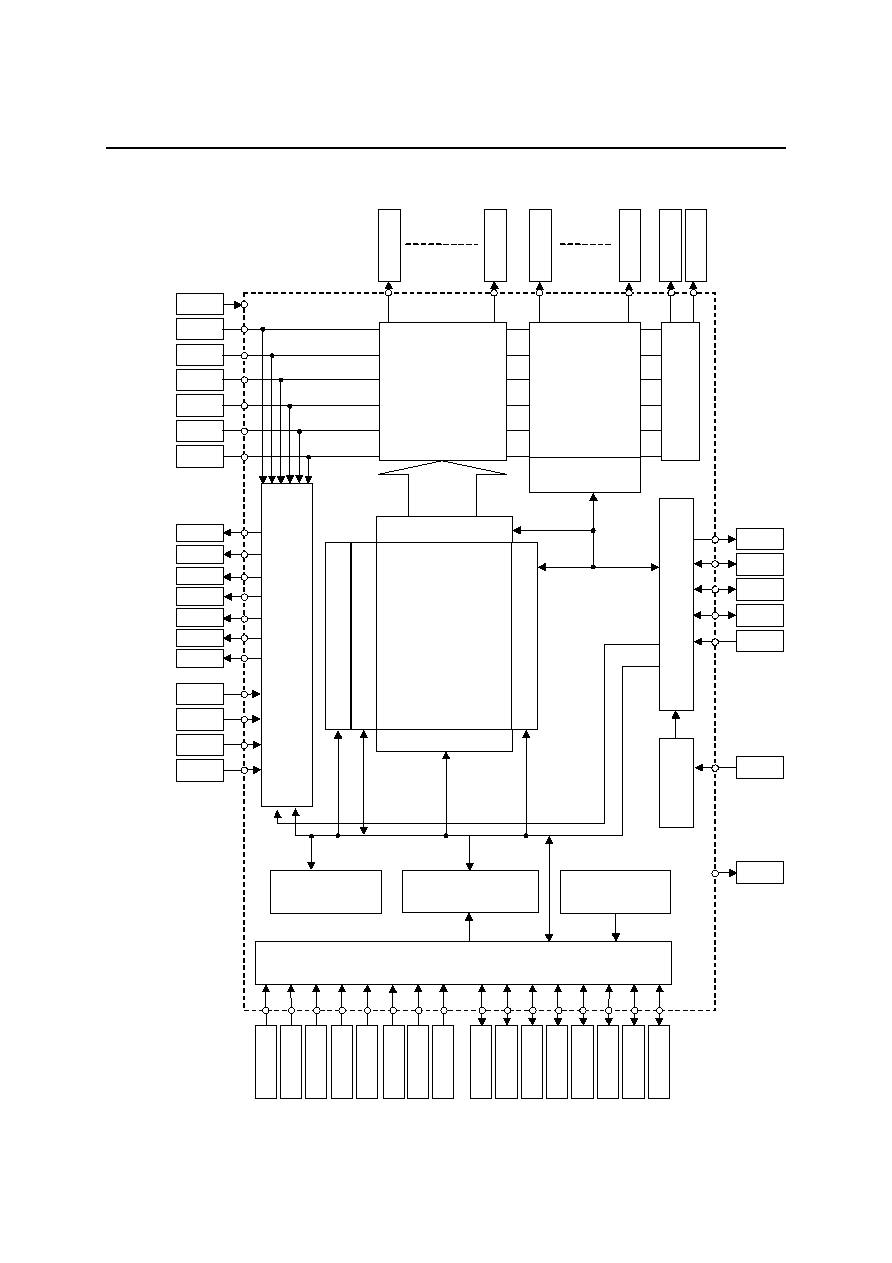
GENERAL DESCRIPTION
The ML9059 is an LSI for dot matrix graphic LCD devices carrying out bit map display. This LSI can drive a dot
matrix graphic LCD display panel under the control of an 8-bit microcomputer (hereinafter described MPU).
Since all the functions necessary for driving a bit map type LCD device are incorporated in a single chip, using the
ML9059 makes it possible to realize a bit map type dot matrix graphic LCD display system with only a few chips.
Since the bit map method in which one bit of display RAM data turns ON or OFF one dot in the display panel, it is
possible to carry out displays with a high degree of freedom such as Chinese character displays, etc. With one chip,
it is possible to construct a graphic display system with a maximum of 49
◊ 132 dots. The display can be expanded
further using two chips. However, the ML9059 is not used in a multiple chip configuration when a line reversal
drive is set.
The ML9059 is made using a CMOS process. Because it has a built-in RAM, low power consumption is one of its
features, and is therefore suitable for displays in battery-operated portable equipment.
The ML9059 has 49 common signal outputs and 132 segment signal outputs and one chip can drive a display of up
to 49
◊ 132 dots.
FEATURES
∑ Direct display of the RAM data using the bit map method
Display RAM data "1" ... Dot is displayed
Display RAM data "0" ... Dot is not displayed (during forward display)
∑ Display RAM capacity
65
◊ 132 = 8580 bits
∑ LCD Drive circuits
49 common outputs, 132 segment outputs
∑ MPU interface: Can select an 8-bit parallel or serial interface
∑ Built-in voltage multiplier circuit for the LCD drive power supply
∑ Built-in LCD drive voltage adjustment circuit
∑ Built-in LCD drive bias generator circuit
∑ Can select frame reversal drive or line reversal drive by command
∑ Built-in oscillator circuit (Internal RC oscillator/external clock input)
∑ A variety of commands
Read/write of display data, display ON/OFF, forward/reverse display, all dots ON/all dots OFF, set page address,
set display start address, etc.
∑ Power supply voltage
Logic power supply: VDD-VSS = 3.7 V to 5.5 V
Voltage multiplier reference voltage: VIN-VSS = 3.7 V to 5.5 V
(2- to 4-time multiplier available)
LCD Drive voltage: VBI-VSS = 6.0 to 18 V
∑ Package : Gold bump chip (Bump hardness: Low, DV)
: Gold bump chip (Bump hardness: High, CV)
∑ This device is not resistant to radiation and light.
PEDL9059-02
OKI Semiconductor
ML9059
3/72
ABSOLUTE MAXIMUM RATINGS
V
SS
= 0 V
Parameter
Symbol
Condition
Rated value
Unit
Applicable pins
Power supply voltage
V
DD
Tj = 25∞C
≠0.3 to +6.5
V
V
DD
Bias voltage
V
BI
Tj = 25∞C
≠0.3 to +20
V
V1 to V5
Voltage multiplier output
voltage
V
OUT
Tj = 25∞C
≠0.3 to +20
V
V
OUT
Voltage multiplier reference
voltage
V
IN
2-time multiplication
3-time multiplication
4-time multiplication
≠0.3 to +5.5
≠0.3 to +5.5
≠0.3 to +5.0
V V
IN
Input voltage
V
I
Tj = 25∞C
≠0.3 to V
DD
+0.3 V All
inputs
Storage temperature range
T
STG
Chip
≠55 to +125
∞C
--
Tj: Chip surface temperature
RECOMMENDED OPERATING CONDITIONS
V
SS
= 0 V
Parameter
Symbol
Condition
Rated value
Unit
Applicable pins
Power supply voltage
V
DD
--
3.7 to 5.5
V
V
DD
Bias voltage
V
BI
--
6 to 18
V
V1 to V5
Voltage multiplier reference
voltage
V
IN
2-time multiplication
3-time multiplication
4-time multiplication
3.7 to 5.5
3.7 to 5.5
3.7 to 4.5
V V
IN
Voltage multiplier output
voltage
V
OUT
External input
6.0 to 18
V
V
OUT
Operating temperature range
T
JOP
--
≠40 to +85
∞C
--
Note 1: The electrical characteristics are influenced by COG trace resistance. This LSI always has to be evaluated
before using.
Note 2: The voltages V
DD
, V1 to V5, and V
OUT
are values taking V
SS
= 0 V as the reference.
Note 3: The highest bias potential is V1 and the lowest is V
SS
.
Note 4: Always maintain the relationship V1
V2 V3 V4 V5 V
SS
among these voltages.
V
CC
GND
V
IN
V
DD
V
SS
V
OUT
V1 to V5
ML9059
System (MPU)

PEDL9059-02
OKI Semiconductor
ML9059
4/72
Note 5: When using an external power supply, follow the procedure for power application.
When applying external power to the V
OUT
pin only, apply V
OUT
after V
DD.
When applying external power to the V1 pin only, apply V1 after V
DD
.
When applying external power to the V1 pin to V5 pin, apply V1 to V5 after V
DD
.
Note that the above (Note 4) must be satisfied including transient state at power application.
Note 6: When using an external power supply, follow the procedure for power removal described below.
When external power is in use for the V
OUT
pin only, remove V
OUT
after V
DD
.
When external power is in use for the V1 pin only, remove V1 after V
DD
.
When external power is in use for the V1 pin to V5 pin, remove V1 to V5 after V
DD
.
Note that the above (Note 4) must be satisfied including transient state at power removal.
PEDL9059-02
OKI Semiconductor
ML9059
5/72
ELECTRICAL CHARACTERISTICS
DC Characteristics
[V
SS
= 0 V, V
DD
= 3.7 to 5.5 V, Tj =≠40 to +85∞C]
Parameter Symbol
Condition Min
Typ
Max
Unit
Applicable
pins
"H" Input voltage
V
IH
0.8
◊ V
DD
-- V
DD
"L" Input voltage
V
IL
0
--
0.2
◊ V
DD
V *1
"H" Input voltage
V
IH
0.8
◊ V
DD
-- V
DD
"L" Input voltage
V
IL
0
--
0.2
◊ V
DD
Hysteresis width
V V
DD
= 5.0 V
--
1.0
--
V *2
"H" output voltage
V
OH
I
OH
= ≠0.5 mA
0.8
◊ V
DD
-- --
"L" output voltage
V
OL
I
OL
= 0.5 mA
--
--
0.2
◊ V
DD
V *3
"H" Input current
I
IH
V
I
= V
DD
≠1.0
--
+1.0
"L" Input current
I
IL
V
I
= 0 V
≠3.0
--
+3.0
µA *4
*5
V1 output voltage
temperature gradient
V1TC
Tj = 25∞C
V1 = 12 V
-- ≠0.05
-- %/∞C V1
Reference voltage
V
REG
Tj
=
25∞C 2.925
3.00
3.075
V V
RS
V1 output voltage
V1
*6
10.58
10.85
11.12
V
V1
3-time
multiplication *7
13.0 -- -- V V
OUT
Voltage multiplier
output voltage
V
OUT
4-time
multiplication *8
15.9 -- -- V V
OUT
V
OUT
- V1 voltage
Vot1
*9
0.6
--
--
V
V
OUT,
V1
LCD driver ON
resistance
R
ON
I
O
= ±50 µA
--
--
10
k
SEG1 to 131,
COMS0,
COMS1,
COM0 to 47
27 33 39 kHz *10
Internal
oscillation
f
OSC
Tj
=
25∞C
21 -- 47
kHz
Oscillator
frequency
External
input
f
EXT
14
17
20
kHz
CL*10
*1: DB0 to DB5, DB7 (SI), FR, DOF Pins
*2: A0, CS1, CS2, CLS, M/S, C86, P/S, IRS,RD (E), WR (R/W), RES, CL, DB6 (SCL) Pins
*3: DB0 to DB7, FR, FRS, DOF, CL Pins
*4: A0,
RD (E), WR (R/W), CS1, CS2, CLS, M/S, C86, P/S, RES, IRS Pins
*5: Applicable to the pins DB0 to DB5, DB6 (SCL), DB7 (SI), CL, FR, DOF in the high impedance state.
*6: Tj = 25∞C,
= 31, (1+Rb/Ra) = 4, V
OUT
= 13.5 V (External input), LCD drive output = no-load
*7: V
IN
= 4.8 V, voltage multiplier capacitor C1 = 2.6 to 4.0
µF, voltage multiplier output load current
I = 500
µA. Only a voltage multiplier circuit operates, not activating the voltage adjustment circuit and V/F
circuit, by command "2C".
*8: V
IN
= 4.5 V, voltage multiplier capacitor C1 = 2.6 to 4.0
µF, voltage multiplier output load current
I = 500
µA. Only a voltage multiplier circuit operates, not activating the voltage adjustment circuit and V/F
circuit, by command "2C".