 | –≠–ª–µ–∫—Ç—Ä–æ–Ω–Ω—ã–π –∫–æ–º–ø–æ–Ω–µ–Ω—Ç: ML9204 | –°–∫–∞—á–∞—Ç—å:  PDF PDF  ZIP ZIP |

OKI Semiconductor
PEDL9204-02
Issue Date: Oct. 12, 2004
ML9204-xx
Preliminary
5
◊
7 Dot Character
◊
24-Digit
◊
2-Line Display Controller/Driver with Character RAM (Built-in Key Scan)
1/41
GENERAL DESCRIPTION
The ML9204-xx is a 5
◊
7 dot matrix type vacuum fluorescent display tube controller driver IC which displays
characters, numerics and symbols of a maximum of 24 digits
◊
2 lines.
Dot matrix vacuum fluorescent display tube drive signals are generated by serial data sent from a
micro-controller. A display system is easily realized by internal ROM and RAM for character display.
Built-in key scan for 3-channel encoder type rotary switch and 5
◊
6 matrix key switch allow the user to receive
each switch input.
The ML9204-xx has low power consumption since it is made by CMOS process technology.
≠01 is available as a general-purpose code.
Custom codes are provided on customer's request.
FEATURES
∑
Logic power supply (V
DD
)
: 3.3 V±10% or 5.0 V±10%
∑
VFD tube drive power supply (V
SEG
, V
COM
) : 20 to 60 V
∑
VFD driver output current
(VFD driver output can be connected directly to the VFD tube. No pull-down resistor is required.)
∑ Segment driver (SEGA1 to A35, SEGB1 to B35)
Only one driver output is high
: ≠5 mA (V
SEG
= 60 V)
All the driver outputs are high
: ≠350 mA (V
SEG
= 60 V)
∑ Segment driver (ADA, ADB)
: ≠15 mA (V
SEG
= 60 V)
∑ Grid driver (COM1 to 24)
: ≠25 mA (V
COM
= 60 V)
∑
Content of display
SEGA1 to SEGA35 and ADA
∑ CGROM_A
:
5
◊
7 dots 240 types (character data)
∑ CGRAM_A
:
5
◊
7 dots 16 types (character data)
∑ ADRAM_A
: 24 (display digit)
◊
1 bit (symbol data; can be used for a cursor.)
∑ DCRAM_A
: 24 (display digit)
◊
8 bits (register for character data display)
SEGB1 to SEGB35 and ADB
∑ CGROM_B
:
5
◊
7 dots 240 types (character data)
∑ CGRAM_B
:
5
◊
7 dots 16 types (character data)
∑ ADRAM_B
: 24 (display digit)
◊
1 bit (symbol data; can be used for a cursor.)
∑ DCRAM_B
: 24 (display digit)
◊
8 bits (register for character data display)
∑
Display control function
∑ GCRAM
: Simultaneous output of COM1 to 24 can be set in 1 grid.
∑ Display digits
: 1 to 24 digits (9- to 24-bit arbitrary setting)
∑ Display duty (brightness adjustment)
: 0/1024 to 960/1024 stages
∑ All lights ON/OFF
∑
5 interfaces with microcontroller:DI/O,
CS, CP, RESET, INT
∑
Built-in key scan circuit for 5
◊
6 matrix key switch
∑
Built-in key scan circuit for 3-channel encoder type rotary switch
∑
Built-in oscillation circuit
Crystal oscillation or ceramic oscillation: 4.0 MHz (Typ)
∑
Standby function
Inhibiting the oscillator circuit provides low power consumption.
∑
Package options:
128-pin plastic QFP (QFP128-P-1420-0.50-K) (ML9204-xxGA)
PEDL9204-02
OKI Semiconductor
ML9204-xx
2/41
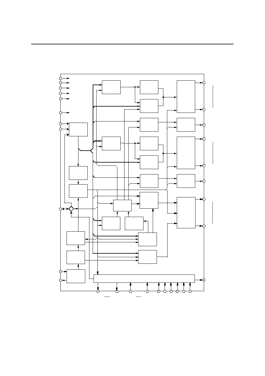
BLOCK DIAGRAM
V
COM
V
DD
D-GND
RESET
CP
CS
OSC0
OSC1
SEGA1
SEGA35
ADA
COM1
COM24
DCRAM_A
24w
◊
8b
CGROM_A
240w
◊
35b
CGRAM_A
16w
◊
35b
ADRAM_B
24w
◊
1b
Command
Decoder
Control
Circuit
Timing
Generator 1
Oscillator
Digit
Control
Duty
Control
Grid
Driver
Segment
Driver
Write
Address
Counter
Read
Address
Counter
Address
Selector
Segment
Driver
SEGB1
SEGB35
ADB
DCRAM_B
24w
◊
8b
CGROM_B
240w
◊
35b
CGRAM_B
16w
◊
35b
ADRAM_B
24w
◊
1b
Segment
Driver
Segment
Driver
Timing
Generator 2
L-GND
5 x 6 Key Scan and Encoder Switch Interface
INT
B3
A3
B2
A2
B1
A1
COL
6
COL
1
ROW5
ROW1
GCRAM
24w
◊
24b
V
SEG
DI/O
8bit Shift
Register
PEDL9204-02
OKI Semiconductor
ML9204-xx
3/41
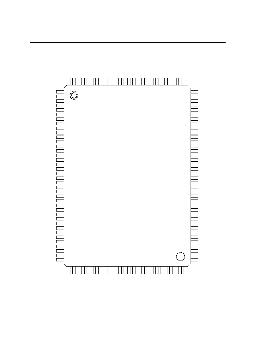
PIN CONFIGURATION (TOP VIEW)
108
107
106
105
104
103
S
E
G
B
27
S
E
G
B
28
S
E
G
B
29
S
E
G
B
30
S
E
G
B
31
S
E
G
B
32
128
127
126
125
124
123
122
121
120
1
19
1
18
1
17
1
16
1
15
1
14
1
13
1
12
111
1
10
1
09
SE
G
B
7
SE
G
B
8
SE
G
B
9
S
E
G
B
10
SE
G
B
1
1
S
E
G
B
12
S
E
G
B
13
S
E
G
B
14
S
E
G
B
15
S
E
G
B
16
S
E
G
B
17
S
E
G
B
18
S
E
G
B
19
S
E
G
B
20
S
E
G
B
21
S
E
G
B
22
S
E
G
B
23
S
E
G
B
24
S
E
G
B
25
S
E
G
B
26
39
40
41
42
43
44
45
46
47
48
49
50
51
52
53
54
55
56
57
58
SE
G
A
7
SE
G
A
8
SE
G
A
9
S
E
G
A
10
SE
G
A
11
S
E
G
A
12
S
E
G
A
13
S
E
G
A
14
SE
G
A
1
5
SE
G
A
1
6
S
E
G
A
17
S
E
G
A
18
S
E
G
A
19
S
E
G
A2
0
S
E
G
A
21
S
E
G
A
22
S
E
G
A
23
S
E
G
A
24
S
E
G
A
25
S
E
G
A
26
59
S
E
G
A
27
60
S
E
G
A
28
61
S
E
G
A
29
62
S
E
G
A
30
63
S
E
G
A
31
64
S
E
G
A
32
1
2
3
4
5
6
7
8
9
10
11
12
13
14
15
16
17
18
19
20
21
22
23
24
25
26
27
28
29
30
SEGB6
SEGB5
SEGB4
SEGB3
SEGB2
V
COM
COM1
COM2
COM3
COM4
COM5
COM6
COM7
COM8
COM9
COM10
COM11
COM12
COM13
COM14
COM15
COM16
COM17
COM18
COM19
COM20
COM21
COM22
COM23
SEGB1
31
32
33
34
35
36
37
38
COM24
V
COM
SEGA2
SEGA3
SEGA4
SEGA5
SEGA6
SEGA1
102
101
100
99
98
97
96
95
94
93
92
91
90
89
88
87
86
85
84
83
82
81
80
79
78
77
76
75
74
73
ADB
SEGB33
SEGB34
SEGB35
V
SEG
D-GND
V
DD
INT
DI/O
CP
CS
RESET
B3
A3
B2
A2
B1
A1
COL
6
COL
5
COL
4
COL
3
COL
2
COL
1
ROW5
ROW4
ROW3
ROW2
ROW1
OSC1
ADA
72
71
70
69
68
67
66
65
OSC0
L-GND
D-GND
V
SEG
SEGA35
SEGA34
SEGA33
128-Pin Plastic QFP
PEDL9204-02
OKI Semiconductor
ML9204-xx
4/41
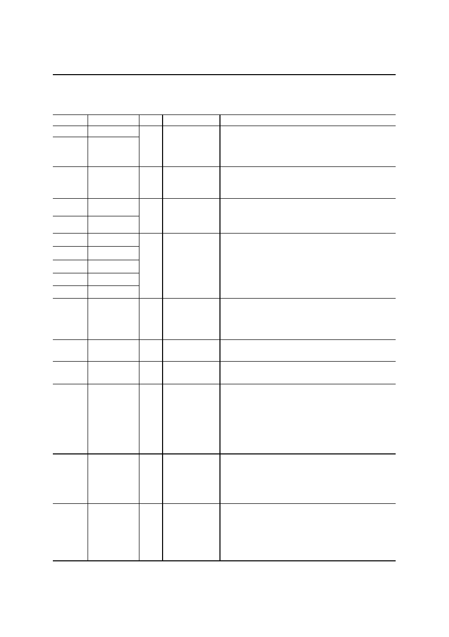
PIN DESCRIPTION
Pin Symbol
Type
Connects
to
Description
33 to 67 SEGA1 to A35
1 to 6
100 to
128
SEGB1 to B35
O
VFD tube anode
electrode
VFD tube anode electrode drive output.
Directly connected to fluorescent display tube and a
pull-down resistor is not necessary. I
OH
< ≠5 mA
8 to 31
COM1 to 24
O
VFD tube grid
electrode
VFD tube grid electrode drive output.
Directly connected to fluorescent display tube and a
pull-down resistor is not necessary. I
OH
< ≠25 mA
68 ADA
99 ADB
O
VFD tube anode
electrode
VFD tube anode electrode drive output.
Directly connected to fluorescent display tube and a
pull-down resistor is not necessary. I
OH
< ≠15 mA
96 V
DD
71 L-GND
7,32 V
COM
69,98 V
SEG
70,97 D-GND
-- Power
supply
V
DD
-L-GND are power supplies for internal logic.
V
COM
-D-GND are power supplies for driving VFD tube
grid.
V
COM
-D-GND are power supplies for driving VFD tube
anode.
Use the same power supply for L-GND and D-GND.
94 DI/O
I/O
Micro
controller
Serial data input-output (positive logic).
Data is input and output to sift register synchronized
with the rise of shift clock.
When Inputting data input from the LSB.
93
CP
l Micro
controller
Shift clock input.
Serial data is shifted on the rising edge of
CP
.
92
CS
l Micro
controller
Chip select input.
Serial data transfer is disabled when
CS
pin is "H" level.
95 INT
O
Micro
controller
Output pin for interrupt signal to micro controller.
When depression or release of key matrix switch is
detected, key scanning starts and when 1 cycle is
completed, this pin becomes high level. Upon receiving
encoder type rotary switch input, this pin becomes high
level. The INT pin remains at high level until the key
scan stop mode is selected..
85,86
87,88
89,90
A1,B1
A2,B2
A3,B3
l Rotary
switch
Encoder type rotary switch input pins.
All inputs possess chattering absorption function of
256us period.
Those inputs must be tied to ground when they are
not used.
79 to 84
COL
1 to 6
I
Key matrix
Input pins for return signal from key matrix with built-in
pull-up resister.
When input is low level, the key matrix switch is
regarded as being pressed.
Dose not have chattering absorption function.
PEDL9204-02
OKI Semiconductor
ML9204-xx
5/41
74 to 78
ROW1 to 5
O
Key matrix
Key matrix scan signal output pins.
Normally low level is output.
Key scanning starts by detecting depression or release
of key matrix switch and continues until selection of key
scan stop mode.
When key scan stop mode is selected, all outputs of
ROW1 to 5 return to low level.
91
RESET
l Micro
controller
Reset input.
"Low" initializes all the functions.
Initial status is as follows.
∑ Address of each RAM .............. address "00"H
∑ Data of each RAM ................... Content is undefined
∑ Display digit............................. 24 digits
∑ Brightness adjustment ............. 0/1024
∑ All lights ON or OFF ................ OFF mode
∑ ROW1 to 5 .............................. becomes low level
∑ INT.......................................... becomes low level
72 OSC0 l
73 OSC1
O
Crystal or
ceramic
resonator
Pins for self-oscillation.
(Do not apply external clocks to these pins.)
Connect these pins to the crystal and capacitors or to
the ceramic resonator and capacitors.
The target oscillation frequency is 4.0MHz.
(The device has an internal feedback resister.)
V
DD
Typical
3.3V 1Mohm
5.0V 0.4Mohm
* For information regarding the oscillator contact the
manufacturer of the oscillator.
* As regards the circuit, refer to the Application Circuit.
PEDL9204-02
OKI Semiconductor
ML9204-xx
6/41
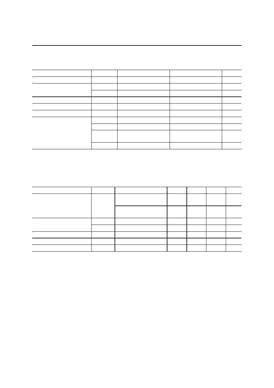
ABSOLUTE MAXIMUM RATINGS
Parameter Symbol
Condition
Rating Unit
Supply Voltage (1)
V
DD
--
≠0.3 to +6.5
V
V
SEG
--
≠0.3 to +70
V
Supply Voltage (2)
V
COM
--
≠0.3 to +70
V
Input Voltage
V
IN
--
≠0.3 to V
DD
+0.3 V
Power Dissipation
P
D
Ta
85∞C
470 *1)
mW
Storage Temperature
T
STG
--
≠55 to +150
∞C
l
O1
COM1 to COM24
≠50 to +2.0
mA
l
O2
ADA, ADB
≠30 to +2.0
mA
l
O3
SEGA1 to SEGA35,
SEGB1 to SEGB35
≠10 to +2.0
mA
Output Current
I
O4
ROW1 to 5 / INT
≠2.0 to +2.0
mA
*1) When use two or more COM, be careful of the following things.
The junction temperature which can be found by the following formula does not exceed 120.
Tj = (Px 85∞C /W)+Ta (P is the maximum power consumption of IC.)
RECOMMENDED OPERATING CONDITIONS
Parameter Symbol Condition Min.
Typ.
Max.
Unit
When the power supply
voltage is 5.0 V (typ.)
4.5 5.0 5.5 V
Supply Voltage (1)
V
DD
When the power supply
voltage is 3.3 V (typ.)
3.0 3.3 3.6 V
V
SEG
-- 20
--
60
V
Supply Voltage (2)
V
COM
-- 20
--
60
V
Operating Frequency
f
OSC
Oscillation 3.5
4.0
4.5
MHz
Frame Frequency
f
FR
DIGIT = 1 to 24, oscillation
142 163 183 Hz
Operating Temperature
T
OP
--
≠40 -- +85 ∞C
PEDL9204-02
OKI Semiconductor
ML9204-xx
7/41
ELECTRICAL CHARACTERISTICS
DC Characteristics (V
DD
= 5.0 V±10%)
(V
DD
= 5.0 V±10%, V
SEG
and V
COM
= 20 to 60 V, Ta = ≠40 to +85∞C, unless otherwise specified)
Parameter Symbol
Applied
pin
Condition
Min.
Max.
Unit
High Level Input Voltage
V
IH
*1
V
DD
= 5.0 V±10%
0.7 V
DD
-- V
Low Level Input Voltage
V
IL
*1
V
DD
= 5.0 V±10%
--
0.3 V
DD
V
High Level Input Current
I
IH
*1
V
IH
= V
DD
≠1.0
+1.0
µ
A
I
IL1
*2
V
IL
= 0.0 V
≠1.0
+1.0
µ
A
Low Level Input Current
I
IL2
COL1 to 6
V
DD
= 5.0 V±10%, V
IL
= 0.0 V
≠450
≠100
µ
A
V
OH1
COM1 to 24
V
COM
= 60 V, I
OH1
= ≠25 mA V
COM
≠ 2.0
--
V
V
OH2
ADA,
ADB V
SEG
= 60 V, I
OH2
= ≠15 mA
V
SEG
≠ 2.0
--
V
V
OH3
SEGA1 to A35
SEGB1 to B35
V
SEG
= 60 V, I
OH3
= ≠5 mA
V
SEG
≠ 2.0
--
V
High Level Output
Voltage
V
OH4
INT, ROW1 to 5
V
DD
= 5.0 V±10%, I
OH4
= ≠450
µ
A
V
DD
≠ 0.2
--
V
V
OL1
*3
--
--
1.0
V
Low Level Output
Voltage
V
OL2
INT, ROW1 to 5 V
DD
=5.0 V±10%, I
OL2
= 450
µ
A
-- 0.2
V
I
DD1
V
DD
V
DD
= 5.0 V±10%, f
OSC
= 4.0
MHz
-- 6.0
mA
I
DISP1
All output lights ON
--
1.0
mA
Supply Current (1)
I
DISP2
V
SEG,
V
COM
f
OSC
= 4.0
MHz,
no load
All output lights OFF
--
200
µ
A
I
DDS
V
DD
--
1.0
µ
A
Supply Current (2)
I
DISPS
V
SEG,
V
COM
In standby mode
--
20.0
µ
A
*1)
CS
,
CP
, DI/O,
RESET
,
COL
1 to 6
*2)
CS
,
CP
, DI/O,
RESET
*3) SEGA1 to A35, SEGB1 to B35, ADA, ADB, COM1 to 24

PEDL9204-02
OKI Semiconductor
ML9204-xx
8/41
DC Characteristics (V
DD
= 3.3 V±10%)
(V
DD
= 3.3 V±10%, V
SEG
and V
COM
= 20 to 60 V, Ta = ≠40 to +85∞C, unless otherwise specified)
Parameter Symbol
Applied
pin
Condition
Min.
Max.
Unit
High Level Input Voltage
V
IH
*1
V
DD
= 3.3 V±10%
0.8 V
DD
-- V
Low Level Input Voltage
V
IL
*1
V
DD
= 3.3 V±10%
--
0.2
V
DD
V
High Level Input Current
I
IH
*1
V
IH
= V
DD
≠1.0
+1.0
µ
A
I
IL1
*2
V
IL
= 0.0 V
≠1.0
+1.0
µ
A
Low Level Input Current
I
IL3
COL1 to 6
V
DD
= 3.3 V±10%, V
IL
= 0.0 V
≠120
≠25
µ
A
V
OH1
COM1 to 24
V
COM
= 60 V, I
OH1
= ≠25 mA V
COM
≠ 2.0
--
V
V
OH2
ADA,
ADB V
SEG
= 60 V, I
OH2
= ≠15 mA
V
SEG
≠ 2.0
--
V
V
OH3
SEGA1 to A35
SEGB1 to B35
V
SEG
= 60 V, I
OH3
= ≠5 mA
V
SEG
≠ 2.0
--
V
High Level Output
Voltage
V
OH5
INT, ROW1 to 5
V
DD
= 3.3 V±10%, I
OH5
= ≠120
µ
A
V
DD
≠ 0.2
--
V
V
OL1
*3
--
--
1.0
V
Low Level Output
Voltage
V
OL2
INT, ROW1 to 5 V
DD
= 3.3 V±10%, I
OL3
= 120
µ
A
-- 0.2
V
I
DD2
V
DD
V
DD
= 3.3 V±10%, f
OSC
= 4.0
MHz
-- 4.0
mA
I
DISP1
All output lights ON
--
1.0
mA
Supply Current (1)
I
DISP2
V
SEG,
V
COM
f
OSC
= 4.0
MHz,
no load
All output lights OFF
--
200
µ
A
I
DDS
V
DD
--
1.0
µ
A
Supply Current (2)
I
DISPS
V
SEG,
V
COM
In standby mode
--
20.0
µ
A
*1)
CS
,
CP
, DI/O,
RESET
,
COL
1 to 6
*2)
CS
,
CP
, DI/O,
RESET
*3) SEGA1 to A35, SEGB1 to B35, ADA, ADB, COM1 to 24

PEDL9204-02
OKI Semiconductor
ML9204-xx
9/41
AC Characteristics
(V
DD
= 5.0 V±10%, or V
DD
= 3.3 V±10%,V
SEG
and V
COM
= 20 to 60 V, T
a
= ≠40 to +85∞C unless otherwise specified)
Parameter Symbol
Condition
Min.
Max.
Unit
CP
Frequency
f
C
--
--
2.0
MHz
CP
Pulse Width
t
CW
--
200
--
ns
D/A Setup Time
t
DS
--
200
--
ns
D/A Hold Time
t
DH
--
200
--
ns
CS
Setup Time
t
CSS
--
200
--
ns
CS
Hold Time
t
CSH
Oscillating
state 8
--
µ
s
CS
Wait Time
t
CSW
--
200
--
ns
Data Processing Time
t
DOFF
Oscillating
state 4
--
µ
s
RESET
Pulse Width
t
WRES
When
RESET
signal is input from
microcontroller etc. externally
200 -- ns
RESET
Time
t
RSON
--
t
OSCON
--
D/A Wait Time
t
RSOFF
-- 200
--
ns
t
R
t
R
= 20 to 80%
--
2.0
µ
s
All Output Slew Rate
t
F
C
l
= 100 pF
t
F
= 80 to 20%
--
2.0
µ
s
OSC Duty Ratio
du
OSC
-- 40
60
%
Oscillation Rise Time
t
OSCON
--
*1
*1 t
OSCON
(oscillation rise time) differs with the oscillator pin used.
As regards oscillation rise time, refer to the data of oscillator used.
Key Scan Characteristics
(V
DD
= 5.0V±10%, or V
DD
= 3.3V±10%, V
SEG
and V
COM
= 20 to 60 V, T
a
= ≠40 to +85∞C unless otherwise specified)
Parameter Symbol Condition Min.
Typ.
Max.
Unit
Key Scan Time
t
SCAN
142.2
160
182.8
µ
s
Key Scan Pulse Width
t
WSCAN
f
OSC
= 3.5 to 4.5 MHz
28.4 32 36.6
µ
s
Rotary Switch Characteristics
(V
DD
= 5.0V±10%, or V
DD
= 3.3V±10%, V
SEG
and V
COM
= 20 to 60 V, T
a
= ≠40 to +85∞C unless otherwise specified)
Parameter Symbol Condition Min.
Typ.
Max.
Unit
Phase Input Time
t
ABW
Phase Input Fixed Time
t
ABH
f
OSC
= 3.5 to 4.5 MHz
1.2
--
--
ms
PEDL9204-02
OKI Semiconductor
ML9204-xx
10/41
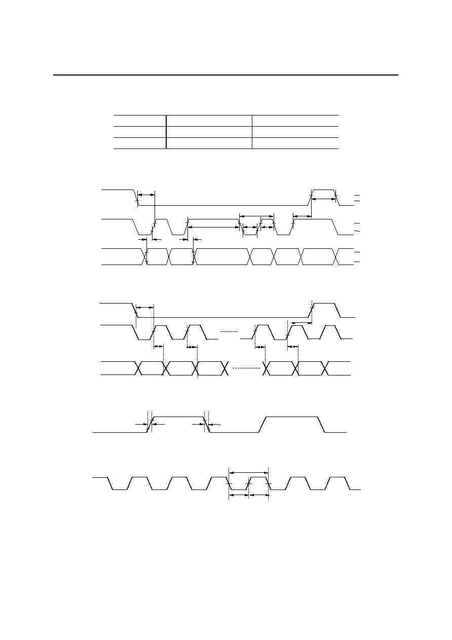
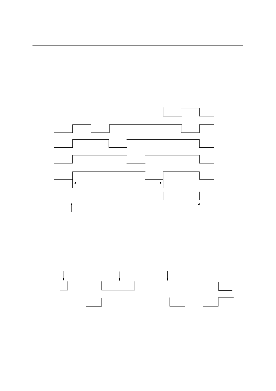
TIMING DIAGRAMS
Symbol V
DD
= 5.0 V ±10%
V
DD
= 3.0 V ±10%
V
IH
0.7
V
DD
0.8
V
DD
V
IL
0.3
V
DD
0.2
V
DD
Data Input Timing
Data Output Timing
Output Timing
5)
OSC Timing
CS
CP
DI/O
(INPUT)
t
CSS
t
DS
t
DH
t
DOFF
t
CW
VALID
VALID
VALID VALID
V
IH
V
IH
V
IL
V
IL
V
IH
V
IL
1/f
C
t
CW
t
CSH
t
CSW
CS
CP
DI/O
t
CSS
t
CSH
≠V
IH
≠V
IL
≠V
IH
≠V
IL
≠V
IH
≠V
IL
(OUTPUT)
VALID
VALID
T
PD
T
PD
VALID
T
PD
T
PD
VALID
VALID
≠0.8 (V
SEG,
V
COM
)
t
F
t
R
≠0.2 (V
SEG,
V
COM
)
All Output Driver
-0.5VDD
du
OSC
=Bx100/(A+B)
OSC1
A
B

PEDL9204-02
OKI Semiconductor
ML9204-xx
11/41
Standby Mode Release Timing
Reset Timing
* After a VDD injection should surely input a reset signal.
Key Scan Timing
CS
CP
OSC0
≠V
IH
≠V
IL
200nsec or more
0.9Vp-p
Vp-p (stationary state oscillation level)
DI/O
VALID
≠V
IH
≠V
IL
≠V
IH
≠V
IL
t
RSON
t
OSCON
V
DD
RESET
DI/O
t
RSON
≠0.8 V
DD
≠V
IH
≠0.0 V
≠V
IL
t
RSOFF
t
WRES
VALID
≠V
IH
≠V
IL
ROW1
ROW5
ROW2
ROW3
ROW4
t
SCAN
t
WSCAN
PEDL9204-02
OKI Semiconductor
ML9204-xx
12/41
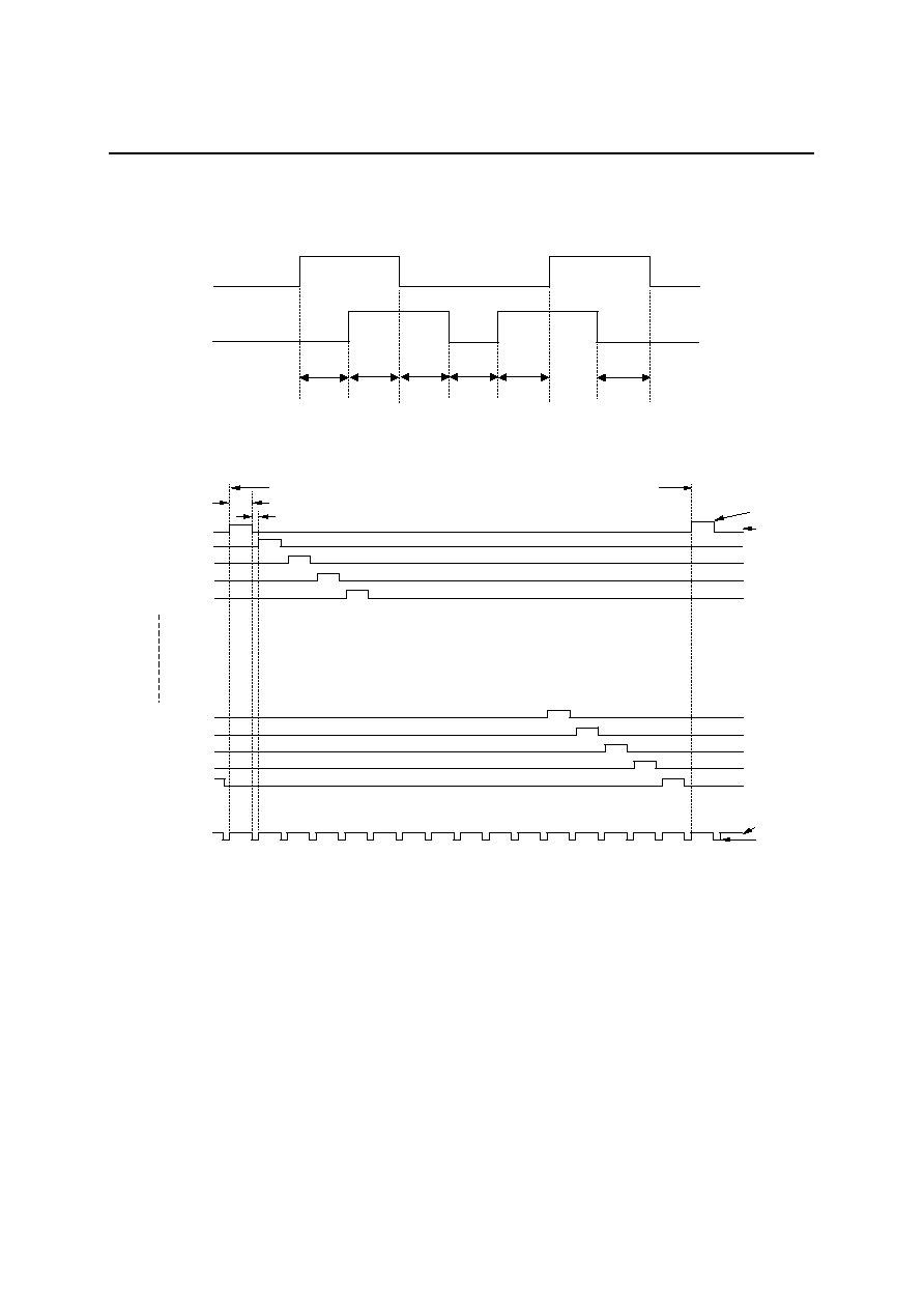
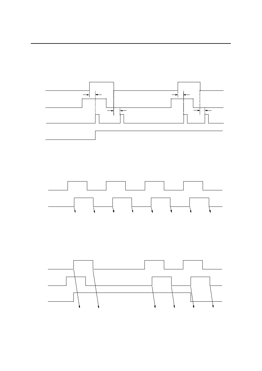
Rotary Switch Input Timing
Digit Output Timing (24-Digit,960/1024-Duty)
A
B
t
ABH
t
ABW
t
ABH
t
ABW
t
ABW
COM1
COM2
COM3
COM4
COM5
COM20
COM21
COM22
COM23
COM24
ADA, ADB,
SEGA1~A35,
SEGB1~B35
D-GND
t
1
= 24576T
t
2
= 960T
t
3
= 64T
Frame cycle
Display
Blank Timing
V
COM
D-GND
V
SEG
*:
T = 1/f
OSC
(f
OSC
= 4.0 MHz : t
1
= 6.144ms)
(f
OSC
= 4.0 MHz : t
2
= 240µs)
(f
OSC
= 4.0 MHz : t
3
= 16µs)

PEDL9204-02
OKI Semiconductor
ML9204-xx
13/41
FUNCTIONAL DESCRIPTION
Commands List
LSB 1st byte
MSB
LSB 2nd byte
MSB
Command
B0 B1 B2 B3 B4 B5 B6 B7 B0 B1 B2 B3 B4 B5 B6 B7
1 DCRAM_A
data
write
* * * *
1
0
0
0 C0 C1 C2 C3 C4 C5 C6 C7
C0 C5 C10 C15 C20 C25 C30 * 2nd
byte
C1 C6 C11 C16 C21 C26 C31 * 3rd
byte
C2 C7 C12 C17 C22 C27 C32 * 4th
byte
C3 C8 C13 C18 C23 C28 C33 * 5th
byte
2
CGRAM_A data write
0
0
0
0
0
1
0
0
C4 C9 C14 C19 C24 C29 C34 * 6th
byte
3
ADRAM_A data write
*
*
*
*
1
1
0
0 C0
*
*
*
*
*
*
*
C0 C1 C2 C3 C4 C5 C6 C7
C8 C9 C10 C11 C12 C13 C14 C15
4
GCRAM data write
*
*
*
*
0
0
1
0
C16 C17 C18 C19 C20 C21 C22 C23
5
Display duty set
D0 D1
*
*
1
0
1
0 D2 D3 D4 D5 D6 D7 D8 D9
6 Number of digits set K0 K1 K2 K3
0
1
1
0
7 All lights ON/OFF
L H * *
1
1
1
0
9 DCRAM_B
data
write
* * * *
1
0
0
1 C0 C1 C2 C3 C4 C5 C6 C7
C0 C5 C10 C15 C20 C25 C30 * 2nd
byte
C1 C6 C11 C16 C21 C26 C31 * 3rd
byte
C2 C7 C12 C17 C22 C27 C32 * 4th
byte
C3 C8 C13 C18 C23 C28 C33 * 5th
byte
A
CGRAM_B data write
0
0
0
0
0
1
0
1
C4 C9 C14 C19 C24 C29 C34 * 6th
byte
B
ADRAM_B data write
*
*
*
*
1
1
0
1 C0
*
*
*
*
*
*
*
C Key scan stop
* * * *
0
0
1
1
D
Key data output
*
*
*
*
1
0
1
1
Refer to item D of command and
function description.
F Standby
mode
* * * *
1
1
1
1
0 Test Mode(Note)
0
0
0
0
When data is written to RAM (DCRAM, CGRAM,
ADRAM, and GCRAM) continuously, addresses are
internally incremented automatically.
Therefore it is not necessary to specify the 1st byte to write
RAM data for the 2nd and later bytes.
*
: Don't care
Xn : Address specification for each RAM
Cn : Character code specification for each RAM
Dn : Display duty specification
Kn : Number of digits specification
H : All lights ON instruction
L : All lights OFF instruction
Note: The test mode is used for inspection before shipment.
It is not a user function. The user cannot use this
command. Enter commands 1 to 7, 9 to D, and
F alone in the way described on the next page and the
following pages. (The operation of this device cannot be
guaranteed if other commands are used.
PEDL9204-02
OKI Semiconductor
ML9204-xx
14/41
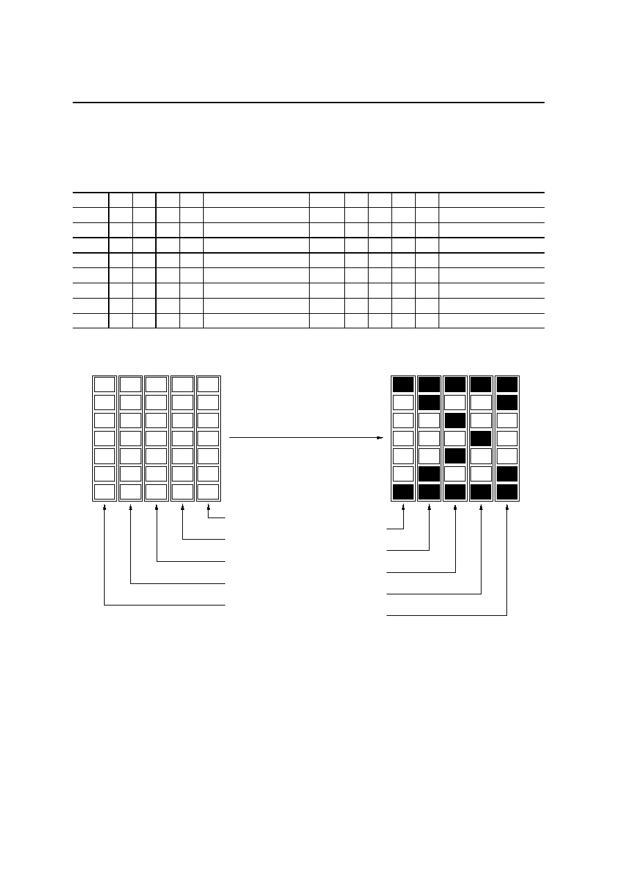
Positional Relationship Between SEGn and ADn (one digit)
C0
C0
SEGA1
C5
SEGA6
C10
SEGA11
C15
SEGA16
C20
SEGA21
C25
SEGA26
C30
SEGA31
C1
SEGA2
C6
SEGA7
C11
SEGA12
C16
SEGA17
C21
SEGA22
C26
SEGA27
C31
SEGA32
C2
SEGA3
C7
SEGA8
C12
SEGA13
C17
SEGA18
C22
SEGA23
C27
SEGA28
C32
SEGA33
C3
SEGA4
C8
SEGA9
C13
SEGA14
C18
SEGA19
C23
SEGA24
C28
SEGA29
C33
SEGA34
C4
SEGA5
C9
SEGA10
C14
SEGA15
C19
SEGA20
C24
SEGA25
C29
SEGA30
C34
SEGA35
Corresponds to the 2nd byte of the ADRAM_A data write command.
Corresponds to the 6th byte of the CGRAM_A data write command.
Corresponds to the 5th byte of the CGRAM_A data write command.
ADA
Corresponds to the 4th byte of the CGRAM_A data write command.
Corresponds to the 3rd byte of the CGRAM_A data write command.
Corresponds to the 2nd byte of the CGRAM_A data write command.
C0
C0
SEGB1
C5
SEGB6
C10
SEGB11
C15
SEGB16
C20
SEGB21
C25
SEGB26
C30
SEGB31
C1
SEGB2
C6
SEGB7
C11
SEGB12
C16
SEGB17
C21
SEGB22
C26
SEGB27
C31
SEGB32
C2
SEGB3
C7
SEGB8
C12
SEGB13
C17
SEGB18
C22
SEGB23
C27
SEGB28
C32
SEGB33
C3
SEGB4
C8
SEGB9
C13
SEGB14
C18
SEGB19
C23
SEGB24
C28
SEGB29
C33
SEGB34
C4
SEGB5
C9
SEGB10
C14
SEGB15
C19
SEGB20
C24
SEGB25
C29
SEGB30
C34
SEGB35
Corresponds to the 2nd byte of the ADRAM_B data write command.
Corresponds to the 6th byte of the CGRAM_B data write command.
Corresponds to the 5th byte of the CGRAM_B data write command.
ADB
Corresponds to the 4th byte of the CGRAM_B data write command.
Corresponds to the 3rd byte of the CGRAM_B data write command.
Corresponds to the 2nd byte of the CGRAM_B data write command.
COMn
PEDL9204-02
OKI Semiconductor
ML9204-xx
15/41
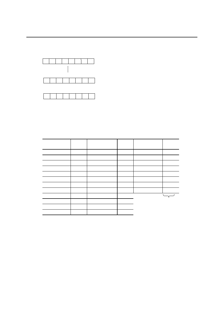
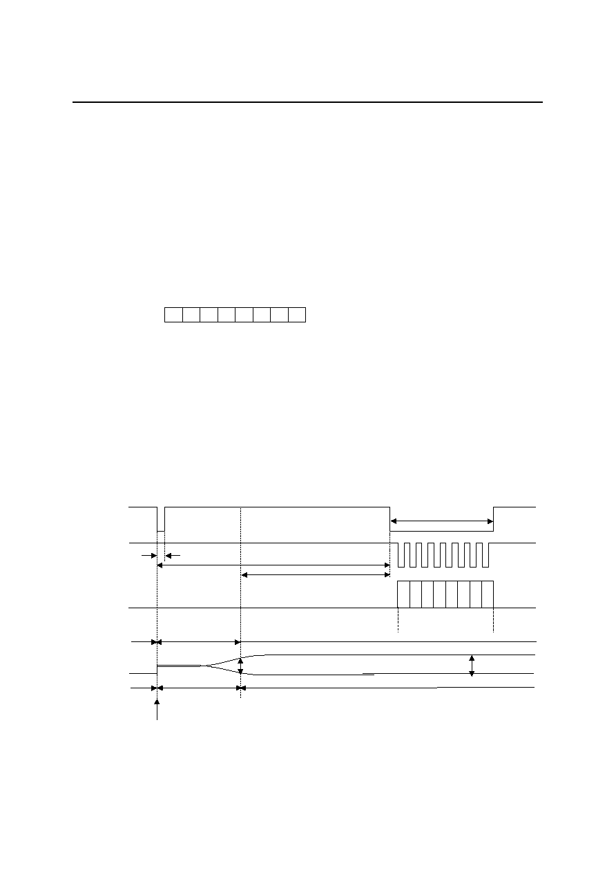
Data Transfer Method and Command Write Method
Display control command and data are written by an 8-bit serial transfer.
Write timing is shown in the figure below.
Setting the
CS pin to "Low" level enables a data transfer.
Data is 8 bits and is sequentially input into the DI/O pin from LSB (LSB first).
As shown in the figure below, data is read by the shift register at the rising edge of the shift clock, which is input
into the
CP pin. If 8-bit data is input, internal load signals are automatically generated and data is written to each
register and RAM.
Therefore it is not necessary to input load signals from the outside.
Setting the
CS pin to "High" disables data transfer. Data input from the point when the CS pin changes from
"High" to "Low" is recognized in 8-bit units.
* When data is written to RAM (DCRAM, ADRAM, CGRAM, GCRAM) continuously, addresses are internally
incremented automatically.
Therefore it is not necessary to specify the 1st byte to write RAM data for the 2nd and later bytes.
t
DOFF
LSB
CS
CP
MSB
1st byte
LSB
MSB
2nd byte
Command and address data
t
CSH
LSB
MSB
3rd byte
Character code data of the
next address
Character code data
When data is written
to DCRAM*
DA
B0
B1B2
B3
B4
B5
B6
B7
B0 B1B2 B3 B4 B5 B6 B7
B0 B1B2 B3
B4
B5
B6
B7

PEDL9204-02
OKI Semiconductor
ML9204-xx
16/41
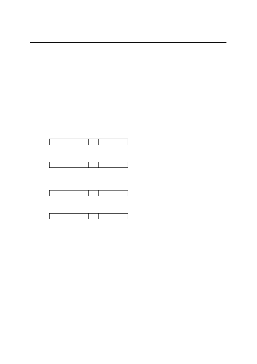
Data Outputting and Command Writing
In an operation to read key scan data, when
CS goes "Low" after Key Data Output Mode is entered, the DI/O pin
changes modes to OUTPUT and key data is output in synchronization with the rise of Shift Lock.
The waveforms to read key data are shown blow.
The DI/O pin enters the INPUT mode when the
CS pin is set to "High" after key data is output.
Keyscan stop
Data output (42-bit)
Key data output mode
CP
CS
t
CSH
LSB
MSB LSB
MSB
DI/O
B0 B1 B2 B3 B4 B5 B6 B7
B0 B1 B2 B3 B4 B5 B6 B7
VALID
Reset Function
Reset is executed when the
RESET pin is set to "L", (when turning power on, for example) and initializes all
functions.
Initial status is as follows.
∑ Address of each RAM ..................... address "00"H
∑ Data of each RAM .......................... All contents are undefined
∑ Display digit ................................... 24 digits
∑ Brightness adjustment..................... 0/1024
∑ All display lights ON or OFF.......... OFF mode
∑ Segment output............................... All segment outputs go "Low"
∑ AD output....................................... All AD outputs go "Low"
∑ ROW1 to 5...................................... All ROW outputs go "Low"
∑ INT................................................. INT goes "Low."
Be sure to execute the reset operation when turning power on and set again according to "Setting Flowchart"
after reset.

PEDL9204-02
OKI Semiconductor
ML9204-xx
17/41
Description of Commands and Functions
1,9. DCRAM data write
(Writes the character code of CGROM and CGRAM.)
DCRAM (Data Control RAM) has a 5-bit address to store character code of CGROM and CGRAM.
The character code specified by DCRAM is converted to a 5
◊
7 dot matrix character pattern via CGROM or
CGRAM.
(The DCRAM can store 24 characters.)
[Command format]
To specify the character code of CGROM and CGRAM continuously to the next address, specify only character
code as follows.
The addresses of DCRAM are automatically incremented. Specification of an address is unnecessary.
A character code setup of CGROM to 24-Digit and CGRAM is completion in the above work.
Furthermore, you have to specify the character codes of a dummy to be DCRAM and 18H-1FH to perform a
character code setup from DCRAM address 00H continuously.
(In order to carry out the increment of the address of DCRAM automatically and to set a DCRAM address to
00H.)
*
*
*
*
1
0
0
0/1
B0
B1
B2
B3 B4
B5
B6
B7
1st byte
(1st)
LSB
MSB
C0
C1
C2
C3 C4
C5
C6
C7
B0
B1
B2
B3 B4
B5
B6
B7
2nd byte
(2nd)
LSB
MSB
: Selects DCRAM data write mode
: Specifies character code of CGROM and CGRAM
(Written into DCRAM address 00H)
0: Select DCRAM_A
1: Select DCRAM_B
C0
C1
C2
C3 C4
C5
C6
C7
B0
B1
B2
B3 B4
B5
B6
B7
2nd byte
(3rd)
LSB
MSB
C0
C1
C2
C3 C4
C5
C6
C7
B0
B1
B2
B3 B4
B5
B6
B7
2nd byte
(4th)
LSB
MSB
: Specifies character code of CGROM and CGRAM
(Written into DCRAM address 01H)
: Specifies character code of CGROM and CGRAM
(Written into DCRAM address 02H)
B0
B1
B2
B3 B4
B5
B6
B7
2nd byte
(25th)
LSB
MSB
: Specifies character code of CGROM and CGRAM
(Written into DCRAM address 17H)
C0
C1
C2
C3 C4
C5
C6
C7

PEDL9204-02
OKI Semiconductor
ML9204-xx
18/41
C0 (LSB) to C7 (MSB): Character code of CGROM and CGRAM (8 bits: 256 characters)
*
:
Don't Care
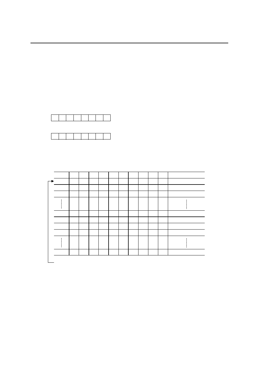
[COM positions and set DCRAM addresses]
DCRAM address
(HEX)
COM
DCRAM address
(HEX)
COM
DCRAM address
(HEX)
COM
00 COM1 0C
COM13
18
Dummy
01 COM2 0D
COM14
19
Dummy
02
COM3
0E
COM15
1A Dummy
03
COM4
0F
COM16
1B Dummy
04
COM5
10
COM17
1C Dummy
05
COM6
11
COM18
1D Dummy
06
COM7
12
COM19
1E Dummy
07
COM8
13
COM20
1F Dummy
08
COM9
14
COM21
09
COM10
15
COM22
0A
COM11
16
COM23
0B
COM12
17
COM24
CGROM of a dummy and the character code of CGRAM
are specified.
(It is not written in a DCRAM address.)
Character code of CGROM and CGRAM is specified.
(DCRAM address 00H are rewritten.)
8 times enforcement
C0
C1
C2
C3
C4
C5
C6
C7
B0
B1
B2
B3
B4
B5
B6
B7
2nd byte
(26th)
LSB
MSB
C0
C1
C2
C3
C4
C5
C6
C7
B0
B1
B2
B3
B4
B5
B6
B7
2nd byte
(33th)
LSB
MSB
:
:
B0
B1
B2
B3
B4
B5
B6
B7
2nd byte
LSB
MSB
:
C0
C1
C2
C3
C4
C5
C6
C7
(34th)
CGROM of a dummy and the character code of CGRAM
are specified.
(It is not written in a DCRAM address.)
Dummy is put in to set up a DCRAM
address from 00H continuously.
PEDL9204-02
OKI Semiconductor
ML9204-xx
19/41
2,A. CGRAM data write
(CGRAM writes character pattern data.)
CGRAM (Character Generator RAM) has a 4-bit address to store 5x 7 dot matrix character patterns.
A character pattern stored in CGRAM can be displayed by specifying the character code (address) by
DCROM.
The address of CGRAM is assigned to 00H to 0FH. (All the other addresses are the CGROM addresses.)
(The CGRAM can store 16 types of character patterns.)
[Command format]
To specify character pattern data continuously to the next address, specify only character pattern data as follows.
The addresses of CGRAM are automatically incremented. Specification of an address is unnecessary.
The 2nd to 6th byte (character pattern data) are regarded as one data item, so 200 ns is sufficient for t
DOFF
time
between bytes.
C0
C5
C10
C15
C20
C25
C30
*
B0
B1
B2
B3 B4
B5
B6
B7
2nd byte
(2nd)
LSB
MSB
: Specifies 1st column data
(Rewritten into CGRAM address 00H)
C1
C6
C11
C16
C21
C26
C31
*
B0
B1
B2
B3 B4
B5
B6
B7
3rd byte
(3rd)
LSB
MSB
: Specifies 2nd column data
(Rewritten into CGRAM address 00H)
0
0
0
0
0
1
0
0/1
B0
B1
B2
B3 B4
B5
B6
B7
1st byte
(1st)
LSB
MSB
: Selects CGRAM data write mode
C2
C7
C12
C17
C22
C27
C32
*
B0
B1
B2
B3 B4
B5
B6
B7
4th byte
(4th)
LSB
MSB
: Specifies 3rd column data
(Rewritten into CGRAM address 00H)
C3
C8
C13
C18
C23
C28
C33
*
B0
B1
B2
B3 B4
B5
B6
B7
5th byte
(5th)
LSB
MSB
: Specifies 4th column data
(Rewritten into CGRAM address 00H)
C4
C9
C14
C19
C24
C29
C34
*
B0
B1
B2
B3 B4
B5
B6
B7
6th byte
(6th)
LSB
MSB
: Specifies 5th column data
(Rewritten into CGRAM address 00H)
0: Select CGRAM_A
1: Select CGRAM_B
PEDL9204-02
OKI Semiconductor
ML9204-xx
20/41
X0 (LSB) to X3 (MSB) : CGRAM addresses (4 bits: 16 characters)
C0 (LSB) to C34 (MSB) : Character pattern data (35 bits: 35 outputs per digit)
* : Don't care
C0
C5
C10
C15C20
C25
C30
*
B0
B1
B2
B3 B4
B5
B6
B7
2nd byte
(7th)
LSB
MSB
: Specifies 1st column data
(Rewritten into CGRAM address 01H)
C4
C9
C14
C19C24
C29
C34
*
B0
B1
B2
B3 B4
B5
B6
B7
6th byte
(11th)
LSB
MSB
: Specifies 5th column data
(Rewritten into CGRAM address 01H)
C0
C5
C10
C15C20
C25
C30
*
B0
B1
B2
B3 B4
B5
B6
B7
2nd byte
(12th)
LSB
MSB
: Specifies 1st column data
(Rewritten into CGRAM address 02H)
C4
C9
C14
C19C24
C29
C34
*
B0
B1
B2
B3 B4
B5
B6
B7
6th byte
(16th)
LSB
MSB
: Specifies 5th column data
(Rewritten into CGRAM address 02H)
C0
C5
C10
C15C20
C25
C30
*
B0
B1
B2
B3 B4
B5
B6
B7
2nd byte
(77th)
LSB
MSB
: Specifies 1st column data
(Rewritten into CGRAM address 0FH)
C4
C9
C14
C19C24
C29
C34
*
B0
B1
B2
B3 B4
B5
B6
B7
6th byte
(81th)
LSB
MSB
: Specifies 5th column data
(Rewritten into CGRAM address 0FH)
C0
C5
C10
C15C20
C25
C30
*
B0
B1
B2
B3 B4
B5
B6
B7
2nd byte
(82th)
LSB
MSB
: Specifies 1st column data
(Rewritten into CGRAM address 00H)
C4
C9
C14
C19C24
C29
C34
*
B0
B1
B2
B3 B4
B5
B6
B7
6th byte
(86th)
LSB
MSB
: Specifies 5th column data
(Rewritten into CGRAM address 00H)
PEDL9204-02
OKI Semiconductor
ML9204-xx
21/41
[CGROM addresses and set CGRAM addresses]
Refer to ROM code tables.
HEX X0 X1 X2 X3
CGROM
address
HEX
X0
X1
X2
X3
CGROM
address
00 0 0 0 0 RAM00
(00000000B)
08 0
0
0
1
RAM08
(00001000B)
01 1 0 0 0 RAM01
(00000001B)
09 1
0
0
1
RAM09
(00001001B)
02 0 1 0 0 RAM02
(00000010B)
0A 0
1
0
1
RAM0A
(00001010B)
03 1 1 0 0 RAM03
(00000011B)
0B 1
1
0
1
RAM0B
(00001011B)
04 0 0 1 0 RAM04
(00000100B)
0C 0
0
1
1
RAM0C
(00001100B)
05 1 0 1 0 RAM05
(00000101B)
0D 1
0
1
1
RAM0D
(00001101B)
06 0 1 1 0 RAM06
(00000110B)
0E 0
1
1
1
RAM0E
(00001110B)
07 1 1 1 0 RAM07
(00000111B)
0F 1
1
1
1
RAM0F
(00001111B)
Positional relationship between the output area of CGRAM
Note: CGROM_A and CGROM_B (Character Generator ROM A, B) have an 8-bit address to generate
5 x 7
dot matrix character patterns.
Each of CGROM_A and CGROM_B can store 240 types of character patterns.
The contents of CGROM_A and CGROM_B can be set separately.
General-purpose code -01 is available (see ROM code tables) and custom codes are provided
on customer's request.
C0
SEGn1
C5
SEGn6
C10
SEGn11
C15
SEGn16
C20
SEGn21
C25
SEGn26
C30
SEGn31
C1
SEGn2
C6
SEGn7
C11
SEGn12
C16
SEGn17
C21
SEGn22
C26
SEGn27
C31
SEGn32
C2
SEGn3
C7
SEGn8
C12
SEGn13
C17
SEGn18
C22
SEGn23
C27
SEGn28
C32
SEGn33
C3
SEGn4
C8
SEGn9
C13
SEGn14
C18
SEGn19
C23
SEGn24
C28
SEGn29
C33
SEGn34
C4
SEGn5
C9
SEGn10
C14
SEGn15
C19
SEGn20
C24
SEGn25
C29
SEGn30
C34
SEGn35
Area that corresponds to 2nd byte (1st column)
(Input 1000001*B)
Area that corresponds to 3rd byte (2nd column)
(Input 1010101*B)
Area that corresponds to 4th byte (3rd column)
(Input 1001001*B)
Area that corresponds to 5th byte (4th column)
(Input 1100011*B)
Area that corresponds to 6th byte (5th column)
(Input 1100011*B)
C5
SEGn6
C10
SEGn11
C15
SEGn16
C20
SEGn21
C25
SEGn26
C11
SEGn12
C16
SEGn17
C21
SEGn22
C7
SEGn8
C17
SEGn18
C27
SEGn28
C8
SEGn9
C13
SEGn14
C23
SEGn24
C28
SEGn29
C14
SEGn15
C19
SEGn20
C24
SEGn25

PEDL9204-02
OKI Semiconductor
ML9204-xx
22/41
3,B. ADRAM data write
(ADRAM writes symbol data)
ADRAM (Additional Data RAM) has a 1-bit address to store symbol data.
Symbol data specified by ADRAM is directly output without CGROM and CGRAM.
(The ADRAM can store 1 type of symbol patterns for each digit.)
The terminal to which the contents of ADRAM are output can be used as a cursor.
[Command format]
To specify symbol data continuously to the next address, specify only character data as follows.
The address of ADRAM is automatically incremented. Specification of addresses is unnecessary.
A character code setup of 24-Digit is completion in the above work.
Furthermore, you have to specify the character codes of a dummy to be ADRAM and 18H-1FH to perform a
character code setup from ADRAM address 00H continuously.
(In order to carry out the increment of the address of ADRAM automatically and to set a ADRAM address to
00H.)
C0
*
*
*
*
*
*
*
B0
B1
B2
B3 B4
B5
B6
B7
2nd byte
(2nd)
LSB
MSB
: Sets symbol data
(Written into ADRAM address 00H)
*
*
*
*
1
1
0
0/1
B0
B1
B2
B3 B4
B5
B6
B7
1st byte
(1st)
LSB
MSB
: Selects ADRAM data write mode
0: Select ADRAM_A
1: Select ADRAM_B
C0
*
*
*
*
*
*
*
B0
B1
B2
B3 B4
B5
B6
B7
2nd byte
(3rd)
LSB
MSB
: Sets symbol data
(Written into ADRAM address 01H)
C0
*
*
*
*
*
*
*
B0
B1
B2
B3 B4
B5
B6
B7
2nd byte
(4th)
LSB
MSB
: Sets symbol data
(Written into ADRAM address 02H)
C0
*
*
*
*
*
*
*
B0
B1
B2
B3 B4
B5
B6
B7
2nd byte
(25th)
LSB
MSB
: Sets symbol data
(Written into ADRAM address 17H)
PEDL9204-02
OKI Semiconductor
ML9204-xx
23/41
C0 : Symbol data (1 bit: 1-symbol data per digit)
* : Don't care
[COM positions and ADRAM addresses]
ADRAM address
(HEX)
COM
ADRAM address
(HEX)
COM
ADRAM address
(HEX)
COM
00 COM1 0C COM13
18 Dammy
01 COM2 0D COM14
19 Dammy
02
COM3
0E
COM15
1A Dammy
03
COM4
0F
COM16
1B Dammy
04
COM5
10
COM17
1C Dammy
05
COM6
11
COM18
1D Dammy
06
COM7
12
COM19
1E Dammy
07
COM8
13
COM20
1F Dammy
08
COM9
14
COM21
09
COM10
15
COM22
0A
COM11
16
COM23
0B
COM12
17
COM24
C0
*
*
*
*
*
*
*
B0
B1
B2
B3 B4
B5
B6
B7
2nd byte
(26th)
LSB
MSB
: The sign data of a dummy is specified.
(It is not written in an ADRAM address.)
C0
*
*
*
*
*
*
*
B0
B1
B2
B3 B4
B5
B6
B7
2nd byte
(33th)
LSB
MSB
:
C0
*
*
*
*
*
*
*
B0
B1
B2
B3 B4
B5
B6
B7
2nd byte
(34th)
LSB
MSB
:
The sign data of a dummy is specified.
(It is not written in an ADRAM address.)
The sign data of a dummy is specified.
(ADRAM address 00H are rewritten.)
Dummy is put in to set up a ADRAM
address from 00H continuously.
PEDL9204-02
OKI Semiconductor
ML9204-xx
24/41
4. GCRAM data write
(writes data by the number of COM outputs for digits)
GCRAM (Grid Control RAM) has a 5-bit address to control the number of COM outputs for digits.
GCRAM outputs specified data directly to COMn, allowing COM outputs to be controlled arbitrarily.
It is also possible to supply a large current by connecting a plurality of COMs outside the ML9204.
For example, when COM23 and COM24 are connected, the ML9204 has 23 display digits. In this case, the user
specifies "23" as the number of display digits.
Write grid data at GCRAM addresses 00H and later.
Carry out this mode before putting-out-lights mode release.
Refer to a "setting operation flow chart" about the details of a setup.
Write COM data"0" in the GCRAM address which is not used for incorrect display prevention.
[Command format]
LSB
MSB
B0 B1 B2
B3 B4 B5 B6
B7
1st byte
*
*
*
*
0
0
1
0
: Selects a GCRAM data write mode.
(1st)
LSB
MSB
B0 B1 B2
B3 B4 B5 B6
B7
2nd
byte
C0 C1 C2
C3 C4 C5 C6
C7
: Specifies
COM
data.
(2nd)
(Written
into
GCRAM
address
00H)
LSB
MSB
B0 B1 B2
B3 B4 B5 B6
B7
3rd byte C8 C9 C10 C11 C12 C13 C14 C15 : Specifies COM data.
(3rd)
(Written
into
GCRAM
address
00H)
LSB
MSB
B0 B1 B2
B3 B4 B5 B6
B7
4th byte C16 C17 C18 C19 C20 C21 C22 C23 : Specifies COM data.
(4th)
(Written
into
GCRAM
address
00H)
C0 (LSB) to C23 (MSB): Grid control data (24 bits)
*: Don't Care
Note: To specify additional grid control data, specify the grid control data as shown below. The GCRAM
addresses are automatically incremented.
The second byte to the fourth byte (for grid data) are treated as a single piece of element and the
byte-byte t
DOFF
can be 200 ns.

PEDL9204-02
OKI Semiconductor
ML9204-xx
25/41
LSB
MSB
B0 B1 B2
B3 B4 B5 B6
B7
2nd
byte C0 C1 C2
C3 C4 C5 C6
C7
: Specifies
COM
data.
(5th)
(Written
into
GCRAM
address
01H)
LSB
MSB
B0 B1 B2
B3 B4 B5 B6
B7
4th byte C16 C17 C18 C19 C20 C21 C22 C23 : Specifies COM data.
(7th)
(Written
into
GCRAM
address
01H)
LSB
MSB
B0 B1 B2
B3 B4 B5 B6
B7
2nd
byte C0 C1 C2
C3 C4 C5 C6
C7
: Specifies
COM
data.
(71st)
(Written
into
GCRAM
address
17H)
LSB
MSB
B0 B1 B2
B3 B4 B5 B6
B7
4th byte C16 C17 C18 C19 C20 C21 C22 C23 : Specifies COM data.
(73rd)
(Written
into
GCRAM
address
17H)
With the above operations, COM data of up to 24 digits are set. To set other COM data at GCRAM addresses
00H and later, specify dummy symbol data at GCRAM addresses 18H to 1FH (to automatically increment the
GCRAM address and set the GCRAM address to 00H).
[GCRAM addresses (digit positions) and COM positions]
GCRAM
address
(HEX)
1(00) 2(01) 3(02)
22(15)
23(16) 24(17)
COM1 C0
C1 C2
C21
C22 C23
COM2 C0
C1 C2
C21
C22 C23
COM3 C0
C1 C2
C21
C22 C23
COM4 C0
C1 C2
C21
C22 C23
COM5 C0
C1 C2
C21
C22 C23
COM20 C0 C1 C2
C21 C22 C23
COM21 C0 C1 C2
C21 C22 C23
COM22 C0 C1 C2
C21 C22 C23
COM23 C0 C1 C2
C21 C22 C23
COM24 C0 C1 C2
∑ ∑ ∑ ∑ ∑
C21 C22 C23

PEDL9204-02
OKI Semiconductor
ML9204-xx
26/41
[GCRAM output example]
1. When 4-digit of the 9-digit display requires an output current of 40 mA
<Setup>
Number setup of display beams: 9-digit
GCRAM setup:4-digit of COM4 and COM5
* Write "0" also in the beam which is not used.
GCRAM
address
(HEX)
1(00)
2(01) 3(02) 4(03) 5(04)
6(05)
7(08)
8(07)
9(08)
11(09)
11(0A)
......
23(16) 24(17)
COM1
1 0 0 0 0 0 0 0 0 0 0
0 0
COM2
0 1 0 0 0 0 0 0 0 0 0
0 0
COM3
0 0 1 0 0 0 0 0 0 0 0
0 0
COM4
0 0 0 1 0 0 0 0 0 0 0
0 0
COM5
0 0 0 1 0 0 0 0 0 0 0
0 0
COM6
0 0 0 0 1 0 0 0 0 0 0
0 0
COM7
0 0 0 0 0 1 0 0 0 0 0
0 0
COM8
0 0 0 0 0 0 1 0 0 0 0
0 0
COM9
0 0 0 0 0 0 0 1 0 0 0
0 0
COM10
0 0 0 0 0 0 0 0 1 0 0
......
0 0
COM1
COM2
COM3
COM4
COM5
D
s
i
p
l
a
y t
ube
COM1
COM2
COM3
COM4
COM5
COM6
Strap
COM6
COM7
COM8
COM9
COM7
COM8
COM9
COM10
COM10
GRID1
GRID2
GRID3
GRID4
GRID5
GRID6
GRID7
GRID8
GRID9
* Strapping COM4 and COM5 brings display digits to 9 digits, and a current of 50 mA can be supplied.
1 Cycle

PEDL9204-02
OKI Semiconductor
ML9204-xx
27/41
2. When only one digit of the 22-digit display requires an output current of 60 mA
<Setup>
Number setup of display beams:22-digit
GCRAM setup:1-digit of COM1 and COM23 and COM24
* Write "0" also in the beam which is not used.
GCRAM
address
(HEX)
1(00)
2(01) 3(02) 4(03) 5(04)
6(05)
7(08) 8(07)
9(08) 11(09)
......
22(15)
23(16) 24(17)
COM1
1 0 0 0 0 0 0 0 0 0
0 0 0
COM2
0 1 0 0 0 0 0 0 0 0
0 0 0
COM3
0 0 1 0 0 0 0 0 0 0
0 0 0
COM22
0 0 0 0 0 0 0 0 0 0
1 0 0
COM23
1 0 0 0 0 0 0 0 0 0
0 0 0
COM24
1 0 0 0 0 0 0 0 0 0
......
0 0 0
* Strapping COM1, COM23 and COM24 brings display digits to 22 digits, and a current of 75 mA can be
supplied.
COM1
COM2
COM3
Strap
COM1
COM2
COM3
COM23
COM24
COM24
COM23
COM22
COM22
GRID1
GRID2
GRID3
GRID22
1 Cycle
Dis
p
l
a
y
t
ube
PEDL9204-02
OKI Semiconductor
ML9204-xx
28/41
5. Display duty set
(writes display duty value to duty cycle register)
Display duty adjusts brightness in 1024 stages using 10-bit data.
When power is turned on or when the
RESET signal is input, the duty cycle register value is "0". Always
execute this instruction before turning the display on, then set a desired duty value.
[Command format]
D0 (LSB) to D9 (MSB) : Display duty data (10 bits: 1024 stages)
* : Don't care
[Relation between setup data and controlled COM duty]
HEX D0
D1 D2 D3 D4
D5
D6
D7
D8
D9
COM
duty
000 0 0 0 0 0
0
0
0
0
0
0/1024
001 1 0 0 0 0
0
0
0
0
0
1/1024
002 0 1 0 0 0
0
0
0
0
0
2/1024
3BE 0 1 1 1 1
1
0
1
1
1
958/1024
3BF 1 1 1 1 1
1
0
1
1
1
959/1024
3C0 0 0 0 0 0
0
1
1
1
1
960/1024
3C1 1 0 0 0 0
0
1
1
1
1
960/1024
3FF 1 1 1 1 1
1
1
1
1
1
960/1024
The state when power is turned on or when
RESET
signal is input.
D0
D1
*
*
1
0
1
0
B0
B1
B2
B3 B4
B5
B6
B7
1st byte
LSB
MSB
: Selects display duty set mode and sets duty value (lower 2 bits)
D2
D3
D4
D5 D6
D7
D8
D9
B0
B1
B2
B3 B4
B5
B6
B7
2nd byte
(2nd)
LSB
MSB
: sets duty value (upper 8 bits)
(1st)

PEDL9204-02
OKI Semiconductor
ML9204-xx
29/41
6. Number of digits set
(writes the number of display digits to the display digit register)
The number of digits set can display 9 to 24 digits using 4-bit data.
When power is turned on or when a
RESET signal is input, the number of digit register value is "0". Always
execute this instruction to change the number of digits before turning the display on.
[Command format]
K0 (LSB) to K3 (MSB) : Number of digit data (4 bits: 24 digits)
* : Don't care
[Relation between setup data and controlled COM]
* When the number of COM is one at 1 digit
HEX K0 K1 K2
K3
Number of digits of
COM
HEX
K0
K1
K2
K3
Number of digits of
COM
0
0
0
0
0
1-24(COM1 to 24)
0
0
0
0
1
1-16(COM1 to 16)
1
1
0
0
0
1-9(COM1 to 9)
1
1
0
0
1
1-17(COM1 to 17)
2
0
1
0
0
1-10(COM1 to 10)
2
0
1
0
1
1-18(COM1 to 18)
3
1
1
0
0
1-11(COM1 to 11)
3
1
1
0
1
1-19(COM1 to 19)
4
0
0
1
0
1-12(COM1 to 12)
4
0
0
1
1
1-20(COM1 to 20)
5
1
0
1
0
1-13(COM1 to 13)
5
1
0
1
1
1-21(COM1 to 21)
6
0
1
1
0
1-14(COM1 to 14)
6
0
1
1
1
1-22(COM1 to 22)
7
1
1
1
0
1-15(COM1 to 15)
7
1
1
1
1
1-23(COM1 to 23)
The state when power is turned on or when
RESET
signal is input.
K0 K1 K2 K3 0
1
1
0
B0 B1 B2 B3 B4 B5 B6 B7
1st byte
LSB
MSB
: selects the number of digit set mode and specifies
the number of digit value

PEDL9204-02
OKI Semiconductor
ML9204-xx
30/41
7. All display lights ON/OFF set
(turns all display lights ON or OFF)
All display lights ON is used primarily for display testing.
All display lights OFF is primarily used for display blink and to prevent malfunction when power is turned on.
[Command format]
L, H : Display operation data
* : Don't care
[Set data and display state of SEG and AD]
L
H
Display state of SEG and AD
0 0 Normal
display
1
0
Sets all outputs to Low
0
1
Sets all outputs to High
1
1
Sets all outputs to High
* Priority is given to an all-points light command.
L
H
*
*
1
1
1
0
B0
B1
B2
B3
B4
B5 B6 B7
1st byte
LSB
MSB
: Selects all display lights ON or OFF mode

PEDL9204-02
OKI Semiconductor
ML9204-xx
31/41
C. Key scan stop
This command stops key scanning and makes ROW1 to ROW5 outputs "Low" and the INT output "Low".
[Command format]
LSB
MSB
B0 B1 B2
B3 B4 B5 B6
B7
1st byte
*
*
*
*
0
0
1
1
: stops key scanning.
*: Don't Care
D. Key data output
This command puts the pin in the output mode and causes the pin to output the scanned switch data.
The DI/O pin outputs 42-bit switch data at the rise of a clock.
When the
CS pin goes high, the DI/O pin enters the output mode.
"R1, R2, R3 = 0" means turning a control knob clockwise.
"R1, R2, R3 = 1" means turning a control knob counterclockwise.
Contact count bits are Q11(LSB) to Q13(MSB), Q21(LSB) to Q23(MSB), and Q31(LSB) to Q33(MSB).
[Command format]
LSB
MSB
B0 B1 B2
B3 B4 B5 B6
B7
1st byte
*
*
*
*
1
0
1
1
: outputs key data.
*: Don't Care
[COL input and ROW output key-switch matrix]
COL1
S11
S21
S31
S41
S12
S22
S32
S42
S13
S23
S33
S43
S14
S24
S34
S44
S51
S52
S53
S54
S55
COL2
COL3
COL4
S15
S25
S35
S45
COL5
ROW1
ROW2
ROW3
ROW4
ROW5
S16
S26
S36
S46
COL6
S56

PEDL9204-02
OKI Semiconductor
ML9204-xx
32/41
[Output Data Format]
Output data: 42 bits
5
◊
6 push switch data: 30 bits
Encoder switch data: 12 bits
Bit
1 2 3 4 5 6 7 8 9 10 11 12
Output Data
S11
S12
S13
S14
S15
S16
S21
S22
S23
S24
S25
S26
Bit
13 14 15 16 17 18 19 20 21 22 23 24
Output Data
S31
S32
S33
S34
S35
S36
S41
S42
S43
S44
S45
S46
Bit
25 26 27 28 29 30 31 32 33 34 35 36
Output Data
S51
S52
S53
S54
S55
S56
R1
Q11
Q12
Q13
R2
Q21
Bit
37 38 39 40 41 42
Output Data
Q22
Q23
R3
Q31
Q32
Q33
Sij: i = ROW1 to 5; j = COL1 to 6
Sij = 1: switch ON
Sij = 0: switch OFF
PEDL9204-02
OKI Semiconductor
ML9204-xx
33/41
Keyscan
Keyscanning is started only when depression or release of any key is detected in order to minimize noise caused
by scanning signal. Then, keyscanning is continued until the keyscan stop mode is sent from a microcomputer.
The INT pin goes to the high level at the completion of 1-cycle scanning after the keyscan start, so the (high
level) signal sent from the INT pin can be used as an interrupt signal.
[Keyscan Timing and Cycles]
Depress/Release
keyscan stop
1 keyscan cycle
ROW1
ROW2
ROW3
ROW4
ROW5
INT
Keyscanning cannot be stopped by selecting the keyscan stop mode only once if:
- keyscanning is started after depression or release of any key is detected, and then
- a key is depressed or released again before the keyscan stop mode is selected.
To stop keyscanning, it is required to select the keyscan stop mode once again.
KS
KS
KS
Depress
Release
Keyscan
Depress
Keyscan
INT
CS
KS: Keyscan stop mode
PEDL9204-02
OKI Semiconductor
ML9204-xx
34/41
The rotary encoder switch function
As Figure 1 shows, the rotary encoder switch circuit is consisted of Phase detection, Interrupt generation,
Up/down counter, Direction latch and Parallel-in serial-out shift register.
The Rotary Encoder Switch Circuit
1. Phase detection
1-1. Clockwise rotation
The input A and B have a chattering absorption circuit of 256
µ
s period. When signal A and B input as shown
below, the phase detection circuit outputs UP signal after the chattering absorption period. At this time, the
output INT also goes to high level, so this signal can be used as an interrupt. The INT stays High level until the
keyscan stop mode is selected.
UP (internal)
B
A
INT
chattering absorption time
The Input and Output Timing in the Case of Clockwise Rotation
Phase Detection
UP DOWN
B
Q3 Q2 Q1
A
UP/DOWN Counter
P-in/S-out Shift Register
R1
Direction Latch
Interrupt
Generation
for INT
Output data
PEDL9204-02
OKI Semiconductor
ML9204-xx
35/41
1-2. Counterclockwise rotation
When signal A and B input as shown below, the phase detection circuit outputs Down signal after the chattering
absorption period. At this time, the output INT also goes to High level. The INT stays High level until the
keyscan stop mode is selected.
DOWN (internal)
B
A
INT
chattering absorption time
The Input and Output Timing in the Case of Counterclockwise Rotation
2. UP/DOWN COUNTER
When the UP/DOWN COUNTER is input UP, it counts up and when it is input DOWN, it counts down.
But if the UP/DOWN COUNTER is incremented beyond "111", it stays "111".
B
Q1, Q2, Q3
A
100 010 110
001
101 011
111 111
Counter Overflow
3. Direction latch
When the Direction latch is input DOWN the output R1 goes "1". But if the UP pulse is input and the count
value changes to a positive value, the output R1 goes to "0".
100
Q1, Q2, Q3
100 100
B
A
010
000
010
R1
Direction Latch
PEDL9204-02
OKI Semiconductor
ML9204-xx
36/41
F. Standby mode set
(Display all switched off and an oscillation stopped)
Standby mode realizes low power consumption of VDD, VSEG, and VCOM by all switching off a display,
stopping an oscillation of an external (COM is fixed to Low) oscillation child, and stopping internal operation
completely. All display lights OFF is primarily used for display blink and to prevent malfunction when power is
turned on.
* If a RESET signal is inputted during standby mode execution, standby mode is canceled, and keep in mind it
that all states will be initialized.
[Command format]
* : Don't care
[Release standby mode]
Release in standby mode is performed in falling of CS. (An oscillation child's oscillation is started)
Data input will become possible if an oscillation is stabilized. (Please return brought-down CS high-level before
data input)
When you display after standby mode release since it is all putting out lights although the setting state is held,
please cancel all putting-out-lights modes (in usual mode).
* Please do not input a shift clock into CP until an oscillation is stabilized. (Data will be given)
tRSON (oscillation standup time) changes with oscillation children who use it. Please make reference an
oscillation child's data to be used.
*
*
*
*
1
1
1
1
1
B0
B1
B2
B3
B4
B5 B6 B7
1st byte
LSB
MSB
: Standby mode is specified.
OSC0
0.9Vp-p
Vp-p
t
RSON
Set it as 200nsec.
CS
CP
LSB
MSB
1st byte
* May not place the section.
DA
B0 B1B2 B3
B4
B5
B6
B7
Data input
Oscillation stop state
Standby release,
Standby section
Usually, a state of operation
(all putting-out-lights states)
Standby state
Oscillation unstable state
(oscillation standup time)
Oscillation stable state
Oscillation start
PEDL9204-02
OKI Semiconductor
ML9204-xx
37/41
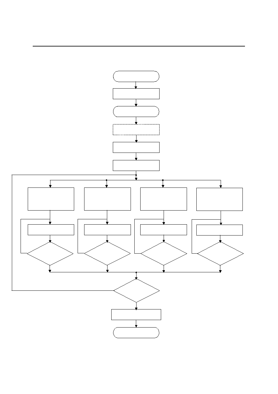
SETTING FLOWCHART
(Power applying included)
Apply V
SEG
/V
COM
All display lights OFF
Number of digits setting
Display duty setting
CGRAM_A or B
Data write mode
(with address setting)
CGRAM_A or B
Character code
Another RAM to
be set?
Releases all display lights
OFF mode
ADRAM_A or B
Data write mode
ADRAM_A or B
Character code
DCRAM_A or B
Data write mode
DCRAM_A or B
Character code
DCRAM
Is character code
write ended?
Select a RAM to be used
Status of all outputs by
RESET
Display operation mode
NO
NO
NO
YES
YES
YES
YES
End of setting
Apply V
DD
NO
Address is automatically
incremented
Address is automatically
incremented
Address is automatically
incremented
CGRAM
Is character code
write ended?
ADRAM
Is character code
write ended?
RESET
execution
GCRAM
Data write mode
GCRAM code
NO
YES
Address is automatically
incremented
GCRAM
write ended?

PEDL9204-02
OKI Semiconductor
ML9204-xx
38/41
POWER-OFF FLOWCHART
APPLICATION CIRCUIT
*1 The V
SEG
and V
COM
voltages depend on the fluorescent display tube used. Adjust the value of the
constants R and ZD to the V
SEG
and V
COM
voltages used.
*2 The wiring trace between the OSC0 pin and the resonator should be kept as short as possible, and
the GND traces should be provided along both sides of the wiring trace.
*3 Adjust the capacitance of the capacitor depending on the type of the oscillator used. (Refer to the
data of oscillator used.)
Display operation mode
Turn off V
DD
Turn off V
SEG
/V
COM
24
35
35
V
DD
MCU
V
DD
GND
Output port
2
R
ZD
V
SEG
/ V
COM
Crystal oscillation or
Ceramic oscillation
L-GND D-GND
OSC0 OSC1
5 x 7
dot matrix fluorescent display
ANODE
(SEGMENT)
ANODE
(SEGMENT)
GRID
(DIGIT)
ANODE
(SEGMENT)
V
SEG
ML9204-xx
COM1-24
SEGA1-A35
SEGB1-B35
RESET
V
DD
DI/O
CP
CS
ADA,ADB
V
COM
INT
*1
*2
*3
5x6Key matrix
and rotary switch
COL1
-
6
ROW1-5
B1-3
A1-3

PEDL9204-02
OKI Semiconductor
ML9204-xx
39/41
PACKAGE DIMENSIONS
QFP128-P-1420-0.50-K
Mirror finish
Package material
Epoxy resin
Lead frame material
42 alloy
Pin treatment
Solder plating (
5µm)
Package weight (g)
1.19 TYP.
5
Rev. No./Last Revised
4/Nov. 28, 1996
Notes for Mounting the Surface Mount Type Package
The surface mount type packages are very susceptible to heat in reflow mounting and humidity
absorbed in storage.
Therefore, before you perform reflow mounting, contact Oki's responsible sales person for the product
name, package name, pin number, package code and desired mounting conditions (reflow method,
temperature and times).
(Unit: mm)

PEDL9204-02
OKI Semiconductor
ML9204-xx
40/41
REVISION HISTORY
Page
Document No.
Date
Previous
Edition
Current
Edition
Description
PEDL9204-01
Jan. 8, 2003
≠
≠
Preliminary edition 1
PEDL9204-02
Oct. 12, 2004
4
4
Pin description added

PEDL9204-02
OKI Semiconductor
ML9204-xx
41/41
NOTICE
1. The information contained herein can change without notice owing to product and/or technical
improvements. Before using the product, please make sure that the information being referred to is
up-to-date.
2. The outline of action and examples for application circuits described herein have been chosen as an
explanation for the standard action and performance of the product. When planning to use the product,
please ensure that the external conditions are reflected in the actual circuit, assembly, and program designs.
3. When designing your product, please use our product below the specified maximum ratings and within the
specified operating ranges including, but not limited to, operating voltage, power dissipation, and operating
temperature.
4. Oki assumes no responsibility or liability whatsoever for any failure or unusual or unexpected operation
resulting from misuse, neglect, improper installation, repair, alteration or accident, improper handling, or
unusual physical or electrical stress including, but not limited to, exposure to parameters beyond the
specified maximum ratings or operation outside the specified operating range.
5. Neither indemnity against nor license of a third party's industrial and intellectual property right, etc. is
granted by us in connection with the use of the product and/or the information and drawings contained
herein. No responsibility is assumed by us for any infringement of a third party's right which may result
from the use thereof.
6. The products listed in this document are intended for use in general electronics equipment for commercial
applications (e.g., office automation, communication equipment, measurement equipment, consumer
electronics, etc.). These products are not, unless specifically authorized by Oki, authorized for use in any
system or application that requires special or enhanced quality and reliability characteristics nor in any
system or application where the failure of such system or application may result in the loss or damage of
property, or death or injury to humans.
Such applications include, but are not limited to, traffic and automotive equipment, safety devices,
aerospace equipment, nuclear power control, medical equipment, and life-support systems.
7. Certain products in this document may need government approval before they can be exported to particular
countries. The purchaser assumes the responsibility of determining the legality of export of these products
and will take appropriate and necessary steps at their own expense for these.
8. No part of the contents contained herein may be reprinted or reproduced without our prior permission.
Copyright 2004 Oki Electric Industry Co., Ltd.