ChipFind - документация

Электронный компонент: ML9207-XXGA

Скачать:  PDF   ZIP

Document Outline

OKI Semiconductor
FEDL9207-02
Issue Date: May 17, 2005
ML9207-xx
5
7 Dot Character
24-Digit Display Controller/Driver with Character RAM
1/35
GENERAL DESCRIPTION

The ML9207-xx is a dot matrix vacuum fluorescent display tube controller driver IC which displays characters,
numerics and symbols.
Dot matrix vacuum fluorescent display tube drive signals are generated by serial data sent from a micro-controller.
A display system is easily realized by internal ROM and RAM for character display.
The ML9207-xx has low power consumption since it is made by CMOS process technology.
-01 is available as a general-purpose code.
Custom codes are provided on customer's request.
FEATURES
Logic power supply (V
DD
)
: 3.3 V
10% or 5.0 V
10%
Fluorescent display tube drive power supply (V
DISP
) : 3.3 V
10% or 5.0 V
10%
Fluorescent display tube drive power supply (V
FL
) : 20 to 60 V
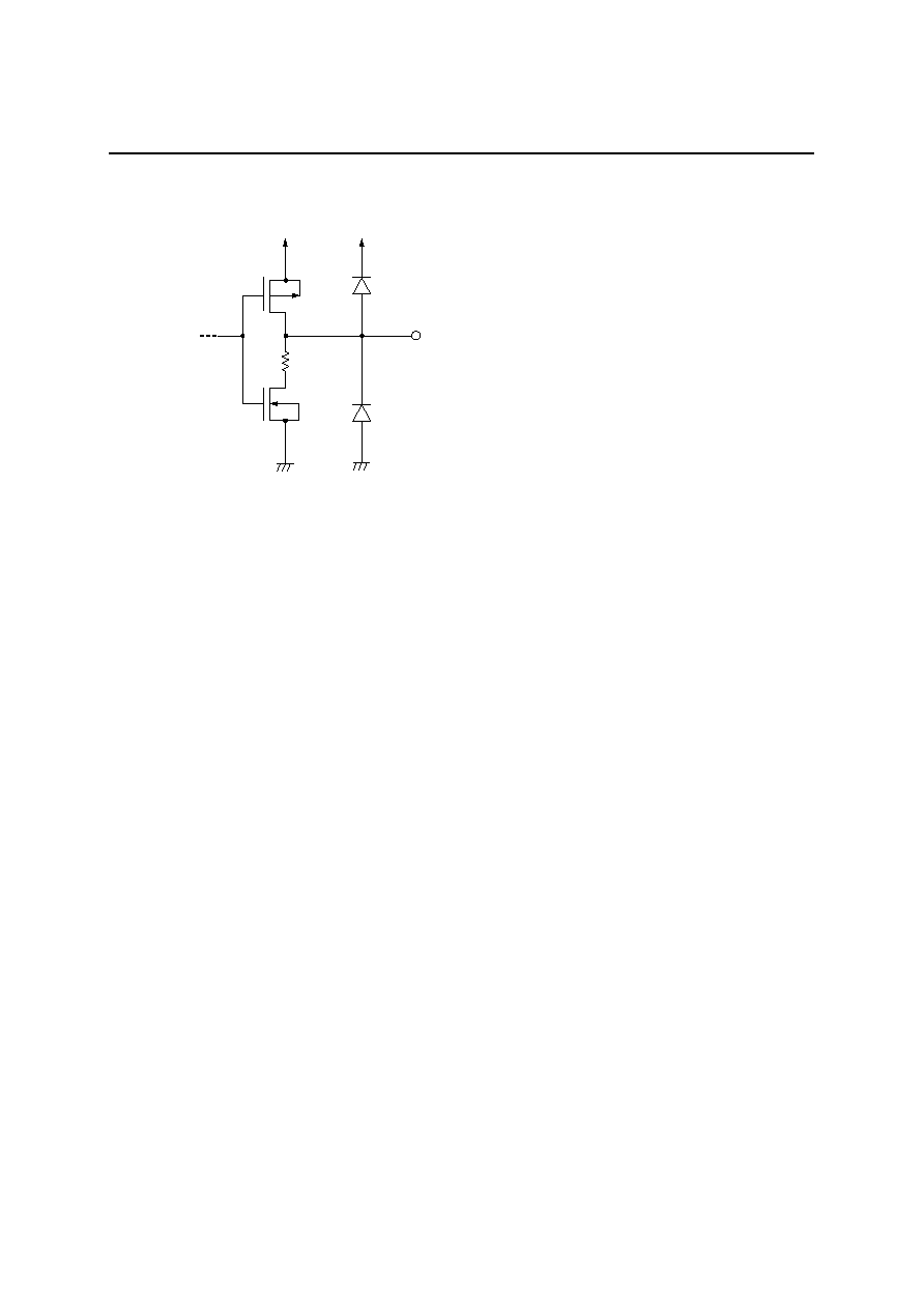
VFD driver output current
(VFD driver output can be connected directly to the fluorescent display tube. No pull-down resistor is
required.)
Segment driver (SEG1 to SEG35)
: 5.0 mA
(V
FL
= 60 V)
Segment driver (AD1 to AD4)
: 10.0 mA
(V
FL
= 60 V)
Grid driver (COM1 to COM24)
: 50.0 mA
(V
FL
= 60 V)
General output port output current
Output driver (P1 to P4)
:
1.0 mA (V
DD
= 3.3 V
10%)
2.0 mA (V
DD
= 5.0 V
10%)
Content of display
CGROM 5
7 dots
: 240 types (character data)
CGRAM 5
7 dots
: 16 types (character data)
ADRAM
24 (display digit)
4 bits (symbol data)
DCRAM
24 (display digit)
8 bits (register for character data display)
General output port
4 bits (static operation)
Display control function
Display digit
: 9 to 24 digits
Display duty (brightness adjustment) : 0/1024 to 960/1024
All lights ON/OFF
4 interfaces with microcontroller
: DA,
CS, CP, RESET
1-byte instruction execution (excluding data write to RAM and Display duty set)
Built-in oscillation circuit
Crystal oscillation or ceramic oscillation
Package
options:
80-pin QFP package (QFP80-P-1414-0.65-K) (Product name : ML9207-xxGP)
80-pin QFP package (QFP80-P-1420-0.80-BK) (Product name : ML9207-xxGA)
xx indicates the code number.
FEDL9207-02
OKI Semiconductor
ML9207-xx
2/35
BLOCK DIAGRAM
V
DD
GND
V
FL
RESET
DA
CP
CS
OSC0
OSC1
SEG1
SEG35
AD1
AD4
P1
P4
COM1
COM24
DCRAM
24w
8b
CGROM
CGRAM
16w
35b
ADRAM
24w
4b
8-bit
Shift
Register
Command
Decoder
Control
Circuit
Timing
Oscillator
Timing
Digit
Control
Duty
Control
Grid
Driver
Port
Driver
AD
Driver
Segment
Driver
Write
Address
Counter
Read
Address
Counter
Address
Selector
V
DISP
240w
35b
Generator1
Generator2
FEDL9207-02
OKI Semiconductor
ML9207-xx
3/35
SCHEMATIC DIAGRAM OF DRIVER OUTPUT CIRCUIT


V
FL
V
FL
V
DISP
OUTPUT
V
DISP
FEDL9207-02
OKI Semiconductor
ML9207-xx
4/35
PIN CONFIGURATION (TOP VIEW)

NC: No connection
80-Pin Plastic QFP
(QFP80-P-1414-0.65-K)
80
79
78
77
76
75
74
73
72
71
70
69
68
67
66
65
64
63
62
61
AD2
AD1
V
D
I
SP2
N
C
V
FL
2
P4
P
3
P2
P1
V
DD
D
A
C
P
C
S
R
ES
E
T
OS
C
1
OS
C
0
G
ND
V
FL
1
CO
M2
4
CO
M2
3
21
22
23
24
25
26
27
28
29
30
31
32
33
34
35
36
37
38
39
40
S
E
G
1
9
S
E
G
2
0
S
E
G
21
S
E
G
22
S
E
G
2
3
S
E
G
24
S
E
G
2
5
S
E
G
2
6
S
E
G
27
S
E
G
2
8
S
E
G
2
9
SEG
3
0
SEG
3
1
SEG
3
2
S
E
G3
3
S
E
G3
4
S
E
G3
5
V
D
I
SP1
CO
M1
CO
M2
60
59
58
57
56
55
54
53
52
51
50
49
48
47
46
45
44
43
42
41
COM22
COM21
COM20
COM19
COM18
COM17
COM16
COM15
COM14
COM13
COM12
COM11
COM10
COM9
COM8
COM7
COM6
COM5
COM4
COM3
1
2
3
4
5
6
7
8
9
10
11
12
13
14
15
16
17
18
19
20
AD3
AD4
SEG1
SEG2
SEG3
SEG4
SEG5
SEG6
SEG7
SEG8
SEG9
SEG10
SEG11
SEG12
SEG13
SEG14
SEG15
SEG16
SEG17
SEG18
FEDL9207-02
OKI Semiconductor
ML9207-xx
5/35
NC: No connection
80-Pin Plastic QFP
(QFP80-P-1420-0.80-BK)
COM1
41
COM2
42
COM3
43
COM4
44
COM5
45
COM6
46
COM7
47
COM8
48
COM9
49
COM10
50
COM11
51
COM12
52
COM13
53
COM14
54
COM15
55
COM16
56
COM17
57
COM18
58
COM19
59
COM20
60
COM21
61
COM22
62
COM23
63
COM24
64
V
D
I
SP1
40
S
E
G3
5
39
S
E
G3
4
38
S
E
G3
3
37
S
E
G3
2
36
S
E
G3
1
35
S
E
G3
0
34
S
E
G
2
9
33
SEG
2
8
32
SEG
2
7
31
S
E
G
2
6
30
S
E
G
2
5
29
S
E
G
24
28
S
E
G
2
3
27
S
E
G
22
26
S
E
G
21
25
24
23
22
21
20
19
18
17
16
15
14
13
12
11
10
9
8
7
6
5
4
3
2
1
SEG20
SEG19
SEG18
SEG17
SEG16
SEG15
SEG14
SEG13
SEG12
SEG11
SEG10
SEG9
SEG8
SEG7
SEG6
SEG5
SEG4
SEG3
SEG2
SEG1
AD4
AD3
AD2
AD1
65
66
67
68
69
70
71
72
73
74
75
76
77
78
79
80
V
FL
1
G
ND
OS
C
0
OS
C
1
R
ES
E
T
C
S
C
P
D
A
V
DD
P1
P2
P
3
P4
V
FL
2
N
C
V
D
I
SP2