
Semiconductor
This version: Sep. 2000
MS81V06160
Preliminary
(401,408-word
◊
16-bit) FIFO memory
1/18
GENERAL DESCRIPTION
The MS81V06160 is a 6Mb FIFO (First-In First-Out) memory designed for 401,408-words
◊
16-bit high-speed
asynchronous read/write operation.
The MS81V06160 is best suited for a field memory for digital TVs or LCD panels which require high-speed, large
memory , and is not designed for high end use in professional graphics systems, which require long term picture
storage and data storage.
The MS81V06160 is provided with independent control clocks to support asynchronous read and write operations.
Different clock rates are also supported, which allow alternate data rates between write and read data streams.
The first data read operation can be performed after 1600 ns + 4 cycles from read reset and the first data write
operation is enabled after 1600 ns + 4 cycles from write reset. Thereafter, the high-speed read/write operation is
possible every cycle time.
Additionally, a write mask function by IE pin and a read-data skipping function by OE pin implement image data
processing easily.
The MS81V06160 provides high speed FIFO (First-in First-out) operation without external refreshing:
MS81V06160 refreshes its DRAM storage cells automatically, so that it appears fully static to the users.
Moreover, fully static type memory cells and decoders for serial access enable the refresh free serial access
operation, so that serial read and/or write control clock can be halted high or low for any duration as long as the
power is on. Internal conflicts of memory access and refreshing operations are prevented by special arbitration
logic.
The MS81V06160's function is simple, and similar to a digital delay device whose delay-bit- length is easily set by
reset timing. The delay length and the number of read delay clocks between write and read, is determined by
externally controlled write and read reset timings. The MS81V06160 uses a thin and small 70-pin plastic TSOP.

Semiconductor
MS81V06160
2/18
FEATURES
∑
401,408 words
◊
16 bits
∑
Fast FIFO (First-In First-Out) operation: 12 ns cycle time
∑
Self refresh (No refresh control is required)
∑
High speed asynchronous serial access
Read/Write Cycle Time
12 ns/15 ns
Access Time
9 ns/12 ns
∑
Variable length delay bit (600 to 401,408)
∑
Write mask function (Output enable control)
∑
Cascading capability
∑
Single power supply: 3.3 V ± 10%
∑
Package:
70-pin plastic TSOP TYPE II (TSOP II 70-P-400-0.5-K) (Product name: MS81V06160-xxTA)
xx indicates speed rank.
MS81V06160-TA
Parameter
Symbol
≠12
≠15
Access Time
tAC
9 ns
12 ns
Read/Write
Cycle Time
tSWC
tSRC
12 ns
15 ns
Operation current
Icc1
210 mA
170 mA
Standby current
Icc2
6 mA
6 mA
Semiconductor
MS81V06160
3/18
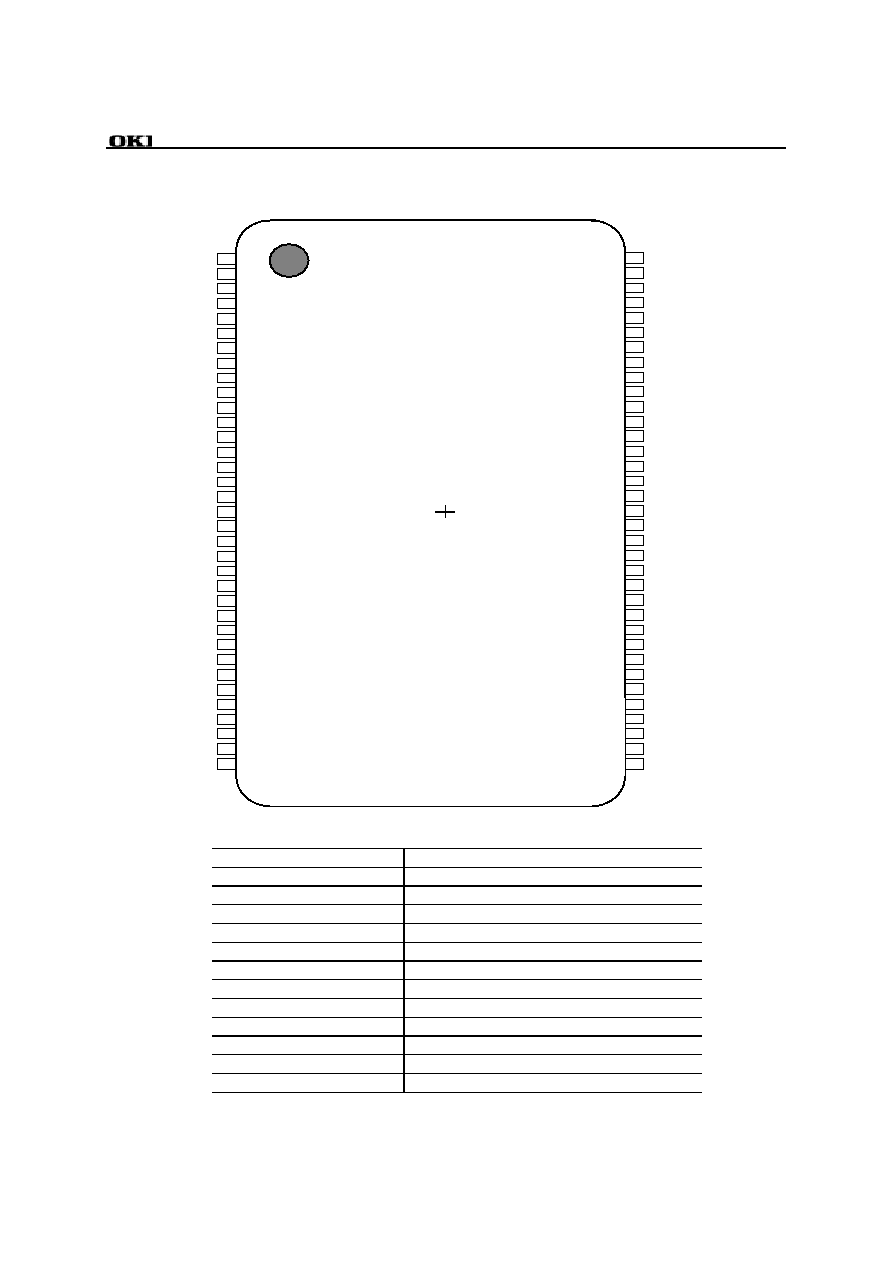
PIN CONFIGURATION (TOP VIEW)
70-pin Plastic TSOP
SWCK
Serial Write Clock
SRCK
Serial Read Clock
WE
Write Enable
RE
Read Enable
IE
Input Enable
OE
Output Enable
RSTW
Reset Write
RSTR
Reset Read
DI0-15
Data Input
DO0-15
Data Output
V
SS
Ground (0 V)
V
CC
Power Supply (3.3 V)
NC
No Connection
Note: The same power supply voltage must be provided to every V
CC
pin, and the same GND voltage
level must be provided to every V
SS
pin.
1
2
3
4
5
6
7
8
9
10
11
12
13
14
15
16
17
18
19
20
21
22
23
24
25
26
27
28
29
30
31
32
33
34
35
V
CC
NC
NC
NC
V
SS
DI0
DI1
DI2
DI3
V
SS
DO0
DO1
V
CC
DO2
DO3
V
SS
V
SS
V
CC
V
CC
DO4
DO5
V
CC
DO6
DO7
V
SS
DI4
DI5
DI6
DI7
V
SS
OE
RE
RSTR
SRCK
V
CC
70
69
68
67
66
65
64
63
62
61
60
59
58
57
56
55
54
53
52
51
50
49
48
47
46
45
44
43
42
41
40
39
38
37
36
V
SS
NC
NC
NC
V
CC
DI15
DI14
DI13
DI12
V
SS
DO15
DO14
V
CC
DO13
DO12
V
SS
V
SS
V
CC
V
CC
DO11
DO10
V
CC
DO9
DO8
V
SS
DI11
DI10
DI9
DI8
V
CC
IE
WE
RSTW
SWCK
V
SS

Semiconductor
MS81V06160
4/18
BLOCK DIAGRAM
Refresh
Counter
Data-output
Buffer
Read Data Register
X
Decoder
(X16)
Serial Read Controller
(X16)
Serial Write Controller
Data-input
Buffer
Read/Write
Refresh
Timing Generater
DO (X16)
OE
RE
RSTR
SRCK
DI (X16)
IE
WE
RSTW
SWCK
401,408 x 16
Memory
Array
Write Data Register

Semiconductor
MS81V06160
5/18
PIN DESCRIPTION
Data Inputs: (DI0-15)
These pins are used for serial data inputs.
Write Reset: RSTW
The first positive transition of SWCK after RSTW becomes high resets the write address pointers to zero. RSTW
setup and hold times are referenced to the rising edge of SWCK.
Write Enable: WE
WE is used for data write enable/disable control. WE high level enables the input, and WE low level disables the
input and holds the internal write address pointer. There are no WE disable time (low) and WE enable time (high)
restrictions, because the MS8106160 is in fully static operation as long as the power is on. Note that WE setup and
hold times are referenced to the rising edge of SWCK. The latency for the write operation control by WE is 2.
After write reset, WE must remain low for more than 1600 ns (tFWD). After write reset, the write operation at
address 0 is started after a time tWL form the cycle in which WE is brought high.
After write reset, WE should be remained high for 2 cycles after driving WE high first.
Input Enable: IE
IE is used to enable/disable writing into memory. IE high level enables writing. The internal write address pointer
is always incremented by cycling SWCK regardless of the IE level. Note that IE setup and hold times are
referenced to the rising edge of SWCK. The latency for the write operation control by IE is 2.
Data Out: (DO0-15)
These pins are used for serial data outputs.
Read Reset: RSTR
The first positive transition of SRCK after RSTR becomes high resets the read address pointers to zero.
RSTR setup and hold times are referenced to the rising edge of SRCK.
Read Enable: RE
The function of RE is to gate of the SRCK clock for incrementing the read pointer. When RE is high before the
rising edge of SRCK, the read pointer is incremented. When RE is low, the read pointer is not incremented. RE
setup times (tRENS and tRDSS) and RE hold times (tRENH and tRDSH) are referenced to the rising edge of the
SRCK clock.
The latency for the read operation control by RE is 2. After read reset, RE must remain low for more than 1600 ns
(tFRD). After read reset, the read data at address 0 is output after a time tRL from the cycle in which WE is brought
high.
After read reset, RE should be remained high for 2 cycles after driving RE high first.
Output Enable: OE
OE is used to enable/disable the outputs. OE high level enables the outputs. The internal read address pointer is
always incremented by cycling SRCK regardless of the OE level. Note that OE setup and hold times are referenced
to the rising edge of SRCK. The latency for the read operation control by OE is 2.

Semiconductor
MS81V06160
6/18
Serial Write Clock: SWCK
The SWCK latches the input data on chip when WE is high, and also increments the internal write address pointer.
Data-in setup time tDS, and hold time tDH are referenced to the rising edge of SWCK.
Serial Read Clock: SRCK
Data is shifted out of the data registers. It is triggered by the rising edge of SRCK when RE is high during a read
operation. The SRCK input increments the internal read address pointer when RE is high.
The three-state output buffer provides direct TTL compatibility (no pullup resistor required). Data out is the same
polarity as data in. The output becomes valid after the access time interval tAC that begins with the rising edge of
SRCK. *There are no output valid time restriction on MS8106160.
Semiconductor
MS81V06160
7/18
ELECTRICAL CHARACTERISTICS
Absolute Maximum Ratings
Parameter
Symbol
Condition
Rating
Unit
Power Supply Voltage
V
CC
Ta = 25∞C
∑
0.5 to +4.6
V
Input Output Voltage
V
T
Ta = 25∞C, V
SS
∑
0.5 to +4.6
V
Output Current
I
OS
Ta = 25∞C
50
mA
Power Dissipation
P
D
Ta = 25∞C
1
W
Operating Temperature
T
opr
--
0 to 70
∞C
Storage Temperature
T
stg
--
∑
55 to +150
∞C
Recommended Operating Conditions
Parameter
Symbol
Min.
Typ.
Max.
Unit
Power Supply voltage
V
CC
3.0
3.3
3.6
V
Input High Voltage
V
IH
2.0
V
CC
V
CC
+ 0.2
V
Input Low Voltage
V
IL
∑
0.3
0
0.8
V
DC Characteristics
Parameter
Symbol
Condition
Min.
Max.
Unit
Input Leakage Current
I
LI
0 < V
I
< V
CC
,
Other Pins Tested at V = 0 V
≠10
+10
µ
Output Leakage Current
I
LO
0 < V
O
< V
CC
≠10
+10
µ
Output "H" Level Voltage
V
OH
I
OH
= ≠2 mA
2.4
--
V
Output "L" Level Voltage
V
OL
I
OH
= 2 mA
--
0.4
V
≠12
--
210
Operating Current
I
CC1
Minimum Cycle Time
Output Open
≠15
--
170
mA
≠12
--
6
Standby Current
I
CC2
Input Pin = V
IH
/V
IL
≠15
--
6
mA
Capacitance
(V
CC
= 3.3 V ± 0.3 V, Ta = 25∞C, f = 1 MHz)
Parameter
Symbol
Max.
Unit
Input Capacitance
C
I
5
pF
Output Capacitance
C
O
7
pF

Semiconductor
MS81V06160
8/18
AC Characteristics
(V
CC
= 3.3 V ± 10%, Ta = 0 to 70∞C)
MS81V06160-12
MS81V06160-15
Parameter
Symbol
Min.
Max.
Min.
Max.
Unit
Access Time from SRCK
t
AC
--
9
--
12
ns
D
OUT
Hold Time from SRCK
t
DDCK
3
--
3
--
ns
D
OUT
Enable Time from SRCK
t
DECK
3
9
3
12
ns
SWCK "H" Pulse Width
t
WSWH
4
--
6
--
ns
SWCK "L" Pulse Width
t
WSWL
4
--
6
--
ns
Input Data Setup Time
t
DS
3
--
3
--
ns
Input Data Hold Time
t
DH
1
--
1.5
--
ns
WE Enable Setup Time
t
WENS
3
--
3
--
ns
WE Enable Hold Time
t
WENH
1
--
1.5
--
ns
WE Disable Setup Time
t
WDSS
3
--
3
--
ns
WE Disable Hold Time
t
WDSH
1
--
1.5
--
ns
IE Enable Setup Time
t
IENS
3
--
3
--
ns
IE Enable Hold Time
t
IENH
1
--
1.5
--
ns
IE Disable Setup Time
t
IDSS
3
--
3
--
ns
IE Disable Hold Time
t
IDSH
1
--
1.5
--
ns
WE "H" Pulse Width
t
WWEH
4
--
6
--
ns
WE "L" Pulse Width
t
WWEL
4
--
6
--
ns
IE "H" Pulse Width
t
WIEH
4
--
6
--
ns
IE "L" Pulse Width
t
WIEL
4
--
6
--
ns
RSTW Setup Time
t
RSTWS
3
--
3
--
ns
RSTW Hold Time
t
RSTWH
1
--
1.5
--
ns
SRCK "H" Pulse Width
t
WSRH
4
--
6
--
ns
SRCK "L" Pulse Width
t
WSRL
4
--
6
--
ns
RE Enable Setup Time
t
RENS
3
--
3
--
ns
RE Enable Hold Time
t
RENH
1
--
1.5
--
ns
RE Disable Setup Time
t
RDSS
3
--
3
--
ns
RE Disable Hold Time
t
RDSH
1
--
1.5
--
ns
OE Enable Setup Time
t
OENS
3
--
3
--
ns
OE Enable Hold Time
t
OENH
1
--
1.5
--
ns
OE Disable Setup Time
t
ODSS
3
--
3
--
ns
OE Disable Hold Time
t
ODSH
1
--
1.5
--
ns
RE "H" Pulse Width
t
WREH
4
--
6
--
ns
RE "L" Pulse Width
t
WREL
4
--
6
--
ns
OE "H" Pulse Width
t
WOEH
4
--
6
--
ns
OE "L" Pulse Width
t
WOEL
4
--
6
--
ns
RSTR Setup Time
t
RSTRS
3
--
3
--
ns
RSTR Hold Time
t
RSTRH
1
--
1.5
--
ns
SWCK Cycle Time
t
SWC
12
--
15
--
ns
SRCK Cycle Time
t
SRC
12
--
15
--
ns
Transition Time (Rise and Fall)
t
T
1
5
1
5
ns
WE "L" Period before W Reset
t
LWE
3
--
3
--
clk
RE "L" Period before R Reset
t
LRE
3
--
3
--
clk
RE Delay after Reset
t
FRD
1,600
--
1,600
--
ns
WE Delay after Reset
t
FWD
1,600
--
1,600
--
ns

Semiconductor
MS81V06160
9/18
Parameter
Symbol
MS81V06160-12, MS81V06160-15
Unit
Write Latency
t
WL
4
clk
Read Latency
t
RL
4
clk
WE Write Control Latency
t
WEL
2
clk
IE Write Control Latency
t
IEL
2
clk
RE Read Control Latency
t
REL
2
clk
OE Read Control Latency
t
OEL
2
clk
AC Characteristic Measuring Conditions
Output Compare Level
1.4 V
Output Load
1 TTL + 30 pF
Input Signal Level
3.0 V/0.0 V
Input Signal Rise/Fall Time
1 ns
Input Signal Measuring Reference Level
1.4 V
Note: Input voltage levels for the AC characteristic measurement are V
IH
= 3.0 V and V
IL
= 0 V.
When transition time t
T
becomes 1 ns or more, the input signal reference levels for the parameter
measurement are V
IH
(min.) and V
IL
(max.).

Semiconductor
MS81V06160
10/18
OPERATION MODE
Write Operation Cycle
The write operation is controlled by four control signals, SWCK, RSTW, WE, and IE. The write operation is
accomplished by cycling SWCK, and holding WE high after the write address pointer reset operation or RSTW.
RSTW must be performed for internal circuit initialization before write operation. WE must be low before and
after the reset cycle (t
LWE
+ t
FWD
).
Each write operation, which begins after RSTW must contain at least 231 active write cycles, i.e., SWCK cycles
while WE and IE are high.
Settings of WE and IE to the operation mode of Write address pointer and Data input.
WE
IE
Internal Write address pointer
Data input (Latency 2)
H
H
Input
H
L
Incremented
L
X
Halted
Not input
X indicates "don't care"
Read Operation Cycle
The read operation is controlled by four control signals, SRCK, RSTR, RE, and OE. The read operation is
accomplished by cycling SRCK, and holding both RE and OE high after the read address pointer reset operation or
RSTR.
Each read operation, which begins after RSTR, must contain at least 231 active read cycles, i.e., SRCK cycles
while RE and OE are high. RE must be low before and after the reset cycle (t
LRE
+ t
FWD
).
Settings of RE and OE to the operation mode of read address pointer and Data output.
RE
OE
Internal Read address pointer
Data output (Latency 2)
H
H
Output
H
L
Incremented
High impedance
L
H
Output
L
L
Halted
High impedance
Power-up and Initialization
On power-up, the device is designed to begin proper operation after at least 200
µ
s after Vcc has stabilized to a
value within the range of recommended operating conditions. After this 200
µ
s stabilization interval, the following
initialization sequence must be performed. Because the read and write address pointers are undefined after
power-up, a minimum of 330 dummy write operations (SWCK cycles) and read operations (SRCK cycles) must be
performed, followed by an RSTW operation and an RSTR operation, to properly initialize the write and the read
address pointer.

Semiconductor
MS81V06160
11/18
Old/New Data Access
There must be a minimum delay of 600 SWCK cycles between writing into memory and reading out from memory.
If reading from the first field starts with an RSTR operation, before the start of writing the second field (before the
next RSTW operation), then the data just written will be read out.
The start of reading out the first field of data may be delayed past the beginning of writing in the second field of
data for as many as 70 SWCK cycles. If the RSTR operation for the first field read-out occurs less than 70 SWCK
cycles after the RSTW operation for the second field write-in, then the internal buffering of the device assures that
the first field will still be read out. The first field of data that is read out while the second field of data is written is
called "old data". In order to read out "new data", i.e., the second field written in, read reset must be input after
write address 200 the delay between an RSTW operation and an RSTR operation must be at least 600 SRCK cycles.
If the delay between RSTW and RSTR operations is more than 71 but less than 600 cycles, then the data read out
will be undetermined. It may be "old data" or "new" data, or a combination of old and new data. Such a timing
should be avoided.
When the read address delay is between more than 71 and less than 599 or more than 401,408, read data will be
undetermined. However, normal write is achieved in this address codition.
Semiconductor
MS81V06160
12/18
TIMING DIAGRAM
Write Cycle Timing (Write Reset)
Write Cycle Timing (Write Enable)
SWCK
RSTW
DI 0-15
WE
IE
4 cycle
5 cycle
6 cycle
L
H
t
WDSS
t
WDSH
t
WENH
t
WENS
t
WWEL
t
WWEH
D4
D5
D6
D2
D1
D3
D0
1 cycle
2 cycle
3cycle
D7
t
WEL
SWCK
RSTW
DI 0-15
WE
IE
t
FWD
t
LWE
t
SWC
t
WSWH
D0
Dn-1
t
DS
t
DH
D1
Dn
0 cycle
t
WL
*After write reset, WE should be remained high for 2 cycles after driving WE high first.
t
RSTWH
t
RSTWS
t
WSWL

Semiconductor
MS81V06160
13/18
Write Cycle Timing (Input Enable)
SWCK
RSTW
DI 0-15
WE
IE
8 cycle
9 cycle 10 cycle
L
H
t
IDSS
t
IDSH
t
IENH
t
IENS
t
WIEL
t
WIEH
D8
D9
D10
D2
D1
D3
D0
1 cycle
2 cycle
3 cycle
D11
4 cycle
5 cycle
6 cycle
7 cycle
t
IEL

Semiconductor
MS81V06160
14/18
Read Cycle Timing (Read Reset)
Read Cycle Timing (Read Enable)
SRCK
RSTR
DO 0-15
RE
OE
4 cycle
t
AC
Q2
Q1
Q0
5 cycle
Q4
Q5
Q6
Q7
L
H
t
RDSS
t
RDSH
t
RENH
t
RENS
1 cycle
t
WREL
t
WREH
Q3
2 cycle
3 cycle
t
REL
DO 0-15
SRCK
RSTR
RE
OE
1 cycle
t
AC
Qn-1
Q0
Q1
t
RL
t
FRD
t
RSTRH
t
RSTRS
t
SRC
t
WSRH
t
LRE
0 cycle
H
Qn
*After write reset, RE should be remained high for 2 cycles after driving RE high first.
t
WSRL

Semiconductor
MS81V06160
15/18
Read Cycle Timing (Output Enable)
SRCK
RSTR
DO 0-15
RE
OE
8 cycle
t
AC
Q3
Q2
Q1
Q0
9 cycle
10 cycle 11 cycle
Q8
Q9
Q10
Q11
L
H
t
ODSS
t
ODSH
t
OENH
t
OENS
1 cycle
4 cycle
5 cycle
6 cycle
7 cycle
t
DECK
t
WOEL
t
WOEH
2 cycle
3 cycle
t
OEL
t
DDCK

Se
m
i
c
o
nd
uc
to
r
M
S
8
1
V061
60
16/
18
Read/Write Cycle Timing (New Data Read)

Se
m
i
c
o
nd
uc
to
r
M
S
8
1
V061
60
17/
18
Read/Write Cycle Timing (Old Data Read)
Semiconductor
MS81V06160
18/18
Read/Write Cycle T
i
m
i
ng