 | –≠–ª–µ–∫—Ç—Ä–æ–Ω–Ω—ã–π –∫–æ–º–ø–æ–Ω–µ–Ω—Ç: MSC23136D | –°–∫–∞—á–∞—Ç—å:  PDF PDF  ZIP ZIP |
Semiconductor
MSC23136D/DL-xxBS10/DS10
1,048,576-word x 36-bit DYNAMIC RAM MODULE : FAST PAGE MODE TYPE
This version: Feb. 23. 1999
DESCRIPTION
The MSC23136D/DL-xxBS10/DS10 is a fully decoded, 1,048,576-word x 36-bit CMOS dynamic random access
memory module composed of eight 4Mb DRAMs in SOJ packages and two 2Mb DRAMs in SOJ packages mounted
with ten decoupling capacitors on a 72-pin glass epoxy single-inline package. This module supports any application
where high density and large capacity of storage memory are required. The MSC23136DL (the low-power version) is
specially designed for lower-power applications.
FEATURES
∑ 1,048,576-word x 36-bit organization
∑ 72-pin socket insertable module
MSC23136D/DL-xxBS10 : Gold tab
MSC23136D/DL-xxDS10 : Solder tab
∑ Single +5V supply ± 10% tolerance
∑ Input
: TTL compatible
∑ Output
: TTL compatible, 3-state
∑ Refresh
: 1024cycles/16ms (1024cycles/128ms: L-version)
∑ /CAS before /RAS refresh, hidden refresh, /RAS only refresh capability
∑ Fast page mode capability
∑ Multi-bit test mode capability
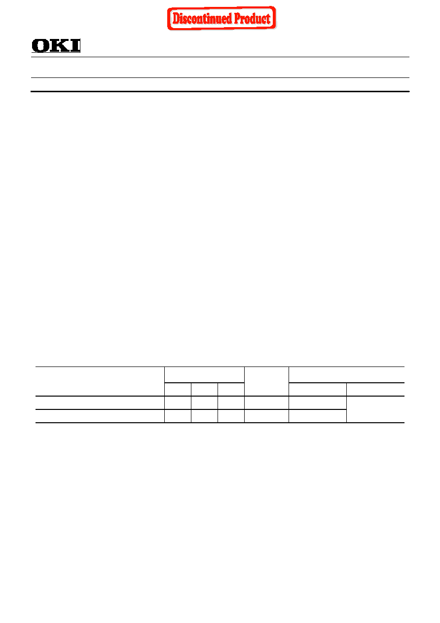
PRODUCT FAMILY
Access Time (Max.)
Power Dissipation
Family
t
RAC
t
AA
t
CAC
Cycle
Time
(Min.)
Operating(Max.)
Standby(Max.)
MSC23136D/DL-60BS10/DS10
60ns
30ns
15ns
110ns
4840mW
MSC23136D/DL-70BS10/DS10
70ns
35ns
20ns
130ns
4290mW
55mW/
9.9mW(L-version)

Semiconductor
MSC23136D/DL
MODULE OUTLINE
1
72
R1.57
6.35
1.04Typ.
1.27±0.1
95.25
2.03Typ.
6.35Typ.
Typ.
6.35
Typ.
10.16
3.18
25.4±0.2
101.19Typ.
107.95±0.2
*1
3.38Typ.
3.7Min.
5.28Max.
+0.1
-0.08
1.27
(Unit : mm)
MSC23136D/DL-xxBS10/DS10
*1
The common size difference of the board width 12.5mm of its height is specified as ±0.2.
The value above 12.5mm is specified as ±0.5.
Semiconductor
MSC23136D/DL
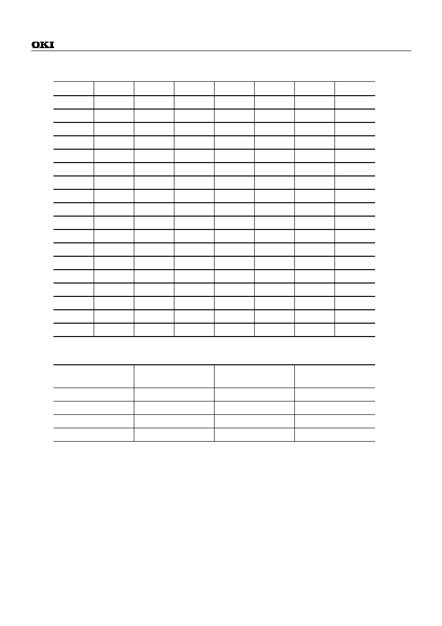
PIN CONFIGURATION
Pin No.
Pin Name
Pin No.
Pin Name
Pin No.
Pin Name
Pin No.
Pin Name
1
V
SS
19
NC
37
DQ17
55
DQ12
2
DQ0
20
DQ4
38
DQ35
56
DQ30
3
DQ18
21
DQ22
39
V
SS
57
DQ13
4
DQ1
22
DQ5
40
/CAS0
58
DQ31
5
DQ19
23
DQ23
41
/CAS2
59
V
CC
6
DQ2
24
DQ6
42
/CAS3
60
DQ32
7
DQ20
25
DQ24
43
/CAS1
61
DQ14
8
DQ3
26
DQ7
44
/RAS0
62
DQ33
9
DQ21
27
DQ25
45
NC
63
DQ15
10
V
CC
28
A7
46
NC
64
DQ34
11
NC
29
NC
47
/WE
65
DQ16
12
A0
30
V
CC
48
NC
66
NC
13
A1
31
A8
49
DQ9
67
PD1
14
A2
32
A9
50
DQ27
68
PD2
15
A3
33
NC
51
DQ10
69
PD3
16
A4
34
/RAS2
52
DQ28
70
PD4
17
A5
35
DQ26
53
DQ11
71
NC
18
A6
36
DQ8
54
DQ29
72
V
SS
Presence Detect Pins
Pin No.
Pin Name
MSC23136D/DL
-60BS10/DS10
MSC23136D/DL
-70BS10/DS10
67
PD1
V
SS
V
SS
68
PD2
V
SS
V
SS
69
PD3
NC
V
SS
70
PD4
NC
NC

Semiconductor
MSC23136D/DL
BLOCK DIAGRAM
/WE
/CAS0
/RAS0
A0-A9
/CAS1
DQ0
A0-A9
DQ
DQ
DQ
DQ
/OE
V
CC
/RAS
/CAS
/WE
V
SS
DQ1
DQ2
DQ3
DQ8
A0-A9
DQ1
DQ2
/OE
V
CC
/RAS
/CAS1
/WE
V
SS
DQ17
/CAS2
V
CC
V
SS
C1-C10
A0-A9
DQ
DQ
DQ
DQ
/OE
V
CC
/RAS
/CAS
/WE
V
SS
DQ4
DQ5
DQ6
DQ7
A0-A9
DQ
DQ
DQ
DQ
/OE
V
CC
/RAS
/CAS
/WE
V
SS
DQ9
DQ10
DQ11
DQ12
A0-A9
DQ
DQ
DQ
DQ
/OE
/RAS
/CAS
/WE
DQ13
DQ14
DQ15
DQ16
DQ18
A0-A9
DQ
DQ
DQ
DQ
/OE
/RAS
/CAS
/WE
DQ19
DQ20
DQ21
V
CC
V
SS
V
CC
V
SS
DQ22
A0-A9
DQ
DQ
DQ
DQ
/OE
/RAS
/CAS
/WE
DQ23
DQ24
DQ25
V
CC
V
SS
DQ26
A0-A9
DQ1
DQ2
/OE
V
CC
/RAS
/CAS1
/WE
V
SS
DQ35
/CAS2
DQ27
A0-A9
DQ
DQ
DQ
DQ
/OE
/RAS
/CAS
/WE
DQ28
DQ29
DQ30
V
CC
V
SS
DQ31
A0-A9
DQ
DQ
DQ
DQ
/OE
/RAS
/CAS
/WE
DQ32
DQ33
DQ34
V
CC
V
SS
/CAS2
/RAS2
/CAS3

Semiconductor
MSC23136D/DL
ELECTRICAL CHARACTERISTICS
Absolute Maximum Ratings
( Ta = 25∞C )
Parameter
Symbol
Rating
Unit
Voltage on Any Pin Relative to V
SS
V
IN
, V
OUT
-1.0 to +7.0
V
Voltage on V
CC
Supply Relative to V
SS
V
CC
-1.0 to +7.0
V
Short Circuit Output Current
I
OS
50
mA
Power Dissipation
P
D
10
W
Operating Temperature
T
OPR
0 to +70
∞C
Storage Temperature
T
STG
-40 to +125
∞C
Recommended Operating Conditions
( Ta = 0∞C to +70∞C )
Parameter
Symbol
Min.
Typ.
Max.
Unit
V
CC
4.5
5.0
5.5
V
Power Supply Voltage
V
SS
0
0
0
V
Input High Voltage
V
IH
2.4
-
6.5
V
Input Low Voltage
V
IL
-1.0
-
0.8
V
Capacitance
( V
CC
= 5V ± 10%, Ta = 25∞C, f = 1 MHz )
Parameter
Symbol
Typ.
Max.
Unit
Input Capacitance (A0 - A9)
C
IN1
-
70
pF
Input Capacitance (/WE)
C
IN2
-
80
pF
Input Capacitance (/RAS0, /RAS2)
C
IN3
-
43
pF
Input Capacitance (/CAS0- /CAS3)
C
IN4
-
24
pF
I/O Capacitance (DQ0 - DQ35)
C
DQ
-
13
pF
Note:
Capacitance measured with Boonton Meter.

Semiconductor
MSC23136D/DL
DC Characteristics
(V
CC
= 5V ± 10%, Ta = 0∞C to +70∞C )
MSC23136D/DL
-60BS10/DS10
MSC23136D/DL
-70BS10/DS10
Parameter
Symbo
l
Condition
Min.
Max.
Min.
Max.
Unit
Note
Input Leakage Current
I
LI
0V
V
IN
6.5V:
All other pins not
under test = 0V
-100
100
-100
100
µA
Output Leakage Current
I
LO
Data out is disable
0V
V
OUT
5.5V
-10
10
-10
10
µA
Output High Voltage
V
OH
I
OH
= -5.0mA
2.4
V
CC
2.4
V
CC
V
Output Low Voltage
V
OL
I
OL
= 4.2mA
0
0.4
0
0.4
V
Average Power Supply Current
(Operating)
I
CC1
/RAS cycling,
/CAS cycling,
t
RC
= min.
-
880
-
780
mA
1, 2
TTL
-
20
-
20
mA
1
-
10
-
10
mA
1
Power supply current
(Standby)
I
CC2
/RAS = V
IH
/CAS = V
IH
MOS
-
1.8
-
1.8
mA
1, 5
Average Power Supply Current
(/RAS only refresh)
I
CC3
/RAS cycling,
/CAS = V
IH
,
t
RC
= min.
-
880
-
780
mA
1, 2
Average Power Supply Current
(/CAS before /RAS refresh)
I
CC6
t
RC
= min.
-
880
-
780
mA
1, 2
Average Power Supply Current
(Fast Page Mode)
I
CC7
/RAS = V
IL
,
/CAS cycling,
t
PC
= min.
-
680
-
590
mA
1, 3
Average Power Supply Current
(Battery Backup)
I
CC10
t
RC
= 125µs,
/CAS before /RAS
cycling
-
2.8
-
2.8
mA
1, 4, 5
Notes: 1. I
CC
is dependent on output loading and cycles rates. Specified values are obtained with the output open.
2. Address can be changed once or less while /RAS = V
IL
.
3. Address can be changed once or less while /CAS = V
IH
.
4. V
CC
- 0.2V
V
IH
6.5V, - 1.0V
V
IL
0.2V.
5. L-version.

Semiconductor
MSC23136D/DL
AC Characteristics (1/2)
(V
CC
= 5V ± 10%, Ta = 0∞C to +70∞C ) Note: 1, 2, 3, 9, 10
MSC23136D/DL
-60BS10/DS10
MSC23136D/DL
-70BS10/DS10
Parameter
Symbol
Min.
Max.
Min.
Max.
Unit
Note
Random Read or Write Cycle Time
t
RC
110
-
130
-
ns
Fast Page Mode Cycle Time
t
PC
40
-
45
-
ns
Access Time from /RAS
t
RAC
-
60
-
70
ns
4, 5, 6
Access Time from /CAS
t
CAC
-
15
-
20
ns
4, 5
Access Time from Column Address
t
AA
-
30
-
35
ns
4, 6
Access Time from /CAS Precharge
t
CPA
-
35
-
40
ns
4
Output Low Impedance Time from /CAS
t
CLZ
0
-
0
-
ns
4
/CAS to Data Output Buffer Turn-off Delay Time
t
OFF
0
15
0
20
ns
7
Transition Time
t
T
3
50
3
50
ns
3
Refresh Period
t
REF
-
16
-
16
ms
Refresh Period (L-version)
t
REF
-
128
-
128
ms
/RAS Precharge Time
t
RP
40
-
50
-
ns
/RAS Pulse Width
t
RAS
60
10K
70
10K
ns
/RAS Pulse Width (Fast Page Mode)
t
RASP
60
100K
70
100K
ns
/RAS Hold Time
t
RSH
15
-
20
-
ns
/CAS Precharge Time (Fast Page Mode)
t
CP
10
-
10
-
ns
/CAS Pulse Width
t
CAS
15
10K
20
10K
ns
/CAS Hold Time
t
CSH
60
-
70
-
ns
/CAS to /RAS Precharge Time
t
CRP
5
-
5
-
ns
/RAS Hold Time from /CAS Precharge
t
RHCP
35
-
40
-
ns
/RAS to /CAS Delay Time
t
RCD
20
45
20
50
ns
5
/RAS to Column Address Delay Time
t
RAD
15
30
15
35
ns
6
Row Address Set-up Time
t
ASR
0
-
0
-
ns
Row Address Hold Time
t
RAH
10
-
10
-
ns
Column Address Set-up Time
t
ASC
0
-
0
-
ns
Column Address Hold Time
t
CAH
15
-
15
-
ns
Column Address Hold Time from /RAS
t
AR
50
-
55
-
ns
Column Address to /RAS Lead Time
t
RAL
30
-
35
-
ns
Read Command Set-up Time
t
RCS
0
-
0
-
ns
Read Command Hold Time
t
RCH
0
-
0
-
ns
8
Read Command Hold Time referenced to /RAS
t
RRH
0
-
0
-
ns
8

Semiconductor
MSC23136D/DL
AC Characteristics (2/2)
(V
CC
= 5V ± 10%, Ta = 0∞C to +70∞C ) Note: 1, 2, 3, 9, 10
MSC23136D/DL
-60BS10/DS10
MSC23136D/DL
-70BS10/DS10
Parameter
Symbol
Min.
Max.
Min.
Max.
Unit
Note
Write Command Set-up Time
t
W CS
0
-
0
-
ns
Write Command Hold Time
t
W CH
10
-
10
-
ns
Write Command Hold Time from /RAS
t
W CR
45
-
50
-
ns
Write Command Pulse Width
t
W P
10
-
10
-
ns
Write Command to /RAS Lead Time
t
RW L
15
-
20
-
ns
Write Command to /CAS Lead Time
t
CW L
15
-
20
-
ns
Data-in Set-up Time
t
DS
0
-
0
-
ns
Data-in Hold Time
t
DH
15
-
15
-
ns
Data-in Hold Time from /RAS
t
DHR
50
-
55
-
ns
/CAS Active Delay Time from /RAS Precharge
t
RPC
10
-
10
-
ns
/RAS to /CAS Set-up Time
(/CAS before /RAS)
t
CSR
5
-
5
-
ns
/RAS to /CAS Hold Time
(/CAS before /RAS)
t
CHR
10
-
10
-
ns
/WE to /RAS Precharge Time
(/CAS before /RAS)
t
W RP
10
-
10
-
ns
/WE Hold Time from /RAS
(/CAS before /RAS)
t
W RH
10
-
10
-
ns
/RAS to /WE Set-up Time
(Test Mode)
t
W TS
10
-
10
-
ns
/RAS to /WE Hold Time
(Test Mode)
t
W TH
10
-
10
-
ns

Semiconductor
MSC23136D/DL
Notes: 1. A start-up delay of 200µs is required after power-up, followed by a minimum of eight initialization cycles
(/RAS only refresh or /CAS before /RAS refresh) before proper device operation is achieved.
2. The AC characteristics assumes t
T
= 5ns.
3. V
IH
(Min.) and V
IL
(Max.) are reference levels for measuring input timing signals. Transition time (t
T
) are
measured between V
IH
and V
IL
.
4. This parameter is measured with a load circuit equivalent to 2TTL loads and 100pF.
5. Operation within the t
RCD
(Max.) limit ensures that t
RAC
(Max.) can be met.
t
RCD
(Max.) is specified as a reference point only. If t
RCD
is greater than the specified t
RCD
(Max.) limit, then
the access time is controlled by t
CAC
.
6. Operation within the t
RAD
(Max.) limit ensures that t
RAC
(Max.) can be met.
t
RAD
(Max.) is specified as a reference point only. If t
RAD
is greater than the specified t
RAD
(Max.) limit, then
the access time is controlled by t
AA
.
7. t
OFF
(Max.) define the time at which the output achieves the open circuit condition and are not referenced
to output voltage levels.
8. t
RCH
or t
RRH
must be satisfied for a read cycle.
9. The test mode is initiated by performing a /WE and /CAS before /RAS refresh cycle. This mode is
latched and remains in effect until the exit cycle is generated. The test mode specified in this data sheet
is a 2-bit parallel test function. CA0 is not used. In a read cycle, if all internal bits are equal, the DQ pin
will indicate a high level. If any internal bits are not equal, the DQ pin will indicate a low level.
The test mode is cleared and the memory device returned to its normal operating state by a /RAS only
refresh or /CAS before /RAS refresh cycle.
10. In a test mode read cycle, the value of access time parameters is delayed for 5ns for the specified value.
These parameters should be specified in test mode cycle by adding the above value to the specified
value in this data sheet.