
Semiconductor
MSC2323258D-xxBS4/DS4
2,097,152-word x 32-bit DYNAMIC RAM MODULE : FAST PAGE MODE TYPE WITH EDO
This version: Mar. 3. 1999
DESCRIPTION
The MSC2323258D-xxBS4/DS4 is a fully decoded, 2,097,152-word x 32-bit CMOS dynamic random access
memory module composed of four 16Mb DRAMs in SOJ packages mounted with eight decoupling capacitors on a
72-pin glass epoxy single-inline package. This module supports any application where high density and large
capacity of storage memory are required.
FEATURES
∑ 2,097,152-word x 32-bit organization
∑ 72-pin Single Inline Memory Module
MSC2323258D-xxBS4 : Gold tab
MSC2323258D-xxDS4 : Solder tab
∑ Single +5V supply ± 10% tolerance
∑ Input
: TTL compatible
∑ Output
: TTL compatible, 3-state
∑ Refresh
: 1024cycles/16ms
∑ /CAS before /RAS refresh, hidden refresh, /RAS only refresh capability
∑ Fast page mode with EDO capability
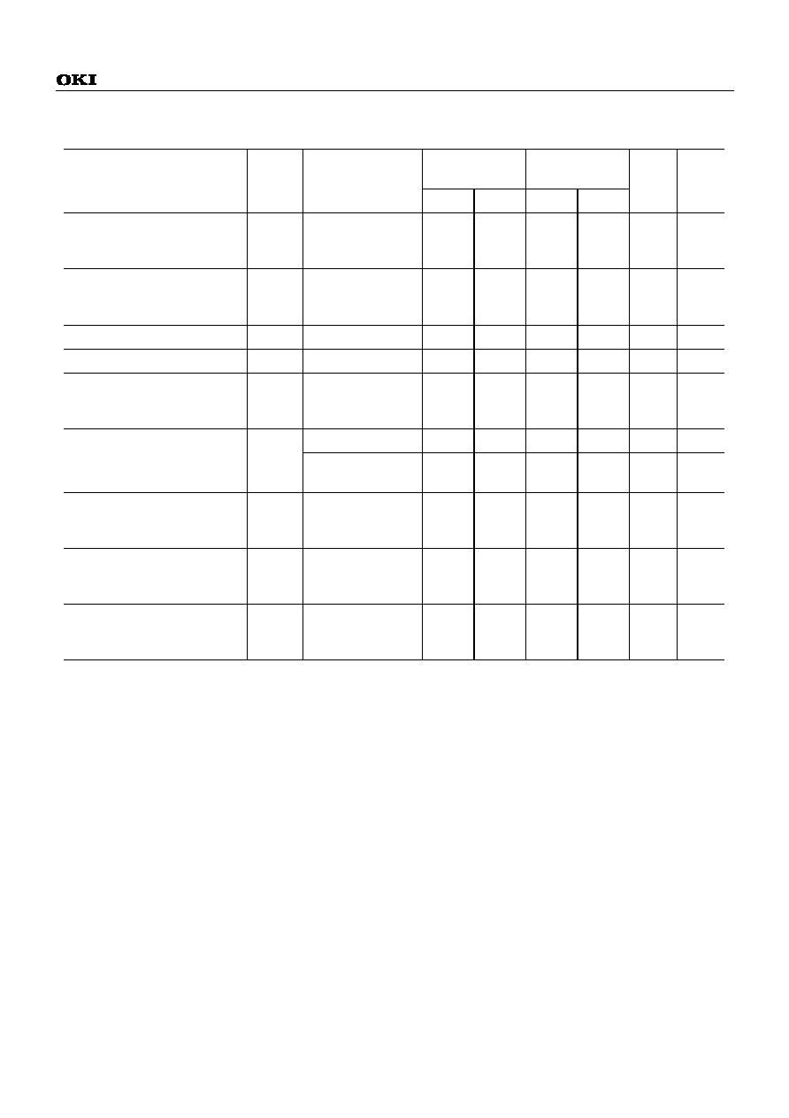
PRODUCT FAMILY
Access Time (Max.)
Power Dissipation
Family
t
RAC
t
AA
t
CAC
Cycle
Time
(Min.)
Operating (Max.)
Standby (Max.)
MSC2323258D-60BS4/DS4
60ns
30ns
15ns
104ns
1430mW
MSC2323258D-70BS4/DS4
70ns
35ns
20ns
124ns
1320mW
22mW

Semiconductor
MSC2323258D
MODULE OUTLINE
1
72
R1.57
6.35
1.04Typ.
1.27±0.1
95.25
2.03Typ.
6.35Typ.
Typ.
6.35
Typ.
10.16
3.18
19.0±0.2
101.19Typ.
107.95±0.2
*1
3.38Typ.
5.7Min.
9.3Max.
+0.1
-0.08
1.27
(Unit : mm)
MSC2323258D-xxBS4/DS4
*1
The common size difference of the board width 12.5mm of its height is specified as ±0.2.
The value above 12.5mm is specified as ±0.5.

Semiconductor
MSC2323258D
PIN CONFIGURATION
Pin No.
Pin Name
Pin No.
Pin Name
Pin No.
Pin Name
Pin No.
Pin Name
1
V
SS
19
NC
37
NC
55
DQ11
2
DQ0
20
DQ4
38
NC
56
DQ27
3
DQ16
21
DQ20
39
V
SS
57
DQ12
4
DQ1
22
DQ5
40
/CAS0
58
DQ28
5
DQ17
23
DQ21
41
/CAS2
59
V
CC
6
DQ2
24
DQ6
42
/CAS3
60
DQ29
7
DQ18
25
DQ22
43
/CAS1
61
DQ13
8
DQ3
26
DQ7
44
/RAS0
62
DQ30
9
DQ19
27
DQ23
45
/RAS1
63
DQ14
10
V
CC
28
A7
46
NC
64
DQ31
11
NC
29
NC
47
/WE
65
DQ15
12
A0
30
V
CC
48
NC
66
NC
13
A1
31
A8
49
DQ8
67
PD1
14
A2
32
A9
50
DQ24
68
PD2
15
A3
33
/RAS3
51
DQ9
69
PD3
16
A4
34
/RAS2
52
DQ25
70
PD4
17
A5
35
NC
53
DQ10
71
NC
18
A6
36
NC
54
DQ26
72
V
SS
Presence Detect Pins
Pin No.
Pin Name
MSC2323258D
-60BS4/DS4
MSC2323258D
-70BS4/DS4
67
PD1
NC
NC
68
PD2
NC
NC
69
PD3
NC
V
SS
70
PD4
NC
NC

Semiconductor
MSC2323258D
BLOCK DIAGRAM
/WE
/CAS1
/CAS0
A0-A9
/CAS3
/CAS2
DQ0
A0-A9
DQ1
DQ3
DQ2
DQ4
DQ5
/RAS
/LCAS
/UCAS
DQ6
DQ1
DQ2
DQ3
/RAS1
V
CC
V
SS
C1-C8
DQ8
V
SS
/WE
/OE
V
CC
DQ4
DQ5
DQ6
DQ7
DQ7
DQ8
DQ9
DQ11
DQ10
DQ12
DQ13
DQ14
DQ9
DQ10
DQ11
DQ16
DQ12
DQ13
DQ14
DQ15
DQ15
A0-A9
DQ1
DQ3
DQ2
DQ4
DQ5
/RAS
/LCAS
/UCAS
DQ6
DQ8
V
CC
/WE
/OE
V
SS
DQ7
DQ9
DQ11
DQ10
DQ12
DQ13
DQ14
DQ16
DQ15
/RAS0
/RAS2
/RAS3
DQ16
A0-A9
DQ1
DQ3
DQ2
DQ4
DQ5
/RAS
/LCAS
/UCAS
DQ6
DQ17
DQ18
DQ19
DQ8
V
SS
/WE
/OE
V
CC
DQ20
DQ21
DQ22
DQ23
DQ7
DQ24
DQ9
DQ11
DQ10
DQ12
DQ13
DQ14
DQ25
DQ26
DQ27
DQ16
DQ28
DQ29
DQ30
DQ31
DQ15
A0-A9
DQ1
DQ3
DQ2
DQ4
DQ5
/RAS
/LCAS
/UCAS
DQ6
DQ8
V
CC
/WE
/OE
V
SS
DQ7
DQ9
DQ11
DQ10
DQ12
DQ13
DQ14
DQ16
DQ15

Semiconductor
MSC2323258D
ELECTRICAL CHARACTERISTICS
Absolute Maximum Ratings
Parameter
Symbol
Rating
Unit
Voltage on Any Pin Relative to V
SS
V
IN
, V
OUT
-1.0 to +7.0
V
Voltage on V
CC
Supply Relative to V
SS
V
CC
-1.0 to +7.0
V
Short Circuit Output Current
I
OS
50
mA
Power Dissipation
P
D
*
4
W
Operating Temperature
T
OPR
0 to +70
∞C
Storage Temperature
T
STG
-40 to +125
∞C
* Ta = 25∞C
Recommended Operating Conditions
( Ta = 0∞C to +70∞C )
Parameter
Symbol
Min.
Typ.
Max.
Unit
V
CC
4.5
5.0
5.5
V
Power Supply Voltage
V
SS
0
0
0
V
Input High Voltage
V
IH
2.4
-
6.5
V
Input Low Voltage
V
IL
-1.0
-
0.8
V
Capacitance
( V
CC
= 5V ± 10%, Ta = 25∞C, f = 1 MHz )
Parameter
Symbol
Typ.
Max.
Unit
Input Capacitance (A0 - A9)
C
IN1
-
32
pF
Input Capacitance (/WE)
C
IN2
-
35
pF
Input Capacitance (/RAS0- /RAS3)
C
IN3
-
13
pF
Input Capacitance (/CAS0- /CAS3)
C
IN4
-
20
pF
I/O Capacitance (DQ0 - DQ31)
C
DQ
-
25
pF
Note:
Capacitance measured with Boonton Meter.
Semiconductor
MSC2323258D
DC Characteristics
(V
CC
= 5V ± 10%, Ta = 0∞C to +70∞C )
MSC2323258D
-60BS4/DS4
MSC2323258D
-70BS4/DS4
Parameter
Symbo
l
Condition
Min.
Max.
Min.
Max.
Unit
Note
Input Leakage Current
I
LI
0V
V
IN
6.5V;
All other pins not
under test = 0V
-40
40
-40
40
µA
Output Leakage Current
I
LO
DQ disable
0V
V
OUT
5.5V
-20
20
-20
20
µA
Output High Voltage
V
OH
I
OH
= -5.0mA
2.4
V
CC
2.4
V
CC
V
Output Low Voltage
V
OL
I
OL
= 4.2mA
0
0.4
0
0.4
V
Average Power Supply Current
(Operating)
I
CC1
/RAS, /CAS cycling,
t
RC
= Min.
-
260
-
240
mA
1, 2
/RAS, /CAS = V
IH
-
8
-
8
mA
1
Power supply current
(Standby)
I
CC2
/RAS, /CAS
V
CC
-0.2V
-
4
-
4
mA
1
Average Power Supply Current
(/RAS only refresh)
I
CC3
/RAS cycling,
/CAS = V
IH
,
t
RC
= Min.
-
260
-
240
mA
1, 2
Average Power Supply Current
(/CAS before /RAS refresh)
I
CC6
/RAS cycling,
/CAS before /RAS
-
260
-
240
mA
1, 2
Average Power Supply Current
(Fast Page Mode)
I
CC7
/RAS = V
IL
,
/CAS cycling,
t
HPC
= Min.
-
260
-
240
mA
1, 3
Notes: 1. I
CC
Max. is specified as I
CC
for output open condition.
2. Address can be changed once or less while /RAS = V
IL
.
3. Address can be changed once or less while /CAS = V
IH
.

Semiconductor
MSC2323258D
AC Characteristics (1/2)
(V
CC
= 5V ± 10%, Ta = 0∞C to +70∞C ) Note: 1, 2, 3
MSC2323258D
-60BS4/DS4
MSC2323258D
-70BS4/DS4
Parameter
Symbol
Min.
Max.
Min.
Max.
Unit
Note
Random Read or Write Cycle Time
t
RC
104
-
124
-
ns
Fast Page Mode Cycle Time
t
HPC
25
-
30
-
ns
Access Time from /RAS
t
RAC
-
60
-
70
ns
4, 5, 6
Access Time from /CAS
t
CAC
-
15
-
20
ns
4, 5
Access Time from Column Address
t
AA
-
30
-
35
ns
4, 6
Access Time from /CAS Precharge
t
CPA
-
35
-
40
ns
4
Output Low Impedance Time from /CAS
t
CLZ
0
-
0
-
ns
4
Data Output Hold After /CAS Low
t
DOH
5
-
5
-
ns
/CAS to Data Output Buffer Turn-off Delay Time
t
CEZ
0
15
0
20
ns
7, 8
/RAS to Data Output Buffer Turn-off Delay Time
t
REZ
0
15
0
20
ns
7, 8
/WE to Data Output Buffer Turn-off Delay Time
t
W EZ
0
15
0
20
ns
7
Transition Time
t
T
1
50
1
50
ns
3
Refresh Period
t
REF
-
16
-
16
ms
/RAS Precharge Time
t
RP
40
-
50
-
ns
/RAS Pulse Width
t
RAS
60
10K
70
10K
ns
/RAS Pulse Width (Fast Page Mode with EDO)
t
RASP
60
100K
70
100K
ns
/RAS Hold Time
t
RSH
10
-
13
-
ns
/CAS Precharge Time (Fast Page Mode with EDO)
t
CP
10
-
10
-
ns
/CAS Pulse Width
t
CAS
10
10K
13
10K
ns
/CAS Hold Time
t
CSH
40
-
45
-
ns
/CAS to /RAS Precharge Time
t
CRP
5
-
5
-
ns
/RAS Hold Time from /CAS Precharge
t
RHCP
35
-
40
-
ns
/RAS to /CAS Delay Time
t
RCD
14
45
14
50
ns
5
/RAS to Column Address Delay Time
t
RAD
12
30
12
35
ns
6
Row Address Set-up Time
t
ASR
0
-
0
-
ns
Row Address Hold Time
t
RAH
10
-
10
-
ns
Column Address Set-up Time
t
ASC
0
-
0
-
ns
Column Address Hold Time
t
CAH
10
-
13
-
ns
Column Address to /RAS Lead Time
t
RAL
30
-
35
-
ns
Read Command Set-up Time
t
RCS
0
-
0
-
ns
Read Command Hold Time
t
RCH
0
-
0
-
ns
9
Read Command Hold Time referenced to /RAS
t
RRH
0
-
0
-
ns
9

Semiconductor
MSC2323258D
AC Characteristics (2/2)
(V
CC
= 5V ± 10%, Ta = 0∞C to +70∞C ) Note: 1, 2, 3
MSC2323258D
-60BS4/DS4
MSC2323258D
-70BS4/DS4
Parameter
Symbol
Min.
Max.
Min.
Max.
Unit
Note
Write Command Set-up Time
t
W CS
0
-
0
-
ns
Write Command Hold Time
t
W CH
10
-
13
-
ns
Write Command Pulse Width
t
W P
10
-
10
-
ns
/WE Pulse Width (DQ Disable)
t
W PE
10
-
10
-
ns
Write Command to /RAS Lead Time
t
RW L
10
-
13
-
ns
Write Command to /CAS Lead Time
t
CW L
10
-
13
-
ns
Data-in Set-up Time
t
DS
0
-
0
-
ns
Data-in Hold Time
t
DH
10
-
13
-
ns
/CAS Active Delay Time from /RAS Precharge
t
RPC
5
-
5
-
ns
/RAS to /CAS Set-up Time
(/CAS before /RAS)
t
CSR
5
-
5
-
ns
/RAS to /CAS Hold Time
(/CAS before /RAS)
t
CHR
10
-
10
-
ns

Semiconductor
MSC2323258D
Notes: 1. A start-up delay of 200µs is required after power-up, followed by a minimum of eight initialization cycles
(/RAS only refresh or /CAS before /RAS refresh) before proper device operation is achieved.
2. The AC characteristics assumes t
T
= 2ns.
3. V
IH
(Min.) and V
IL
(Max.) are reference levels for measuring input timing signals. Transition time (t
T
) are
measured between V
IH
and V
IL
.
4. This parameter is measured with a load circuit equivalent to 2TTL loads and 100pF.
5. Operation within the t
RCD
(Max.) limit ensures that t
RAC
(Max.) can be met.
t
RCD
(Max.) is specified as a reference point only. If t
RCD
is greater than the specified t
RCD
(Max.) limit, then
the access time is controlled by t
CAC
.
6. Operation within the t
RAD
(Max.) limit ensures that t
RAC
(Max.) can be met.
t
RAD
(Max.) is specified as a reference point only. If t
RAD
is greater than the specified t
RAD
(Max.) limit, then
the access time is controlled by t
AA
.
7. t
CEZ
(Max.), t
REZ
(Max.) and t
W EZ
(Max.) define the time at which the output achieves the open circuit
condition and are not referenced to output voltage levels.
8. t
CEZ
and t
REZ
must be satisfied for open circuit condition.
9. t
RCH
or t
RRH
must be satisfied for a read cycle.