Semiconductor
MSM514265E/ESL
Preliminary
262,144-Word x 16-Bit DYNAMIC RAM : FAST PAGE MODE TYPE WITH EDO
DESCRIPTION
The MSM514265E/ESL is a 262,144-word
◊
16-bit dynamic RAM fabricated in Oki's silicon-gate CMOS
technology. The MSM514265E/ESL achieves high integration, high-speed operation, and low-power
consumption because Oki manufactures the device in a quadruple-layer polysilicon/double-layer metal CMOS
process. The MSM514265E/ESL is available in a 40-pin plastic SOJ or 44/40-pin plastic TSOP. The
MSM514265ESL (the Self-refresh version) is specially designed for lower-power applications.
FEATURES
∑
262,144-word
◊
16-bit configuration
∑
Single 5V power supply,
±
10
%
tolerance
∑
Input
: TTL compatible, low input capacitance
∑
Output
: TTL compatible, 3-state
∑
Refresh
: 512 cycles/8ms, 512 cycles/128 ms (SL version)
∑
Fast page mode with EDO, read modify write capability
∑
CAS before RAS refresh, hidden refresh, RAS-only refresh capability
∑
CAS before RAS self-refresh capability (SL version)
∑
Package options:
40-pin 400mil plastic SOJ
(SOJ40-P-400-1.27)
(Product : MSM514265E/ESL-xxJS)
44/40-pin 400mil plastic TSOP (TSOPII44/40-P-400-0.80-K) (Product : MSM514265E./ESL-xxTS-K)
xx indicates speed rank.
PRODUCT FAMILY
Access Time (Max.)
Power Dissipation
Family
t
RAC
t
AA
t
CAC
t
OEA
Cycle Time
(Min.)
Operating (Max.)
Standby (Max.)
60ns
30ns
15ns
15ns
104ns
633mW
MSM514265E/ESL
70ns
35ns
20ns
20ns
124ns
578mW
5.5mW/
1.1mW (SL version)
PEDD514265ESL-01
This version : Jan. 2001
MSM514265E/ESL
PEDD514265ESL-01
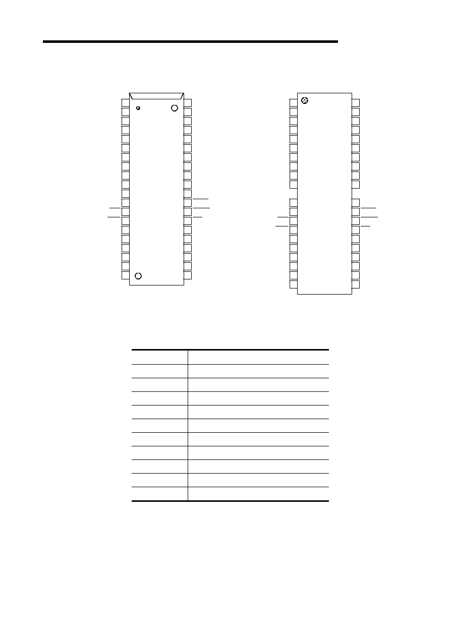
PIN CONFIGRATION (TOP VIEW)
Pin Name
Function
A0
-
A8
Address Input
RAS
Row Address Strobe
LCAS
Lower Byte Column Address Strobe
UCAS
Upper Byte Column Address Strobe
DQ1≠DQ16
Data Input/Data Output
OE
Output Enable
WE
Write Enable
V
CC
Power Supply (5V)
V
SS
Ground (0V)
NC
No Connection
Note : The same power supply voltage must be provided to every V
CC
pin, and the same
GND voltage level must be provided to every V
SS
pin.
40-Pin Plastic SOJ
44/40-Pin Plastic TSOP
(K Type)
1
2
3
4
5
6
7
8
9
10
11
12
13
14
15
16
17
18
19
20
21
40
39
38
37
36
35
34
33
32
31
30
29
28
27
26
25
24
23
22
DQ1
DQ2
DQ3
DQ4
V
CC
V
CC
V
CC
V
SS
V
SS
V
SS
DQ16
DQ15
DQ14
DQ13
DQ12
DQ11
DQ10
DQ9
A8
A7
A6
A0
A1
A2
A3
DQ5
DQ6
DQ7
DQ8
NC
NC
WE
RAS
NC
NC
A5
A4
LCAS
UCAS
OE
44
43
42
41
40
36
35
39
38
32
31
30
V
SS
V
SS
V
SS
DQ16
DQ15
DQ14
DQ13
DQ12
DQ11
DQ10
DQ9
A8
A7
A6
A5
A4
LCAS
UCAS
OE
29
28
27
26
NC
1
2
3
4
5
6
7
8
9
10
DQ1
DQ2
DQ3
DQ4
V
CC
V
CC
DQ5
DQ6
DQ7
DQ8
16
17
18
19
20
21
22
23
24
25
V
CC
A0
A1
A2
A3
NC
WE
RAS
NC
15
NC
14
13
37
MSM514265E/ESL
PEDD514265ESL-01
BLOCK DIAGRAM
FUNCTION TABLE
Input Pin
DQ Pin
RAS
RAS
RAS
RAS
LCAS
LCAS
LCAS
LCAS
UCAS
UCAS
UCAS
UCAS
WE
WE
WE
WE
OE
OE
OE
OE
DQ1-DQ8
DQ9-DQ16
Function Mode
H
*
*
*
*
High-Z
High-Z
Standby
L
H
H
*
*
High-Z
High-Z
Refresh
L
L
H
H
L
D
OUT
High-Z
Lower Byte Read
L
H
L
H
L
High-Z
D
OUT
Upper Byte Read
L
L
L
H
L
D
OUT
D
OUT
Word Read
L
L
H
L
H
D
IN
Don't Care
Lower Byte Write
L
H
L
L
H
Don't Care
D
IN
Upper Byte Write
L
L
L
L
H
D
IN
D
IN
Word Write
L
L
L
H
H
High-Z
High-Z
* : "H" or "L"
A0
A8
8
8
8
8
8
8
8
16
8
16
9
9
9
9
Timing
Generator
Column
Address
Buffers
I/O
Controller
Internal
Address
Counter
Row
Address
Buffers
Refresh
Control Clock
I/O
Controller
Column Decoders
Sense Amplifiers
Memory
Cells
Word
Drivers
Row
Deco-
ders
I/O
Selector
Input
Buffers
Input
Buffers
Output
Buffers
Output
Buffers
DQ1
DQ8
DQ9
DQ16
OE
WE
RAS
LCAS
UCAS
V
CC
V
SS
On Chip
V
BB
Generator
MSM514265E/ESL
PEDD514265ESL-01
ELECTRICAL CHARACTERISTICS
Absolute Maximum Ratings
Parameter
Symbol
Rating
Unit
Voltage
on
Any Pin Relative to V
SS
V
IN
, V
OUT
-
0.5 to V
CC
+
0.5
V
Voltage V
CC
supply Relative to V
SS
V
CC
-
0.5 to 7.0
V
Short Circuit Output Current
I
OS
50
mA
Power Dissipation
P
D*
1
W
Operating Temperature
T
opr
0 to 70
∞C
Storage Temperature
T
stg
-
55 to 150
∞C
*: Ta = 25
∞
C
Recommended Operating Conditions
(Ta = 0∞C to 70∞C)
Parameter
Symbol
Min.
Typ.
Max.
Unit
V
CC
4.5
5.0
5.5
V
Power Supply Voltage
V
SS
0
0
0
V
Input High Voltage
V
IH
2.4
V
CC
+
0.5
*1
V
Input Low Voltage
V
IL
-
0.5
*2
0.8
V
Notes:
*1. The input voltage is V
CC
+
2.0V when the pulse width is less than 20ns (the pulse width is with
respect to the point at which V
CC
is applied).
*2. The input voltage is V
SS
-
2.0V when the pulse width is less than 20ns (the pulse width respect to
the point at which V
SS
is applied).
Capacitance
(V
CC
= 5V
±
10
%
, Ta = 25∞C, f=1MHz)
Parameter
Symbol
Typ.
Max.
Unit
Input Capacitance (A0 ≠ A8)
C
IN1
5
pF
Input Capacitance
(
RAS
,
LCAS
,
UCAS
,
WE
,
OE
)
C
IN2
7
pF
Output Capacitance (DQ1 - DQ16)
C
I/O
7
pF
MSM514265E/ESL
PEDD514265ESL-01
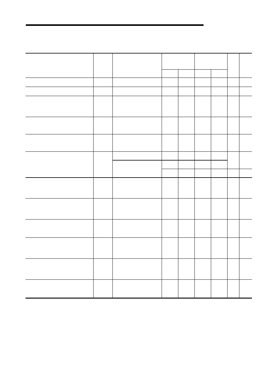
DC Characteristics
(V
CC
= 5V
±
10
%
, Ta = 0∞C to 70∞C)
MSM514265
E/ESL-60
MSM514265
E/ESL-70
Parameter
Symbol
Condition
Min.
Max.
Min.
Max.
Unit Note
Output High Voltage
V
OH
I
OH
=
-
5.0mA
2.4
V
CC
2.4
V
CC
V
Output Low Voltage
V
OL
I
OL
= 4.2mA
0
0.4
0
0.4
V
Input Leakage Current
I
LI
0V
V
I
V
CC
+
0.5V;
All other pins not
under test = 0V
-
10
10
-
10
10
µ
A
Output Leakage Current
I
LO
DQ disable
0V
V
O
V
CC
-
10
10
-
10
10
µ
A
Average Power Supply Current
(Operating)
I
CC1
RAS
,
CAS
cycling,
t
RC
= Min.
115
105
mA
1,2
RAS
,
CAS
= V
IH
2
2
1
1
mA
1
Power Supply Current
(Standby)
I
CC2
RAS
,
CAS
V
CC
-
0.2V
200
200
µ
A
1,5
Average Power Supply Current
(
RAS
-only Refresh)
I
CC3
RAS
cycling,
CAS
= V
IH
,
t
RC
= Min.
115
105
mA
1,2
Power Supply Current
(Standby)
I
CC5
RAS
= V
IH
,
CAS
= V
IL
,
DQ = enable
5
5
mA
1
Average Power Supply Current
(
CAS
before
RAS
Refresh)
I
CC6
RAS
= cycling,
CAS
before
RAS
115
105
mA
1,2
Average Power Supply Current
(Fast Page Mode)
I
CC7
RAS
= V
IL
,
CAS
cycling,
t
HPC
= Min.
115
105
mA
1,3
Average Power Supply Current
(Battery Backup)
I
CC10
t
RC
= 125
µ
s
CAS
before
RAS
t
RAS
= 1
µ
s
300
300
µ
A
1,4
,5
Average Power Supply Current
(
CAS
before
RAS
Self-Refresh)
I
CCS
RAS
0.2V,
CAS
0.2V,
300
300
µ
A
1,5
Notes: 1.
I
CC
Max. is specified as I
CC
for output open condition.
2.
The address can be changed once or less while
RAS = V
IL
.
3.
The address can be changed once or less while
CAS = V
IH
.
4.
V
CC
-
0.2V
V
IH
V
CC
+
0.5V,
-
0.5V
V
IL
0.2V.
5.
SL version.