1/15
° Semiconductor
MSM518128/L
DESCRIPTION
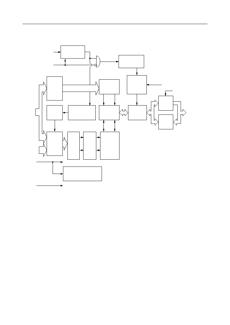
The MSM518128/L is a 131,072-word • 8-bit dynamic RAM fabricated in Oki's silicon-gate CMOS
technology. The MSM518128/L achieves high integration, high-speed operation, and low-power
consumption because Oki manufactures the device in a quadruple-layer polysilicon/single-layer
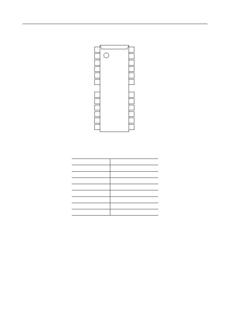
metal CMOS process. The MSM518128/L is available in a 26/24-pin plastic SOJ. The MSM518128L
(the low-power version) is specially designed for lower-power applications.
FEATURES
∑ 131,072-word • 8-bit configuration
∑ Single 5 V power supply,
±
5% tolerance
∑ Input
: TTL compatible, low input capacitance
∑ Output : TTL compatible, 3-state
∑ Refresh : 512 cycles/8 ms, 512 cycles/64 ms (L-version)
∑ Fast page mode, read modify write capability
∑ CAS before RAS refresh, hidden refresh, RAS-only refresh capability
∑ Package:
26/24-pin 300 mil plastic SOJ
(SOJ26/24-P-300-1.27) (Product : MSM518128/L-xxJS)
xx indicates speed rank.
PRODUCT FAMILY
° Semiconductor
MSM518128/L
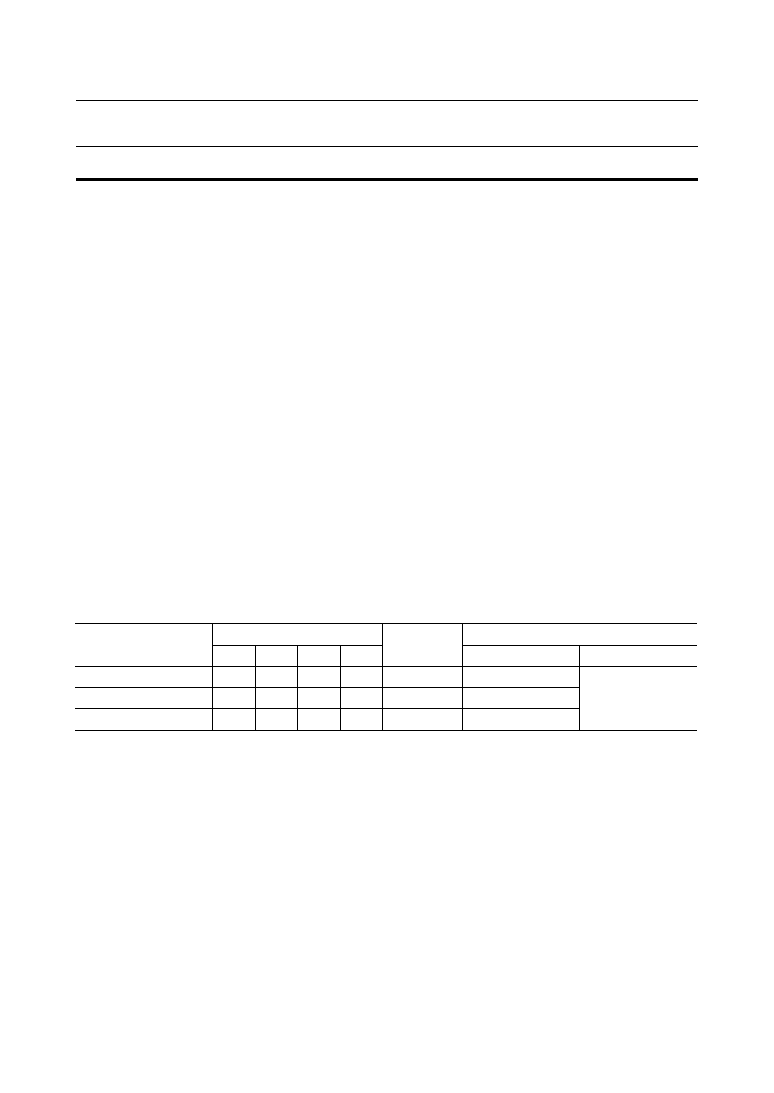
131,072-Word
• 8-Bit DYNAMIC RAM : FAST PAGE MODE TYPE
MSM518128/L-50
50 ns
100 ns
120 ns
630 mW
525 mW
5.25 mW/
Family
Access Time (Max.)
Cycle Time
(Min.)
Standby (Max.)
Power Dissipation
MSM518128/L-60
t
RAC
60 ns
26 ns
t
AA
30 ns
14 ns
t
CAC
15 ns
14 ns
t
OEA
15 ns
MSM518128/L-45
45 ns
90 ns
682.5 mW
24 ns
13 ns
13 ns
Operating (Max.)
1.05 mW (L-version)
E2G0012-17-41
This version: Jan. 1998
Previous version: May 1997
4/15
° Semiconductor
MSM518128/L
ELECTRICAL CHARACTERISTICS
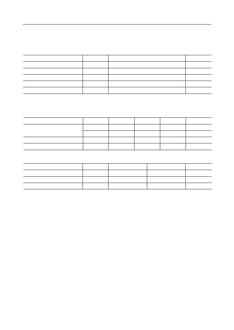
Absolute Maximum Ratings
Recommended Operating Conditions
Capacitance
*: Ta = 25
∞
C
Voltage on Any Pin Relative to V
SS
Short Circuit Output Current
Power Dissipation
Operating Temperature
Storage Temperature
V
T
Symbol
I
OS
P
D
*
T
opr
T
stg
≠1.0 to 7.0
50
1
0 to 70
≠55 to 150
Rating
mA
W
∞C
∞C
Parameter
V
Unit
Power Supply Voltage
Input High Voltage
Input Low Voltage
V
CC
Symbol
V
SS
V
IH
V
IL
5.0
0
--
--
Typ.
Parameter
4.75
0
2.4
≠1.0
Min.
5.25
0
6.5
0.8
Max.
(Ta = 0∞C to 70∞C)
V
Unit
V
V
V
Input Capacitance (A0 - A7, A8R)
Input Capacitance (RAS, CAS, WE, OE)
Output Capacitance (DQ1 - DQ8)
C
IN1
Symbol
C
IN2
C
I/O
6
7
7
Max.
pF
Unit
pF
pF
Parameter
(V
CC
= 5 V ±5%, Ta = 25∞C, f = 1 MHz)
--
--
--
Typ.
5/15
° Semiconductor
MSM518128/L
DC Characteristics
Parameter
Symbol
Condition
MSM518128
/L-45
MSM518128
/L-50
MSM518128
/L-60
(V
CC
= 5 V ±5%, Ta = 0∞C to 70∞C)
I
OH
= ≠5.0 mA
Output High Voltage
I
OL
= 4.2 mA
Output Low Voltage
0 V £ V
I
£ 6.5 V;
All other pins not
Input Leakage Current
under test = 0 V
DQ disable
Output Leakage Current
0 V £ V
O
£ 5.25 V
RAS, CAS cycling,
Average Power
t
RC
= Min.
Supply Current
(Operating)
RAS, CAS = V
IH
Power Supply
RAS, CAS
Current (Standby)
RAS cycling,
Average Power
CAS = V
IH
,
Supply Current
t
RC
= Min.
(RAS-only Refresh)
RAS = V
IH
,
Power Supply
CAS = V
IL
,
Current (Standby)
DQ = enable
Average Power
CAS before RAS
Supply Current
(CAS before RAS Refresh)
RAS = V
IL
,
Average Power
CAS cycling,
Supply Current
t
PC
= Min.
(Fast Page Mode)
t
RC
= 125 ms,
Average Power
V
OH
V
OL
I
LI
I
LO
I
CC1
I
CC2
I
CC3
I
CC5
I
CC6
I
CC7
I
CC10
CAS before RAS,
Supply Current
t
RAS
£ 1 ms
(Battery Backup)
V
CC
≠0.2 V
Min.
2.4
0
≠10
≠10
--
--
--
--
--
--
--
--
--
Max.
V
CC
0.4
10
10
130
2
1
130
5
130
100
300
200
Min.
2.4
0
≠10
≠10
--
--
--
--
--
--
--
--
--
Max.
V
CC
0.4
10
10
120
2
1
120
5
120
90
300
200
Min.
2.4
0
≠10
≠10
--
--
--
--
--
--
--
--
--
Max.
V
CC
0.4
10
10
100
2
1
100
5
100
80
300
200
Unit
V
V
mA
mA
mA
mA
mA
mA
mA
mA
mA
mA
Note
1, 2
1
1, 2
1
1, 2
1, 3
1, 4,
5
1, 5
RAS cycling,
Notes : 1. I
CC
Max. is specified as I
CC
for output open condition.
2. The address can be changed once or less while RAS = V
IL
.
3. The address can be changed once or less while CAS = V
IH
.
4. V
CC
≠ 0.2 V £ V
IH
£ 6.5 V, ≠1.0 V £ V
IL
£ 0.2 V.
5. L-version.