° Semiconductor
MSM51V17805D/DSL
1/17
DESCRIPTION
The MSM51V17805D/DSL is a 2,097,152-word • 8-bit dynamic RAM fabricated in Oki's silicon-gate
CMOS technology. The MSM51V17805D/DSL achieves high integration, high-speed operation,
and low-power consumption because Oki manufactures the device in a quadruple-layer polysilicon/
double-layer metal CMOS process. The MSM51V17805D/DSL is available in a 28-pin plastic SOJ or
28-pin plastic TSOP. The MSM51V17805DSL (the self-refresh version) is specially designed for
lower-power applications.
FEATURES
∑ 2,097,152-word • 8-bit configuration
∑ Single 3.3 V power supply,
±
0.3 V tolerance
∑ Input
: LVTTL compatible, low input capacitance
∑ Output : LVTTL compatible, 3-state
∑ Refresh : 2048 cycles/32 ms, 2048 cycles/128 ms (SL version)
∑ Fast page mode with EDO, read modify write capability
∑ CAS before RAS refresh, hidden refresh, RAS-only refresh capability
∑ CAS before RAS self-refresh capability (SL version)
∑ Multi-bit test mode capability
∑ Package options:
28-pin 400 mil plastic SOJ
(SOJ28-P-400-1.27)
(Product : MSM51V17805D/DSL-xxJS)
28-pin 400 mil plastic TSOP
(TSOPII28-P-400-1.27-K) (Product : MSM51V17805D/DSL-xxTS-K)
xx indicates speed rank.
PRODUCT FAMILY
° Semiconductor
MSM51V17805D/DSL
2,097,152-Word
• 8-Bit DYNAMIC RAM : FAST PAGE MODE TYPE WITH EDO
MSM51V17805D/DSL-70 70 ns
124 ns
84 ns
288 mW
360 mW
Family
Access Time (Max.)
Cycle Time
(Min.)
Standby (Max.)
Power Dissipation
MSM51V17805D/DSL-50
t
RAC
50 ns
35 ns
t
AA
25 ns
20 ns
t
CAC
13 ns
20 ns
t
OEA
13 ns
MSM51V17805D/DSL-60 60 ns
104 ns
324 mW
30 ns
15 ns
15 ns
Operating (Max.)
1.8 mW/
0.72 mW (SL version)
Preliminary
E2G0129-17-61
This version: Mar. 1998
° Semiconductor
MSM51V17805D/DSL
2/17
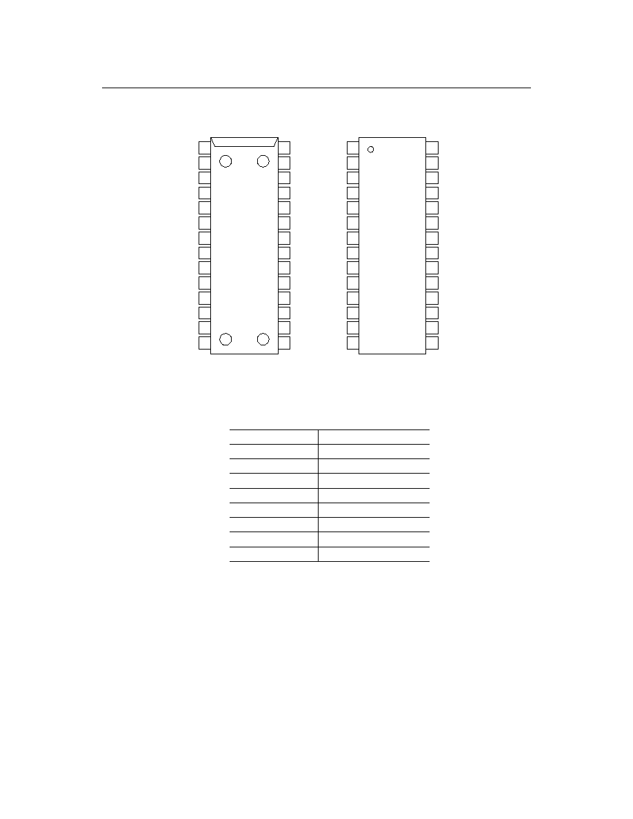
PIN CONFIGURATION (TOP VIEW)
3
4
5
9
10
11
12
13
DQ2
DQ3
DQ4
A10R
A0
A1
A2
A3
26
25
24
20
19
18
17
16
DQ7
DQ6
DQ5
A8
A7
A6
A5
A4
2
DQ1
27 DQ8
1
V
CC
28 V
SS
28-Pin Plastic SOJ
3
4
5
9
10
11
12
13
26
25
24
20
19
18
17
16
2
27
1
28
28-Pin Plastic TSOP
(K Type)
6
WE
23
CAS
23
8
NC
21 A9
21
6
8
7
RAS
22
OE
22
7
14
V
CC
15 V
SS
14
15
DQ2
DQ3
DQ4
A10R
A0
A1
A2
A3
DQ1
V
CC
WE
NC
RAS
V
CC
DQ7
DQ6
DQ5
A8
A7
A6
A5
A4
DQ8
V
SS
CAS
A9
OE
V
SS
Pin Name
Function
A0 - A9, A10R
Address Input
RAS
Row Address Strobe
CAS
Column Address Strobe
DQ1 - DQ8
Data Input/Data Output
OE
Output Enable
WE
Write Enable
V
CC
Power Supply (3.3 V)
V
SS
Ground (0 V)
Note :
The same power supply voltage must be provided to every V
CC
pin, and the same GND
voltage level must be provided to every V
SS
pin.

° Semiconductor
MSM51V17805D/DSL
4/17
ELECTRICAL CHARACTERISTICS
Absolute Maximum Ratings
Recommended Operating Conditions
Capacitance
*: Ta = 25
∞
C
Voltage on Any Pin Relative to V
SS
Short Circuit Output Current
Power Dissipation
Operating Temperature
Storage Temperature
V
T
Symbol
I
OS
P
D
*
T
opr
T
stg
≠0.5 to 4.6
50
1
0 to 70
≠55 to 150
Rating
mA
W
∞C
∞C
Parameter
V
Unit
Power Supply Voltage
Input High Voltage
Input Low Voltage
V
CC
Symbol
V
SS
V
IH
V
IL
3.3
0
--
--
Typ.
Parameter
3.0
0
2.0
≠0.3
Min.
3.6
0
V
CC
+ 0.3
0.8
Max.
(Ta = 0∞C to 70∞C)
V
Unit
V
V
V
Input Capacitance (A0 - A9, A10R)
Input Capacitance (
RAS, CAS, WE, OE)
Output Capacitance (DQ1 - DQ8)
C
IN1
Symbol
C
IN2
C
I/O
5
7
7
Max.
pF
Unit
pF
pF
Parameter
(V
CC
= 3.3 V ±0.3 V, Ta = 25∞C, f = 1 MHz)
--
--
--
Typ.

° Semiconductor
MSM51V17805D/DSL
5/17
DC Characteristics
Parameter
Symbol
Condition
MSM51V17805
D/DSL-50
MSM51V17805
D/DSL-60
MSM51V17805
D/DSL-70
(V
CC
= 3.3 V ±0.3 V, Ta = 0∞C to 70∞C)
I
OH
= ≠2.0 mA
Output High Voltage
I
OL
= 2.0 mA
Output Low Voltage
0 V
£ V
I
£ V
CC
+ 0.3 V;
All other pins not
Input Leakage Current
under test = 0 V
DQ disable
Output Leakage Current
0 V
£ V
O
£ V
CC
RAS, CAS cycling,
Average Power
t
RC
= Min.
Supply Current
(Operating)
RAS, CAS = V
IH
Power Supply
RAS, CAS
Current (Standby)
RAS cycling,
Average Power
CAS = V
IH
,
Supply Current
t
RC
= Min.
(
RAS-only Refresh)
RAS = V
IH
,
Power Supply
CAS = V
IL
,
Current (Standby)
DQ = enable
Average Power
CAS before RAS
Supply Current
(
CAS before RAS Refresh)
Average Power
RAS £ 0.2 V,
Supply Current
CAS £ 0.2 V
(
CAS before RAS
V
OH
V
OL
I
LI
I
LO
I
CC1
I
CC2
I
CC3
I
CC5
I
CC6
I
CCS
V
CC
≠0.2 V
Min.
Max.
Min.
Max.
Min.
Max.
Unit Note
RAS cycling,
2.4
0
≠10
≠10
--
--
--
--
--
--
--
V
CC
0.4
10
10
100
2
0.5
100
100
300
5
2.4
0
≠10
≠10
--
--
--
--
--
--
--
V
CC
0.4
10
10
90
2
0.5
90
90
300
5
2.4
0
≠10
≠10
--
--
--
--
--
--
--
V
CC
0.4
10
10
80
2
0.5
80
80
300
5
--
200
--
200
--
200
V
V
mA
mA
mA
mA
mA
mA
mA
mA
1, 2
1, 2
1, 2
1, 5
1
1
mA 1, 5
t
RC
= 62.5
ms,
Average Power
CAS before RAS,
Supply Current
t
RAS
£ 1 ms
(Battery Backup)
I
CC10
--
300
--
300
--
300
mA
1, 4,
RAS = V
IL
,
Average Power
CAS cycling,
Supply Current
t
HPC
= Min.
(Fast Page Mode)
I
CC7
--
100
--
90
--
80
mA
1, 3
5
Self-Refresh)
Notes : 1. I
CC
Max. is specified as I
CC
for output open condition.
2. The address can be changed once or less while RAS = V
IL
.
3. The address can be changed once or less while CAS = V
IH
.
4. V
CC
≠ 0.2 V £ V
IH
£ V
CC
+ 0.3 V, ≠0.3 V £ V
IL
£ 0.2 V.
5. SL version.