 | –≠–ª–µ–∫—Ç—Ä–æ–Ω–Ω—ã–π –∫–æ–º–ø–æ–Ω–µ–Ω—Ç: MSM5259 | –°–∫–∞—á–∞—Ç—å:  PDF PDF  ZIP ZIP |

MSM5259
° Semiconductor
1/18
GENERAL DESCRIPTION
The MSM5259 is a dot matrix LCD segment driver which is fabricated using low power CMOS
metal gate technology. This LSI consists of 40-bit shift register, 40-bit latch and 40-bit 4-level
driver.
It converts serial data, which is received from an LCD controller LSI, to parallel data and outputs
LCD driving waveforms to LCD.
Expansion of the display can be easily made according to the number and structure of characters.
Since the 40-bit shift register of this device consists of two 20-bit shift registers, it is possible to
allot bits efficiently according to the number of characters.
The MSM5259 can drive a variety of LCD panels because the bias voltage, which determines the
LCD driving voltage, can be optionally supplied from the external source. For static operation
only, the device is available with a power supply voltage of 2.5V or more.
FEATURES
∑ Supply voltage
: 3.5 to 6.0V (Dynamic display)
: 2.5 to 6.0V (Static display)
∑ LCD driving voltage : 2.5 to 6.0V (Static display)
∑ Applicable LCD duty : 1/8 to 1/16
∑ Interface with MSM6222-xx (Dot matrix LCD controller with 16-dot common driver and 40-
dot segment driver)
∑ Bias voltage can be supplied externally.
∑ Package options:
56-pin plastic QFP (QFP56-P-910-0.65-K) (Product name : MSM5259GS-K)
56-pin plastic QFP (QFP56-P-910-0.65-L2) (Product name : MSM5259GS-L2)
56-pin plastic QFP (QFP56-P-910-0.65-2K) (Product name : MSM5259GS-2K)
56-pin plastic QFP (QFP56-P-910-0.65-2L2) (Product name : MSM5259GS-2L2)
° Semiconductor
MSM5259
40-DOT SEGMENT DRIVER
E2B0019-27-Y2
This version: Nov. 1997
Previous version: Mar. 1996
MSM5259
° Semiconductor
2/18
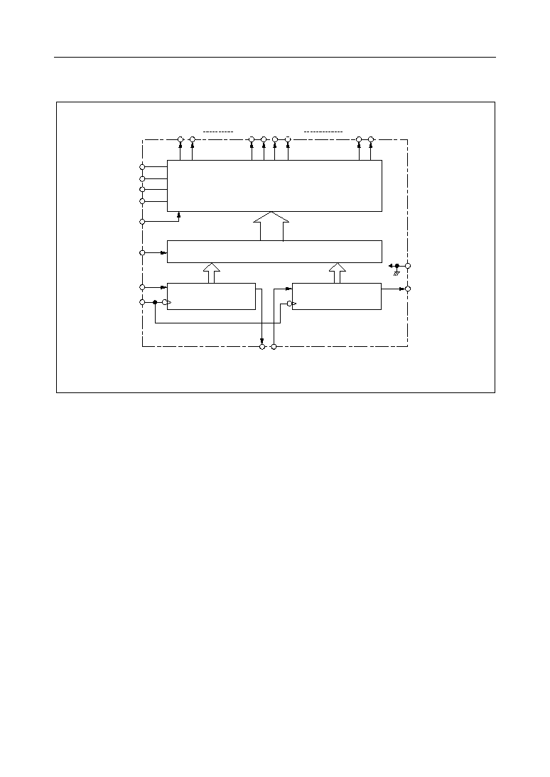
BLOCK DIAGRAM
O
1
O
2
O
19
O
20
O
21
O
22
O
40
O
39
V
DD
V
2
V
3
V
5
DF
LOAD
DI
1
CP
DO
20
DI
21
V
SS
DO
40
40-Bit 4-Level Driver
40-Bit Latch
20-Bit Shift
Register
20-Bit Shift
Register
MSM5259
° Semiconductor
3/18
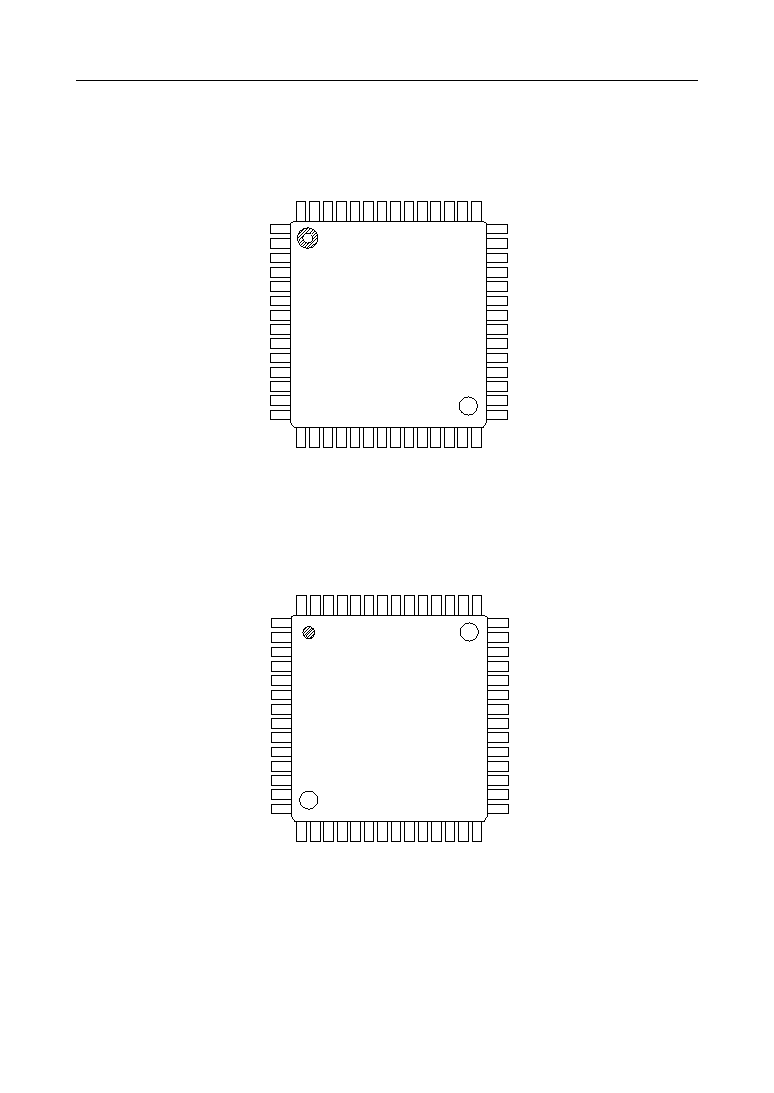
PIN CONFIGURATION
56
55
54
53
52
51
50
49
48
47
46
45
44
43
4
3
2
1
5
6
7
8
9
10
11
12
13
14
15
16
17
18
19
20
21
22
23
24
25
26
27
28
39
40
41
42
38
37
36
35
34
33
32
31
30
29
O
1
DI
21
DO
20
V
5
V
2
LOAD
V
DD
DI
1
DF
NC
NC
NC
O
27
O
26
O
24
O
23
O
21
*(V
DD
)
O
20
O
18
O
17
O
16
O
15
O
2
O
3
O
4
O
5
O
6
O
7
O
8
O
9
O
10
O
11
DO
40
O
40
O
39
O
38
O
37
O
36
O
35
O
34
O
33
O
32
O
31
O
12
O
30
O
13
O
29
O
14
O
28
O
19
O
22
O
25
V
SS
V
3
CP
(Top View)
1
2
3
4
5
6
7
8
9
10
11
12
13
14
53
54
55
56
52
51
50
49
48
47
46
45
44
43
42
41
40
39
38
37
36
35
34
33
32
31
30
29
18
17
16
15
19
20
21
22
23
24
25
26
27
28
NC
O
14
O
13
O
12
O
10
O
5
O
8
O
6
O
4
O
3
O
2
O
1
O
28
O
29
O
31
O
32
O
34
O
35
O
36
O
38
O
39
O
40
DO
40
NC
NC
DF
LOAD
DI
CP
V
DD
V
SS
V
2
V
3
O
15
O
16
O
17
O
18
O
19
O
20
*(V
DD
)
O
21
O
22
O
23
O
24
V
5
O
25
DO
20
O
26
DI
21
O
27
O
37
O
33
O
30
O
9
O
11
O
7
NC : No connection
56-Pin Plastic QFP (Type L)
NC : No connection
56-Pin Plastic QFP (Type K)
*
Do not connect pin 21 to the other signal pins, because the pin is internally connected to V
DD
.
Do not use pin 21 as a single V
DD
signal line. It is permissible to use pin 21 for supplying a
higher power of V
DD
.
Note : The figure for Type L shows the configuration viewed from the reverse side of the package.
Pay attention to the difference in pin arrangement.
MSM5259
° Semiconductor
4/18
ABSOLUTE MAXIMUM RATINGS
Parameter
Supply Voltage (1)
Symbol
Condition
Rating
Unit
V
DD
≠0.3 to +6.5
V
Supply Voltage (2)
V
DD ≠
V
5
Ta = 25∞C
0 to +6.5
V
Input Voltage
V
I
≠0.3 to V
DD
+0.3
V
Storage Temperature
T
STG
--
≠55 to +150
∞C
*1
RECOMMENDED OPERATING CONDITIONS
Parameter
Supply Voltage (1)
Symbol
Condition
Rnage
Unit
V
DD
3.5 to 6.0
V
Static
2.5 to 6.0
Supply Voltage (2)
V
DD ≠
V
5
2.5 to 6.0
V
Operating Temperature
Top
--
≠30 to +85
∞C
Dynamic
--
*1
*2
*1 V
DD
> V
2
> V
3
> V
5
> V
SS
(Dynamic display)
V
DD
= V
3
> V
2
= V
5
= V
SS
(Static display)
For V
DD
of less than 3.5V, the device is available only for static operation.
*2 V
DD
is the reference potential for the LCD driving voltage.
To determine the LCD driving voltage, change the value of V
5
. (0V Minimum)
MSM5259
° Semiconductor
5/18
ELECTRICAL CHARACTERISTICS
DC Characteristics (1)
2
3
1
3
Parameter
"H" Input Voltage
Symbol
Condition
Min.
Typ.
Max.
Unit
V
IH
--
0.8V
DD
--
V
DD
V
"L" Input Voltage
V
IL
--
0
--
0.2V
DD
V
"H" Input Current
I
IH
V
IH
= V
DD
--
--
1
m
A
"L" Input Current
I
IL
V
IL
= 0V
--
--
≠1
m
A
"H" Output Voltage
V
OH
I
O
= ≠40mA
4.2
--
--
V
"L" Output Voltage
V
OL
I
O
= 0.4mA
--
--
0.4
V
ON Resistance
R
ON
V
DD
≠V
5
= 5V
|V
N
≠V
O
|
= 0.25V
--
--
5
kW
Supply Current
I
DD
f
CP
= 0Hz, No load
--
--
0.5
mA
*1
*1
*1
*1
*2
*2
*3
*4
(V
DD
= 5V±10%, Ta=≠30 to +85∞C)
*1 Applicable to DF, LOAD, DI
1
and DI
21
.
*2 Applicable to DO
20
and DO
40
.
*3 Applicable to O
1
to O
40
.
*4 Dynamic display : V
N
= V
DD
to V
5
, V
2
= (V
DD
≠ V
5
), V
3
= (V
DD
≠ V
5
)
Static display : V
N
= V
DD
to V
5
, V
3
= V
DD
, V
2
= V
5
= V
SS
DC Characteristics (2)
(Only for static operation)
Parameter
"H" Input Voltage
Symbol
Condition
Min.
Typ.
Max.
Unit
V
IH
--
0.8V
DD
--
V
DD
V
"L" Input Voltage
V
IL
--
0
--
0.2V
DD
V
"H" Input Current
I
IH
V
IH
= V
DD
--
--
1
m
A
"L" Input Current
I
IL
V
IL
= 0V
--
--
≠1
m
A
"H" Output Voltage
V
OH
I
O
= ≠40mA
2.2
--
--
V
"L" Output Voltage
V
OL
I
O
= 0.2mA
--
--
0.4
V
ON Resistance
R
ON
V
3
= V
DD
= 3V, V
2
= V
5
= V
SS
= 0V,
| V
N
≠V
O
| = 0.25V
--
--
10
kW
Supply Current
I
DD
f
CP
= 0Hz, No load
--
--
0.5
mA
*1
*1
*1
*1
*5
*5
*6
(V
DD
= 3V±0.5V, Ta=≠30 to +85∞C)
*5 Applied to DO
20
and DO
40
.
*6 Applied to O
1
to O
40
.
MSM5259
° Semiconductor
6/18
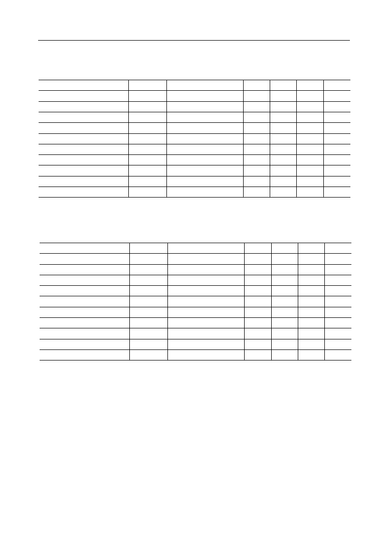
Switching Characteristics (1)
Parameter
"H", "L" Propagation Delay Time
Symbol
Condition
Min.
Typ.
Max.
Unit
t
PLH,
t
PHL
--
--
--
250
ns
Clock Frequency
f
CP
Duty = 50%
--
--
3.3
MHz
Clock Pulse Width
t
W (CP)
125
--
--
ns
Load Pulse Width
t
W (L)
125
--
--
ns
Data Set-up Time DI
∆
CP
t
SETUP
50
--
--
ns
Data Hold Time DI
∆
CP
t
HOLD
50
--
--
ns
(V
DD
= 5V±10%, Ta=≠30 to +85∞C, C
L
=15pF)
CP ∆ LOAD Set-up Time
t
CL
250
--
--
ns
LOAD ∆ CP Hold Time
t
LC
0
--
--
ns
CP Rise/Fall Time
t
r(CP)
, t
f(CP)
--
--
50
ns
LOAD Rise/Fall Time
t
r(L)
, t
f(L)
--
--
1
m
s
--
--
--
--
--
--
--
--
Switching Characteristics (2)
Parameter
"H", "L" Propagation Delay Time
Symbol
Condition
Min.
Typ.
Max.
Unit
t
PLH,
t
PHL
--
--
--
800
ns
Clock Frequency
f
CP
Duty = 50%
--
--
1.0
MHz
Clock Pulse Width
t
W (CP)
300
--
--
ns
Load Pulse Width
t
W (L)
300
--
--
ns
DI ∆ CP Set-up Time
t
SETUP
200
--
--
ns
DI ∆ CP Hold Time
t
HOLD
200
--
--
ns
(V
DD
= 3V±0.5V, Ta=≠30 to +85∞C, C
L
=15pF)
CP ∆ LOAD Set-up Time
t
CL
800
--
--
ns
LOAD ∆ CP Hold Time
t
LC
0
--
--
ns
CP Rise/Fall Time
t
r(CP)
--
--
1
m
s
LOAD Rise/Fall Time
t
r(L)
, t
f(L)
--
--
1
m
s
--
--
--
--
--
--
--
--
(Only for static operation)
MSM5259
° Semiconductor
7/18
CP
DI
21
DO
40
LOAD
0.8V
DD
t
w
(CP)
0.8V
DD
t
f
(CP)
t
w
(CP)
0.2V
DD
t
r
(CP)
0.8V
DD
0.2V
DD
0.8V
DD
0.2V
DD
0.8V
DD
0.8V
DD
0.2V
DD
0.2V
DD
0.8
0.8
V
DD
V
DD
0.2
0.2
V
DD
V
DD
t
HOLD
t
SETUP
t
HOLD
t
SETUP
0.8V
DD
0.2V
DD
t
PLH
t
PHL
t
CL
0.2V
DD
0.2V
DD
t
LC
t
w
(L)
t
r
(L)
t
f
(L)
DI
1
DO
20
0.8V
DD
0.8V
DD
MSM5259
° Semiconductor
8/18
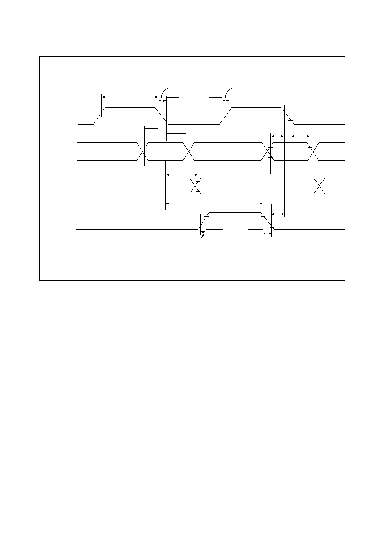
TIMING DIAGRAM
1/5 bias, 1/16 duty
Frame
signal
LOAD
LATCH
DATA
DF
DF
LOAD
DI
CP
LATCH
DATA
LOAD
LATCH
DATA
DF
V
DD
V
a
V
b
V
c
V
d
V
e
V
LCD
16
1
2
3
16
1
2
3
H
L
H
H
H
H
L
L
L
V
2
V
DD
V
3
V
5
R
R
R
R
R
VR
V
DD
V
a
V
b
V
c
V
d
V
e
V
LCD
V
a
= V
DD
≠ V
LCD
5
1
≠
V
b
= V
DD
≠ V
LCD
5
2
≠
V
c
= V
DD
≠ V
LCD
5
3
≠
V
d
= V
DD
≠ V
LCD
5
4
≠
V
e
= V
DD
≠ V
LCD
V
LCD
= LCD driving voltage
V
ss
MSM5259
MSM5259
° Semiconductor
9/18
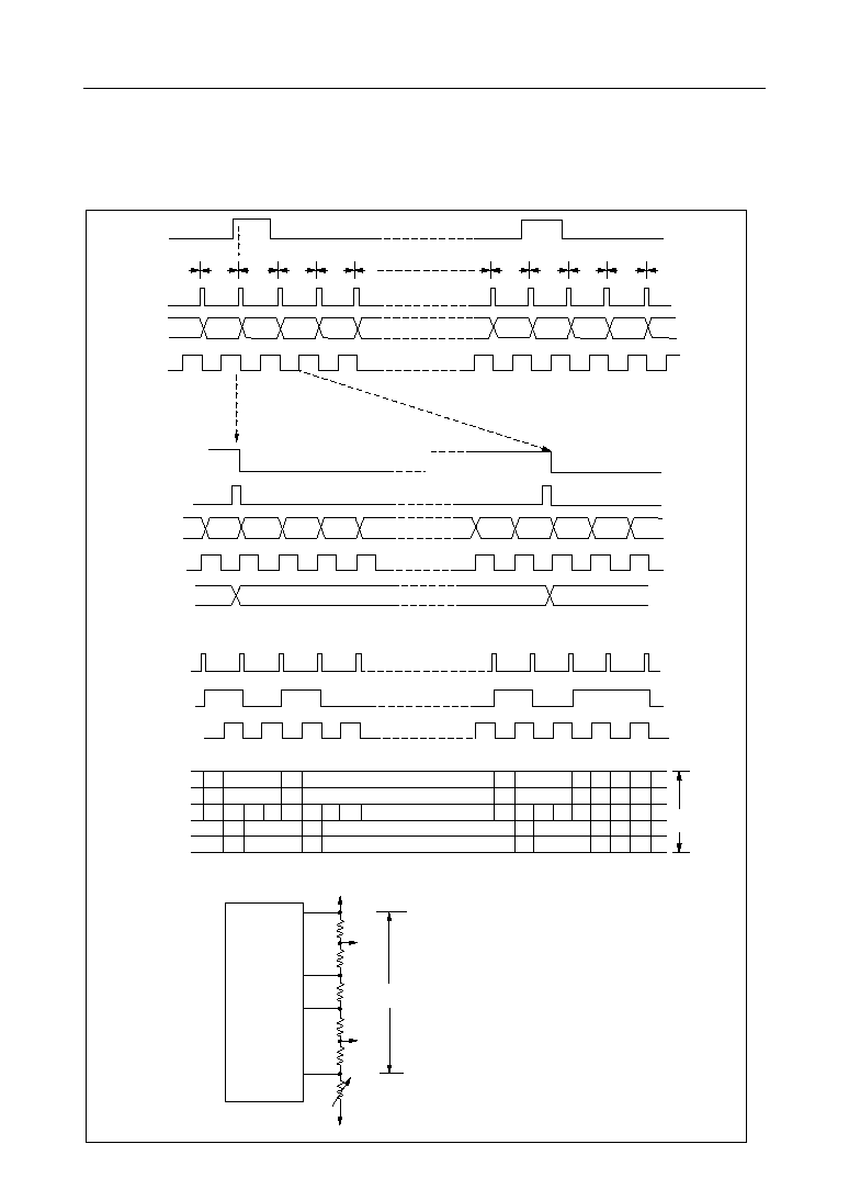
Static Display
V
DD
V
DD
V
3
V
5
V
SS
V
2
O
40
DF
O
1
Bias supply pin
Common signal
V
DD
V
SS
DF
Output (lighting on)
Output (lighting off)
V
DD
, V
3
V
SS
, V
5
, V
2
V
DD
, V
3
V
SS
, V
5
, V
2

MSM5259
° Semiconductor
10/18
FUNCTIONAL DESCRIPTION
Pin Functional Description
∑ DI
1
The data (1st to 20th bit) from the LCD controller LSI is input to 20-bit shift register from DI
1
.
(Positive logic)
∑ DI
21
Data input to the shift register (21st to 41st bit).
Connecting DO
20
and DI
21
allows configuration of a 40-bit register.
If DI
21
is not used, connect this pin to V
SS
.
∑ CP
Clock pulse input pin for the two 20-bit shift registers. The data is input to the 20-bit shift
register at the falling edge of the clock pulse. A data set up time (t
SETUP
) and data hold time
(t
HOLD
) are required between the DI1 and DI21 signals and a clock pulse.
∑ DO
20
20th bit of the shift register contents is output from DO
20
. The data which was input from DI
1
is output from this pin with a delay of the number of bits of the shift register (20), synchronized
with the clock pulse. By connecting DO
20
to DI
21
, two 20-bit shift registers can be used as a
40-bit shift register.
∑ DO
40
40th bit of the shift register contents is output from DO
40
. The data which was input from DI
21
is output from this pin with a delay of the number of bits of the shift register (20), synchronized
with the clock pulse. By connecting DO
40
to the next MSM5259's DI
1
, this LSI is applicable
to a wide screen LCD.
Refer to the application circuit.
∑ DF
Alternate signal input pin for LCD driving.
∑ LOAD
Signal for latching the shift register contents is input from this pin. When the LOAD pin is
set at "H" level, the shift register contents are transferred to the 40-bit 4-level driver. When
LOAD pin is set at "L" level, the last display output data (O
1
- O
40
), which was transferred
when LOAD pin was at "H" level, is held.
∑ V
DD
, V
SS
Supply voltage pins.
V
DD
is generally set to 4.0 to 6.0V. V
SS
is a ground pin (V
SS
= 0V)
∑ V
2
, V
3
, V
5
Bias supply voltage pins to drive the LCD. Bias voltage divided by the register is usually used
as supply voltage source.
Refer to the application circuit.
For static operation, connect V
3
to V
DD
and also connect V
2
, V
5
, to V
SS
.
MSM5259
° Semiconductor
11/18
Latched data
DF
Driver output level
"H"
(Select)
H
V
5
L
V
DD
"L"
(Non-select)
H
V
3
L
V
2
∑ O
1
to O
40
Display data output pin which corresponds to each data bit in the latch. One of V
DD
, V
2
, V
3
and V
5
is selected as a display driving voltage source according to the combination of latched
data level and DF signal. (Refer to the truth table below.)
Truth Table
MSM5259
° Semiconductor
12/18
Common
O
1
O
2
O
3
O
4
O
5
O
6
O
7
O
8
O
9
O
10
O
11
O
12
O
13
O
14
O
15
O
16
V
DD
V
a
V
b
V
c
V
d
V
e
O
1
O
2
O
1
O
2
V
DD
V
a
V
b
V
c
V
d
V
e
O
1
O
2
O
3
O
4
O
5
Segment
V
a
= V
DD
≠ V
LCD
5
1
≠
V
b
= V
DD
≠ V
LCD
5
2
≠
V
c
= V
DD
≠ V
LCD
5
3
≠
V
d
= V
DD
≠ V
LCD
5
4
≠
V
e
= V
DD
≠ V
LCD
V
LCD
V
LCD
5
3
≠
V
LCD
5
1
≠
O
≠V
LCD
≠
V
LCD
5
1
≠
≠
V
LCD
5
3
≠
V
DD
V
a
V
b
V
c
V
d
V
e
V
DD
V
a
V
b
V
c
V
d
V
e
V
LCD
V
LCD
5
1
≠
O
≠V
LCD
≠
V
LCD
5
1
≠
Common O
1
-Segment O
1
(Select waveform)
Common O
2
-Segment O
1
(Non-select waveform)
1 frame
V
LCD
1
2
3
4
16
1
LCD Driving Waveform (1/5 bias, 1/16 duty)
MSM5259
° Semiconductor
13/18
APPLICATION CIRCUITS
(Connected to MSM6222B-01 LCD Controller)
LCD
COM 1-16
SEG 1-40
DO
MSM6222B-01
MSM5259
V
DD
V
SS
V
2
V
3
V
5
CP
L
DF
V
DD
GND
V
1
V
2
V
3
V
4
V
5
O
1
-O
40
DF
CP
LOAD
DI
1
DO
20
DI
21
DO
40
MSM5259
V
DD
V
SS
V
2
V
3
V
5
O
1
-O
40
DF
CP
LOAD
DI
1
DO
20
DI
21
DO
40
MSM5259
V
DD
V
SS
V
2
V
3
V
5
O
1
-O
40
DF
CP
LOAD
DI
1
DO
20
DI
21
DO
40
C
C
C
C
C
OV
R
R
R
R
R
+5V
MSM5259
° Semiconductor
14/18
Application Circuit for Static Display
V
5
V
3
V
DD
V
2
O
1
CP
DI
1
DF
LOAD
V
SS
(GND)
COM
COM
MSM4069
32-120H
Z
Duty 50%
COMMON
SIGNAL
DATA IN
SHIFT
CLOCK
LOAD
DO
20
DI
21
MSM5259
O
40
DO
40
+5V
V
5
V
3
V
DD
V
2
O
1
CP
DI
1
DF
LOAD
V
SS
(GND)
DO
20
DI
21
MSM5259
O
40
+5V
80-DOT LCD PANEL
Seg
40
Seg
1
Seg
80
Seg
41
The MSM5259 is applicable to a static LCD by setting V
2
and V
5
at ground level, connecting V
3
to V
DD
and
inputting COMMON SIGNAL to DF pin.
This sample application circuit below is the case when the MSM5259 is applied to an 80-bit LCD panel by connecting
two MSM5259s in series.
MSM5259
° Semiconductor
15/18
(Unit : mm)
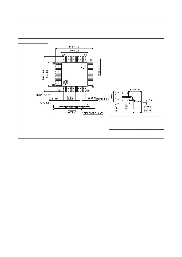
PACKAGE DIMENSIONS
Notes for Mounting the Surface Mount Type Package
The SOP, QFP, TSOP, SOJ, QFJ (PLCC), SHP and BGA are surface mount type packages, which
are very susceptible to heat in reflow mounting and humidity absorbed in storage.
Therefore, before you perform reflow mounting, contact Oki's responsible sales person for the
product name, package name, pin number, package code and desired mounting conditions
(reflow method, temperature and times).
QFP56-P-910-0.65-K
Package material
Lead frame material
Pin treatment
Solder plate thickness
Package weight (g)
Epoxy resin
42 alloy
Solder plating
5 mm or more
0.36 TYP.
Mirror finish

MSM5259
° Semiconductor
16/18
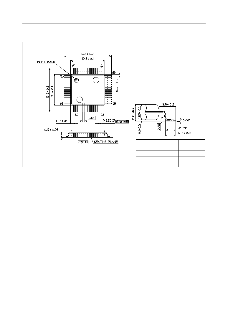
(Unit : mm)
Notes for Mounting the Surface Mount Type Package
The SOP, QFP, TSOP, SOJ, QFJ (PLCC), SHP and BGA are surface mount type packages, which
are very susceptible to heat in reflow mounting and humidity absorbed in storage.
Therefore, before you perform reflow mounting, contact Oki's responsible sales person for the
product name, package name, pin number, package code and desired mounting conditions
(reflow method, temperature and times).
QFP56-P-910-0.65-L2
Package material
Lead frame material
Pin treatment
Solder plate thickness
Package weight (g)
Epoxy resin
42 alloy
Solder plating
5 mm or more
0.36 TYP.
Spherical surface

MSM5259
° Semiconductor
17/18
(Unit : mm)
Notes for Mounting the Surface Mount Type Package
The SOP, QFP, TSOP, SOJ, QFJ (PLCC), SHP and BGA are surface mount type packages, which
are very susceptible to heat in reflow mounting and humidity absorbed in storage.
Therefore, before you perform reflow mounting, contact Oki's responsible sales person for the
product name, package name, pin number, package code and desired mounting conditions
(reflow method, temperature and times).
QFP56-P-910-0.65-2K
Package material
Lead frame material
Pin treatment
Solder plate thickness
Package weight (g)
Epoxy resin
42 alloy
Solder plating
5 mm or more
0.43 TYP.
Mirror finish
MSM5259
° Semiconductor
18/18
(Unit : mm)
Notes for Mounting the Surface Mount Type Package
The SOP, QFP, TSOP, SOJ, QFJ (PLCC), SHP and BGA are surface mount type packages, which
are very susceptible to heat in reflow mounting and humidity absorbed in storage.
Therefore, before you perform reflow mounting, contact Oki's responsible sales person for the
product name, package name, pin number, package code and desired mounting conditions
(reflow method, temperature and times).
QFP56-P-910-0.65-2L2
Package material
Lead frame material
Pin treatment
Solder plate thickness
Package weight (g)
Epoxy resin
42 alloy
Solder plating
5 mm or more
0.43 TYP.
Spherical surface