MSM5265
° Semiconductor
1/18
° Semiconductor
MSM5265
80-DOT LCD DRIVER
E2B0008-27-Y2
GENERAL DESCRIPTION
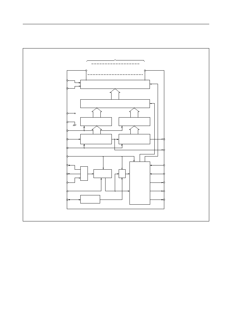
The MSM5265 is an LCD driver which can directly drive up to 80 segments in the static display
mode and up to 160 segments in the 1/2 duty dynamic display mode.
The MSM5265 is fabricated with low power CMOS metal gate technology. The MSM5265
consists of a 160-stage shift register, 160-bit data latch, 80 pairs of LCD drivers and a common
signal generator.
The display data is serially input from the DATA-IN pin to the 160-stage shift register synchronized
with the CLOCK pulse. The data is shifted into the 160-bit data latch by the LOAD signal. Then
the latched data is directly output to the LCD from the 80 pairs of LCD drivers as a serial output.
The common signal can be generated by the built-in generator, or externally input. The common
synchronization circuit which is used in the dynamic display mode is integrated on the chip.
FEATURES
∑ Supply voltage : 3.0 to 6.0 V
∑ Drives LCD of up to 80 segments (in the static display mode)
∑ Drives LCD of up to 160 segments (in the 1/2 duty dynamic display mode)
∑ Simple interface with microcomputer
∑ Bit-to-bit correspondence between input data and output data
H: Display ON
L: Display OFF
∑ Can be cascade-connected
∑ Built-in common signal generator
∑ Can be synchronized with the external common signal
∑ Testing pins for all-on (SEG-TEST) and all-off (BLANK)
∑ Applicable as an output expander
∑ LCD driving voltage can be adjusted by the combination of V
LC1
and V
LC2
∑ Package options:
100-pin plastic QFP (QFP100-P-1420-0.65-K) (Product name : MSM5265GS-K)
100-pin plastic QFP (QFP100-P-1420-0.65-BK) (Product name : MSM5265GS-BK)
This version: Nov. 1997
Previous version: Mar. 1996
MSM5265
° Semiconductor
3/18
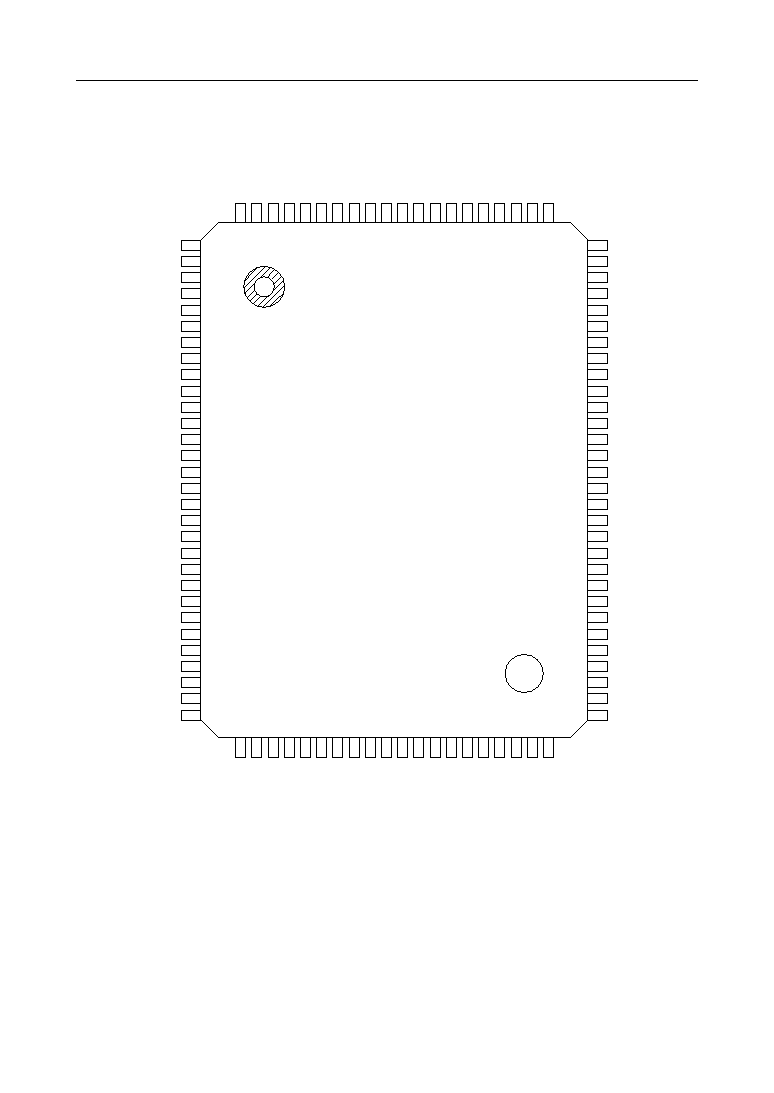
PIN CONFIGURATION (TOP VIEW)
50
1
2
3
4
5
6
7
8
9
10
11
12
13
14
15
16
17
18
19
20
21
22
23
24
25
26
27
28
29
30
SEG51
SEG52
SEG53
SEG54
SEG55
SEG56
SEG57
SEG58
SEG59
SEG60
SEG61
SEG62
SEG63
SEG64
SEG65
SEG66
SEG67
SEG68
SEG69
SEG70
SEG71
SEG72
SEG73
SEG74
SEG75
SEG76
SEG77
SEG78
SEG79
SEG80
49
48
47
46
45
44
43
42
41
40
39
38
37
36
35
34
33
32
31
V
LC2
COM-B
COM-A
V
LC1
COM-OUT
SYNC
BLANK
SEG-TEST
GND
D/S
V
DD
EXT/INT
OSC-IN
OSC-OUT
OSC-OUT
DATA-OUT2
DATA-OUT1
DATA-IN
CLOCK
LOAD
80
79
78
77
76
75
74
73
72
71
70
69
68
67
66
65
64
63
62
61
60
59
58
57
56
55
54
53
52
51
SEG30
SEG29
SEG28
SEG27
SEG26
SEG25
SEG24
SEG23
SEG22
SEG21
SEG20
SEG19
SEG18
SEG17
SEG16
SEG15
SEG14
SEG13
SEG12
SEG11
SEG10
SEG9
SEG8
SEG7
SEG6
SEG5
SEG4
SEG3
SEG2
SEG1
SEG31
SEG32
SEG33
SEG34
SEG35
SEG36
SEG37
SEG38
SEG39
SEG40
SEG41
SEG42
SEG43
SEG44
SEG45
SEG46
SEG47
SEG48
SEG49
SEG50
81
82
83
84
85
86
87
88
89
90
91
92
93
94
95
96
97
98
99
100
100-Pin Plastic QFP
MSM5265
° Semiconductor
5/18
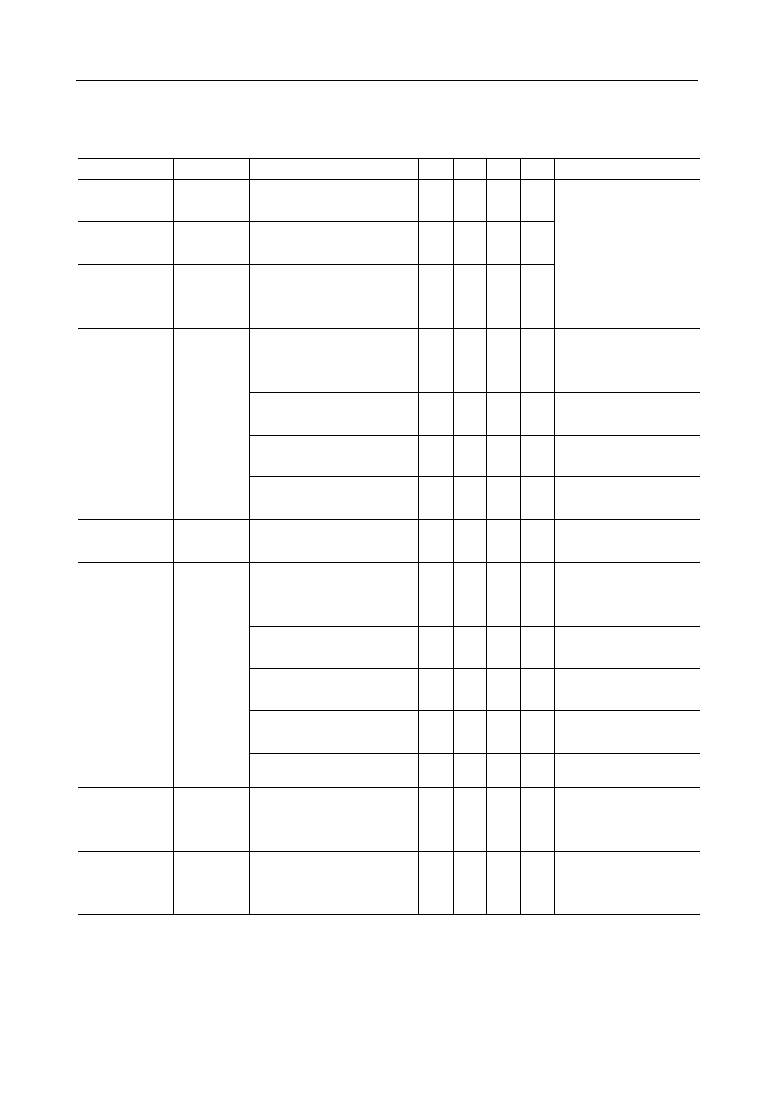
ELECTRICAL CHARACTERISTICS
DC Characteristics
Parameter
Symbol
Condition
Applicable pin
Min. Typ. Max. Unit
"H" Input
Voltage
"L" Input
Voltage
Input
Leakage
Current
V
IH
V
IL
I
IL
--
--
V
I
= 5.0 V/0 V
36
--
V
DD
V
GND
--
1.0
V
--
--
±1
mA
SEG-TEST, BLANK,
LOAD, DATA-IN, CLOCK,
D/S, EXT/INT, OSC-IN
"H" Output
Voltage
V
OH
I
O
= ≠100 mA
4.5
--
--
V
DATA-OUT1
DATA-OUT2
COM-OUT
V
LC1
= 2.5 V, V
LC2
= 0 V
I
O
= ≠30 mA
4.8
--
--
V
OSC-OUT
OSC-OUT
SEG
1
-SEG
80
V
LC1
= 2.5 V, V
LC2
= 0 V
I
O
= ≠150 mA
4.8
--
--
V
COM-A
COM-B
"M" Output
Voltage
V
OM
V
LC1
= 2.5 V, V
LC2
= 0 V
I
O
= ±150 mA
2.3
--
2.7
V
COM-A
COM-B
DATA-OUT1
DATA-OUT2
COM-OUT
"L" Output
Voltage
V
OL
I
O
= 100 mA
--
--
0.5
V
I
O
= ≠200 mA
4.5
--
--
V
OSC-OUT
OSC-OUT
I
O
= 200 mA
--
--
0.5
V
V
LC1
= 2.5 V, V
LC2
= 0 V
I
O
= 30 mA
--
--
0.2
V
SEG
1
- SEG
80
V
LC1
= 2.5 V, V
LC2
= 0 V
I
O
= 150 mA
--
--
0.2
V
COM-A
COM-B
I
O
= 250 mA
--
--
0.8
V
SYNC
Output
Leakage
Current
Segment
Output
Impedance
I
LO
V
O
= 5 V
when internal Tr is off
--
--
5
mA
SEG
1
- SEG
80
R
SEG
V
LC1
= (5+V
LC2
)/2
V
LC2
= 0 to 2 V
--
--
10
kW
SYNC
(V
DD
= 5.0 V Ta =≠40 to +85∞C)