Semiconductor
1
524,288-Words x 16-bit or 1,048,576-Bytes x 8-bit MaskROM
8Words x 16-Bit or 16Bytes x 8-Bit/Page Mode MASKROM
DESCRIPTION
FEATURES
Pin compatible OTP available
Packages:
42-PIN PLASTIC DIP
44-PIN PLASTIC SOP
44-PIN PLASTIC TSOP
Internal powerdown function
Tri-State output configurations
Input/Output TTL compatible
Access time
100ns Max (Normal access)
50ns Max (Page access)
524,288-words x 16-bit / 1,048,576-Bytes x 8-bit
Single 5.0V power supply
The OKI MSM538052E is a 524,288-words x 16-bit or 1,048,576-Bytes x 8-bit CMOS Mask
ROM with an asynchronous page read mode. Each page is organized 8 words x 16-bit or 16
words x 8-bit. It operates on a single 5.0V power supply and is TTL compatible. The chip's
asynchronous I/O requires no external clock assuring easy operation. A power-down mode
provides low power dissipation when the chip is not selected. The CE and OE pins are
provided as control signals that permit three-stated output allowing easy memory expansion
on a system bus.The MSM538052E is suited for use as large capacity fixed memory for
microcomputers and data terminals.
MSM538052E
8-words(A2,A1,A0) or 16-Bytes(A2,A1,A0,A-1) / Page
(DIP42-P-600-2.54)
(SOP44-P-600-1.27-K)
(TSOP44-P-400-0.80-1K)
(MSM538052E-xxRS)
(MSM538052E-xxGS-K)
(MSM538052E-xxTS-AK)
1998.10
MSM538052E
2
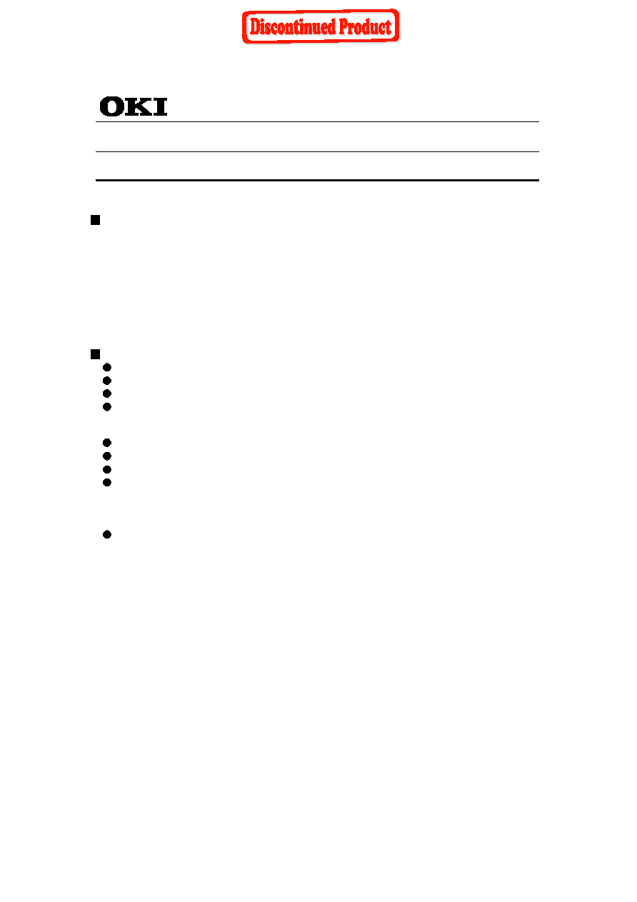
PIN CONFIGURATION
BYTE
2
3
4
5
6
7
8
9
10
11
12
13
14
15
16
17
41
40
39
38
37
36
35
34
33
32
31
30
29
28
A17
A7
A6
A5
A4
A3
A2
A1
A0
CE
V
SS
OE
D0
D8
D1
A8
A9
A10
A11
A12
A13
A14
A15
A16
V
SS
D15/A-1
D7
D14
D6
42PIN DIP
18
27
D9
D13
19
26
D2
D5
20
21
25
24
D10
D3
D12
D4
23
D11
V
CC
22
42
1
A18
NC
BYTE
3
4
5
6
7
8
9
10
11
12
13
14
15
16
17
18
42
41
40
39
38
37
36
35
34
33
32
31
30
29
A17
A7
A6
A5
A4
A3
A2
A1
A0
CE
V
SS
OE
D0
D8
D1
A8
A9
A10
A11
A12
A13
A14
A15
A16
V
SS
D15/A-1
D7
D14
D6
44PIN SOP/
TSOP
19
28
D9
D13
20
27
D2
D5
21
22
26
25
D10
D3
D12
D4
24
D11
V
CC
23
43
1
2
44
NC
A18
NC
NC
Pin Name
Function
D15/A-1
Data output / address input
A0 to A18
Address input
D0 to D15
Data output
CE
OE
Output enable
BYTE
Mode switch
V
CC
, V
SS
Power supply
Chip enable

MSM538052E
3
A0
A1
A2
A3
A4
A5
A6
A7
A8
A9
A10
A11
A12
A13
A14
A15
A16
A17
A18
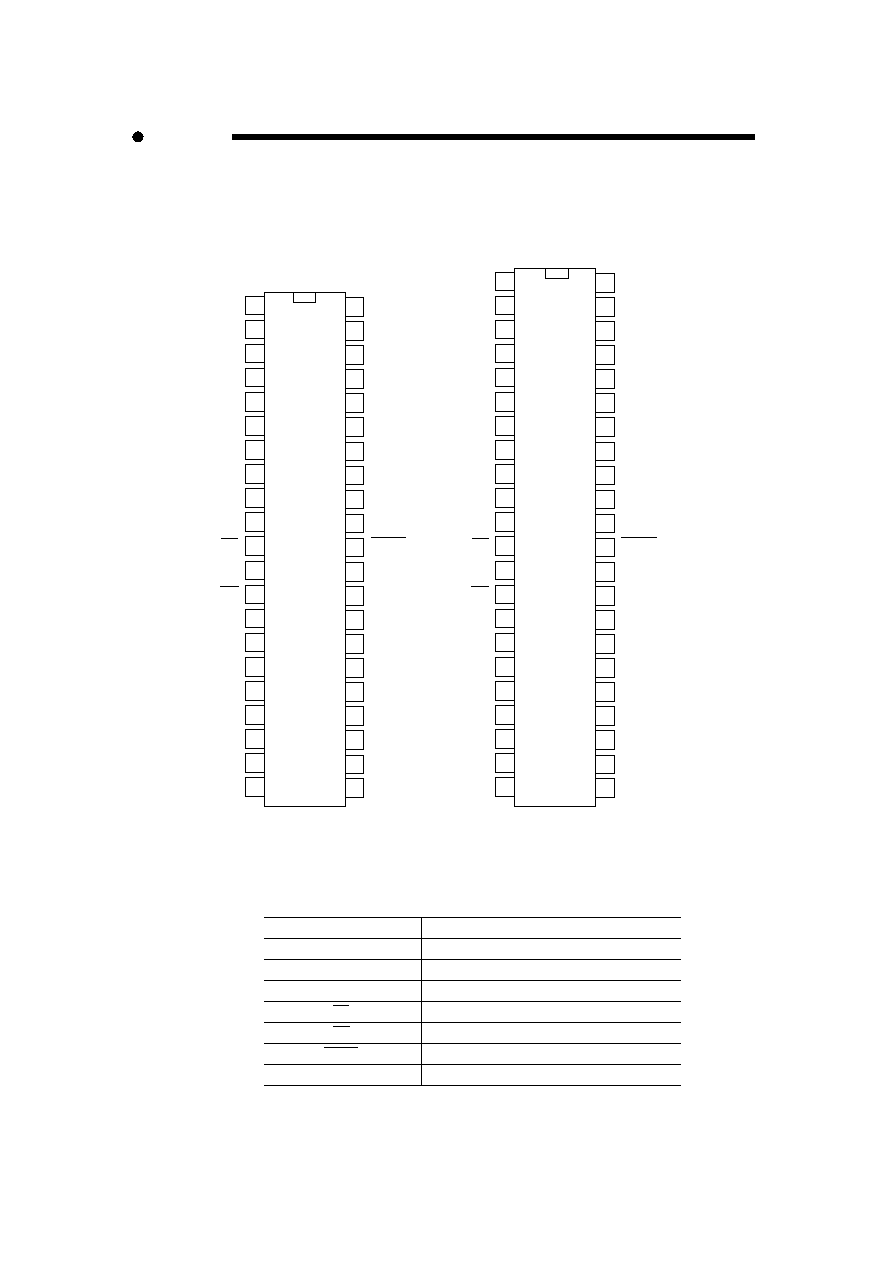
BLOCK DIAGRAM
CE
OE
CE
Control
OE
Address
Buffer
Memory Cell
Matrix
524,288 x 16 or 1,048,676 x 8
FUNCTION TABLE
Output Switching Between 8 and 16 bits
A-1
BYTE
CE
H
MSB
L
L
L
L
OE
X
H
L
L
L
BYTE
X
X
H
L
L
Input Inhibited (D15)
D8 to D15
LSB
DOUT Mode
D8--D15
D0--D7
A-1/D15
X
X
L
H
D0 to D7
D0 to D7
Hi-Z
Hi-Z
Hi-Z
Hi-Z
D8 to D15
Hi-Z
Hi-Z
Hi-Z
16 bit
8 bit
--
A0
A-1
--
A18
A18
V
CC
V
SS
L
L
H
Input Inhibited (D15)
D0 to D7
D8 to D15
16 bit(Page Mode)
A0
A2
L
L
L
L
L
L
D8 to D15
L
H
D0 to D7
Hi-Z
Hi-Z
8 bit(Page Mode)
A-1
A2
X
Decoder
Y
Decoder
Multiplexer & Page Data Latch
Output Buffer
D0
D1
D2
D3
D4
D5
D6
D7
D8
D9
D10
D11
D12
D13
D14
D15

MSM538052E
4
RECOMMENDED OPERATING CONDITIONS
ABSOLUTE MAXIMUM LIMITS
DC CHARACTERISTICS
Operating Temperature
Storage Temperature
Power Supply Voltage
Input Voltage
Output Voltage
Power Dissipation
Parameter
Symbol
Unit
Limits
Conditions
V
V
V
W
�0.3 to 7
�0.3 to V
CC
+ 0.5
�0.3 to V
CC
+ 0.5
0 to 70
�55 to 150
1.0
�C
�C
Per Package T
opr
= 25�C
to V
SS
T
opr
T
stg
V
CC
V
I
V
O
P
D
--
--
Power Supply Voltage
"H" Input Voltage
"L" Input Voltage
Parameter
Symbol
Unit
5.5
Typ.
4.5
Conditions
Min.
Max.
5.0
V
0.0
0.0
0.0
V
2.2
5.0
V
0.8
0.0
V
Operating Temperature
70
0
Limits
--
--
--
--
--
�0.3
--
�C
V
CC
V
SS
V
IH
V
IL
T
opr
"H" Output Voltage
"L" Output Voltage
Parameter
Symbol
Unit
Typ.
2.4
Conditions
Min.
Max.
Power Supply Current
(Operating)
V
0.4
V
10
�A
80
mA
50
�A
500
�A
Input Leakage Current
Output Leakage Current
Power Supply Current
(Standby)
10
�A
Limits
(V
CC
= 5V�10%, Ta = 0 to 70�C)
I
OH
= �400�A
I
OH
= 2.1mA
�10
�10
--
--
--
--
--
--
--
--
--
--
--
--
CE = V
CC
�0.2V
CE = V
IH MIN
V
I
= 0 to V
CC
V
O
= 0 to V
CC
CE = V
IH MIN
CE = V
IL,
OE = V
IH,
t
C
= 100ns
V
OH
I
LI
I
LO
I
CC
I
CCS
I
CCS1
V
OL
5.5
MSM538052E
5
Address
t
C
OE
D
OUT
t
ACC
t
OE
t
OH
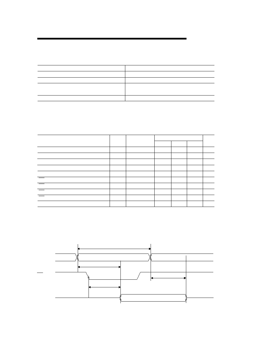
AC CHARACTERISTICS
Test conditions
Parameter
Conditions
Input Signal Level
Transtion Time
Timing Reference Level
Load Condition
V
IH
=3.0V, V
IL
=0.0V
tr=tf=5ns
Input Voltage=1.5V
Output Voltage=0.8V&2.0V
CL=100pF+1TTL
Random Access Cycle time
Parameter
Symbol
Unit
Typ.
100
Conditions
Min.
Max.
ns
100
50
40
0
30
0
0
Read Cycle
Random Address Access time
Page Set up time
OE Access time
CE Output Disable time
OE Output Disable time
Output Hold time
ns
ns
ns
ns
ns
ns
Limits
(Ta = 0 to 70�C)
--
--
--
--
--
--
--
--
--
120
--
--
--
--
--
--
--
--
--
t
C
t
ACC
t
PSET
t
OE
t
CHZ
t
OHZ
t
OH
Page Access Cycle time
50
ns
50
100
Page Access time
CE Access time
ns
ns
--
--
--
--
--
--
--
--
--
t
PC
t
PAC
t
CE
--
Read Cycle (Note1)
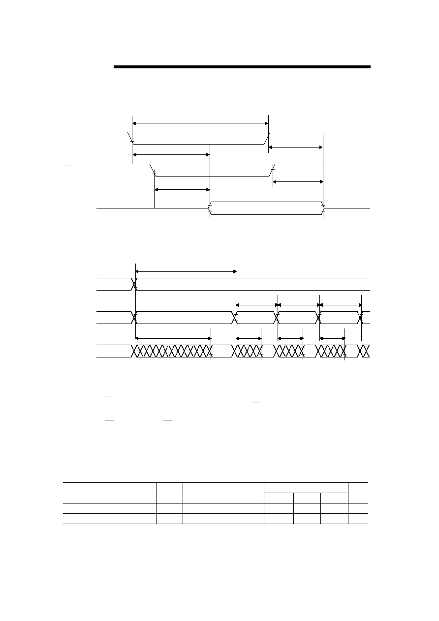
MSM538052E
6
CE
t
C
OE
D
OUT
t
CE
t
CHZ
t
OE
Page Mode Read Cycle (Note4)
Address
A3 - A17
t
PSET
D
OUT
t
ACC
t
PAC
t
PAC
t
PAC
t
PC
t
PC
t
PC
Address
A0 - A2
Read Cycle (Note2)
(Note 3)
Note)
1. CE is low level.
2. Address is fixed before or at the same time when CE level falls.
3. t
CHZ
& t
OHZ
indicate the time until floating. They are not determined by the output level.
4. CE is low level and OE is low level.
I/O CAPACITANCE
Input Capacitance
Output Capacitance
Parameter
Symbol
C
I
Unit
8
Typ.
Conditions
Min.
Max.
C
O
pF
10
Rated Value
pF
V
I
=0V
V
O
=0V
--
--
--
--
t
OHZ
(Note 3)

Page 1
Semiconductor
NOTICE
The information contained herein can change without notice owing to product and/or technical im-
provements. Before using the product, please make sure that the information being referred to is up-to-
date.
The outline of action and examples for application circuits described herein have been chosen as an
explanation for the standard action and performance of the product. When planning to use the product,
please ensure that the external conditions are reflected in the actual circuit, assembly, and program
designs.
When designing your product, please use our product below the specified maximum ratings and within
the specified operating ranges including, but not limited to, operating voltage, power dissipation, and
operating temperature.
Oki assumes no responsibility or liability whatsoever for any failure or unusual or unexpected opera-
tion resulting from misuse, neglect, improper installation, repair, alteration or accident, improper han-
dling, or unusual physical or electrical stress including, but not limited to, exposure to parameters be-
yond the specified maximum ratings or operation outside the specified operating range.
Neither indemnity against nor license of a third party's industrial and intellectual property right, etc. is
granted by us in connection with the use of the product and/or the information and drawings contained
herein. No responsibility is assumed by us for any infringement of a third party's right which may result
from the use thereof.
The products listed in this document are intended for use in general electronics equipment for commer-
cial applications (e.g., office automation, communication equipment, measurement equipment, consumer
electronics, etc.). These products are not authorized for use in any system orapplication that requires
special or enhanced quality and reliability characteristics nor in any system or application where the
failure of such system or application may result in the loss or damage of property, or death or injury to
humans. Such applications include, but are not limited to, traffic and automotive equipment, safety de-
vices, aerospace equipment, nuclear power control, medical equipment, and life-support systems.
Certain products in this document may need government approval before they can be exported to par-
ticular countries. The purchaser assumes the responsibility of determining the legality of export of these
products and will take appropriate and necessary steps at their own expense for these.
No part of the contents cotained herein may be reprinted or reproduced without our prior permission.
All brand, company and product names are the trademarks or registered trademarks of their respective
owners.
Copyright 1998 Oki Electric Industry Co., Ltd.
Marketing Communications Team (RB)

ADDRESSES & SEMICONDUCTOR WEB SITES
OKI Electric Industry Co., Ltd.
OKI Electric Industry Co., Ltd.
OKI Electric Industry Co., Ltd.
OKI Electric Industry Co., Ltd.
OKI Electric Industry Co., Ltd.,
Device Business Group,
10-3, Shibaura, 4-chome,
Minato-ku, Tokyo 108, Japan,
Tel.: +81-(0)3-5445-6327,
Fax.: +81-(0)3-5445-6328,
http://www.oki.co.jp/semi/
OKI Semiconductor Group
OKI Semiconductor Group
OKI Semiconductor Group
OKI Semiconductor Group
OKI Semiconductor Group,
785 North Mary Avenue,
Sunnyvale, CA 94086, U.S.A.,
Tel.: +1-408-720-1900,
Fax.: +1-408-720-1918,
http://www.okisemi.com/
OKI Electric Europe GmbH
OKI Electric Europe GmbH
OKI Electric Europe GmbH
OKI Electric Europe GmbH
OKI Electric Europe GmbH,
Head Office Europe,
Hellersbergstrasse 2,
D-41460 Neuss, Germany,
Tel: +49-2131-15960,
Fax: +49-2131-103539,
http://www.oki-europe.de/
OKI Electronics (Hong Kong) Ltd.
OKI Electronics (Hong Kong) Ltd.
OKI Electronics (Hong Kong) Ltd.
OKI Electronics (Hong Kong) Ltd.
OKI Electronics (Hong Kong) Ltd.,
Suite 1901-1&19, Tower 3,
China Hong Kong City,
33 Canton Road, Tsimshatsui,
Kowloon, Hong Kong,
Tel.: +852-2-736-2336,
Fax.: +852-2-736-2395
OKI Semiconductor (Asia) Pte. Ltd.
OKI Semiconductor (Asia) Pte. Ltd.
OKI Semiconductor (Asia) Pte. Ltd.
OKI Semiconductor (Asia) Pte. Ltd.
OKI Semiconductor (Asia) Pte. Ltd.,
78 Shenton Way 09-01,
Singapore 0207,
Tel.: +65-221-3722,
Fax.: +65-323-5376
OKI Semiconductor (Asia) Pte. Ltd.
OKI Semiconductor (Asia) Pte. Ltd.
OKI Semiconductor (Asia) Pte. Ltd.
OKI Semiconductor (Asia) Pte. Ltd.
OKI Semiconductor (Asia) Pte. Ltd.,
Taipei Branch,
7th Fl. No.260, Tun Hwa North Road,
Taipei, Taiwan, R.O.C.,
Sumitomo-Flysun Building,
Tel.: +886-2-2719-2561,
Fax.: +886-2-2715-2892
http://www.oki.net.tw/
For further information, please contact:
People To People Technology