
OKI Semiconductor
FEDS5412222B-01
Issue Date: Nov.,20, 2002
MSM5412222B
262,214-Word
◊ 12-Bit Field Memory
1/17
GENERAL DESCRIPTION
The OKI MSM5412222B is a high performance 3-Mbit, 256K
◊ 12-bit, Field Memory. It is especially designed
for high-speed serial access applications such as HDTVs, conventional NTSC TVs, VTRs, digital movies and
Multi-media systems. MSM5412222B is a FRAM for wide or low end use in general commodity TVs and VTRs
exclusively. MSM5412222B is not designed for the other use or high end use in medical systems, professional
graphics systems which require long term picture storage, data storage systems and others. More than two
MSM5412222Bs can be cascaded directly without any delay devices among the MSM5412222Bs. (Cascading of
MSM5412222B provides larger storage depth or a longer delay).
Each of the 12-bit planes has separate serial write and read ports. These employ independent control clocks to
support asynchronous read and write operations. Different clock rates are also supported that allow alternate data
rates between write and read data streams.
The MSM5412222B provides high speed FIFO, First-In First-Out, operation without external refreshing:
MSM5412222B refreshes its DRAM storage cells automatically, so that it appears fully static to the users.
Moreover, fully static type memory cells and decoders for serial access enable the refresh free serial access
operation, so that serial read and/or write control clock can be halted high or low for any duration as long as the
power is on. Internal conflicts of memory access and refreshing operations are prevented by special arbitration
logic.
The MSM5412222B's function is simple, and similar to a digital delay device whose delay-bit-length is easily set
by reset timing. The delay length, number of read delay clocks between write and read, is determined by externally
controlled write and read reset timings.
Additional SRAM serial registers, or line buffers for the initial access of 256
◊ 12-bit enable high speed
first-bit-access with no clock delay just after the write or read reset timings.
Additionally, the MSM5412222B has write mask function or input enable function (IE), and read-data skipping
function or output enable function (OE) . The differences between write enable (WE) and input enable (IE), and
between read enable (RE) and output enable (OE) are that WE and RE can stop serial write/read address
increments, but IE and OE cannot stop the increment, when write/read clocking is continuously applied to
MSM5412222B. The input enable (IE) function allows the user to write into selected locations of the memory
only, leaving the rest of the memory contents unchanged. This facilitates data processing to display a "picture in
picture" on a TV screen.
The MSM5412222B is similar in operation and functionality to OKI 1-Mbit Field Memory MSM514222C and
2-Mbit Field Memory MSM518222A. Three MSM514222Cs or one MSM514222C plus one MSM518222A can
be replaced simply by one MSM5412222B.
FEDS5412222B-01
OKI Semiconductor
MSM5412222B
2/17
FEATURES
∑ Single power supply: 5.0 V ±0.5 V
∑ 262,214
words
◊ 12 bits
∑ Fast FIFO (First-In First-Out) operation
∑ High speed asynchronous serial access
Read/write cycle time 25 ns/30 ns
Access time
23 ns/25 ns
∑ Direct cascading capability
∑ Write mask function (Input enable control)
∑ Data skipping function (Output enable control)
∑ Self refresh (No refresh control is required)
∑ Package
options:
44-pin 400 mil plastic TSOP (Type 2)
(TSOP(2)44-P-400-0.80-K) (Product:MSM5412222B-xxTS-K)
40-pin 400 mil plastic SOJ
(SOJ40-P-400-1.27)
(Product: MSM5412222B-xxJS)
xx indicates speed rank.
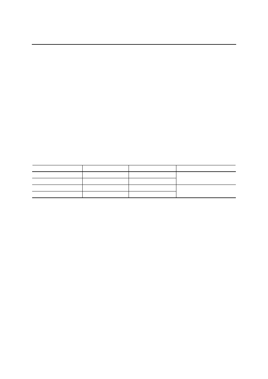
PRODUCT FAMILY
Family
Access Time (Max.)
Cycle Time (Min.)
Package
MSM5412222B-25TS-K
23 ns
25 ns
MSM5412222B-30TS-K
25 ns
30 ns
400 mil 44-pin TSOP (2)
MSM5412222B-25JS
23 ns
25 ns
MSM5412222B-30JS
25 ns
30 ns
400 mil 40-pin SOJ

FEDS5412222B-01
OKI Semiconductor
MSM5412222B
3/17
PIN CONFIGURATION (TOP VIEW)
Pin Name
Function
SWCK
Serial Write Clock
SRCK
Serial Read Clock
WE Write
Enable
RE Read
Enable
IE Input
Enable
OE Output
Enable
RSTW
Write Reset Clock
RSTR
Read Reset Clock
D
IN
0 to 11
Data Input
D
OUT
0 to 11
Data Output
V
CC
Power Supply (5.0 V)
V
SS
Ground (0 V)
NC No
Connection
Note: The same power supply voltage must be provided to every V
CC
pin, and the same GND voltage
level must be provided to every V
SS
pin.
V
SS
V
CC
D
OUT
11
D
OUT
10
D
OUT
9
D
OUT
8
D
OUT
7
D
OUT
6
D
OUT
5
D
OUT
4
D
OUT
3
D
OUT
2
D
OUT
1
D
OUT
0
SRCK
RSTR
RE
OE
V
SS
V
CC
40
39
38
37
36
35
34
33
32
31
30
29
28
27
26
25
24
23
22
21
1
2
3
4
5
6
7
8
9
10
11
12
13
14
15
16
17
18
19
20
V
SS
NC
D
IN
11
D
IN
10
D
IN
9
D
IN
8
D
IN
7
D
IN
6
D
IN
5
D
IN
4
D
IN
3
D
IN
2
D
IN
1
D
IN
0
SWCK
RSTW
WE
IE
NC
V
CC
V
SS
D
OUT
11
D
OUT
10
NC
D
OUT
9
D
OUT
8
D
OUT
7
D
OUT
6
V
CC
D
OUT
5
D
OUT
4
D
OUT
3
D
OUT
2
V
SS
D
OUT
1
D
OUT
0
SRCK
RSTR
NC
RE
OE
V
CC
1
2
3
4
5
6
7
8
9
10
11
12
13
14
15
16
17
18
19
20
21
22
44
43
42
41
40
39
38
37
36
35
34
33
32
31
30
29
28
27
26
25
24
23
V
SS
D
IN
11
D
IN
10
NC
D
IN
9
D
IN
8
D
IN
7
D
IN
6
NC
D
IN
5
D
IN
4
D
IN
3
D
IN
2
NC
D
IN
1
D
IN
0
SWCK
RSTW
NC
WE
IE
V
CC
44-Pin Plastic TSOP (2)
(K Type)
40-Pin Plastic SOJ
FEDS5412222B-01
OKI Semiconductor
MSM5412222B
4/17
BLOCK DIAGRAM
Clock
Oscillator
X
262,144
◊
12
Memory
Array
Serial Read Re
g
ister
(
◊
12
)
Read Line Buffer
W
r
ite Line Buffer
(
◊
12
)
Serial Read Controller
RE
RST
R
SRCK
Data-Out
Buffer (
◊
12)
D
OUT
(
◊
12)
Read/W
r
ite
and Refresh
Controller
Sub-Register (
◊
12)
Decoder
OE
(
◊
12)
71-W
o
rd
Sub-Register (
◊
12)
Serial W
r
ite Register (
◊
12)
71-W
o
rd
V
BB
Generator
WE
RST
W
SWCK
Data-In
Buffer (
◊
12)
D
IN
(
◊
12)
IE
Serial W
r
ite Controller

FEDS5412222B-01
OKI Semiconductor
MSM5412222B
5/17
OPERATION
Write Operation
The write operation is controlled by three clocks, SWCK, RSTW, and WE. Write operation is accomplished by
cycling SWCK, and holding WE high after the write address pointer reset operation or RSTW.
Each write operation, which begins after RSTW, must contain at least 150 active write cycles, i.e. SWCK cycles
while WE is high. To transfer the last data to the DRAM array, which at that time is stored in the serial data
registers attached to the DRAM array, an RSTW operation is required after the last SWCK cycle.
Note that every write timing of MSM5412222B is delayed by one clock compared with read timings for easy
cascading without any interface delay devices.
Write Reset: RSTW
The first positive transition of SWCK after RSTW becomes high resets the write address counters to zero. RSTW
setup and hold times are referenced to the rising edge of SWCK. Because the write reset function is solely
controlled by the SWCK rising edge after the high level of RSTW, the states of WE and IE are ignored in the write
reset cycle.
Before RSTW may be brought high again for a further reset operation, it must be low for at least two SWCK
cycles.
Data Inputs: D
IN
0 to 11
Write Clock: SWCK
The SWCK latches the input data on chip when WE is high, and also increments the internal write address pointer.
Data-in setup time t
DS
, and hold time t
DH
are referenced to the rising edge of SWCK.
Write Enable: WE
WE is used for data write enable/disable control. WE high level enables the input, and WE low level disables the
input and holds the internal write address pointer. There are no WE disable time (low) and WE enable time (high)
restrictions, because the MSM5412222B is in fully static operation as long as the power is on. Note that WE setup
and hold times are referenced to the rising edge of SWCK.
Input Enable: IE
IE is used to enable/disable writing into memory. IE high level enables writing. The internal write address pointer
is always incremented by cycling SWCK regardless of the IE level. Note that IE setup and hold times are
referenced to the rising edge of SWCK.

FEDS5412222B-01
OKI Semiconductor
MSM5412222B
6/17
Read Operation
The read operation is controlled by three clocks, SRCK, RSTR, and RE. Read operation is accomplished by
cycling SRCK, and holding RE high after the read address pointer reset operation or RSTR.
Each read operation, which begins after RSTR, must contain at least 150 active read cycles, i.e. SRCK cycles while
RE is high.
Read Reset: RSTR
The first positive transition of SRCK after RSTR becomes high resets the read address counters to zero. RSTR
setup and hold times are referenced to the rising edge of SRCK. Because the read reset function is solely controlled
by the SRCK rising edge after the high level of RSTR, the states of RE and OE are ignored in the read reset cycle.
Before RSTR may be brought high again for a further reset operation, it must be low for at least *two SRCK
cycles.
Data Out: D
OUT
0 to 11
Read Clock: SRCK
Data is shifted out of the data registers. It is triggered by the rising edge of SRCK when RE is high during a read
operation. The SRCK input increments the internal read address pointer when RE is high.
The three-state output buffer provides direct TTL compatibility (no pullup resistor required). Data out is the same
polarity as data in. The output becomes valid after the access time interval t
AC
that begins with the rising edge of
SRCK. *There are no output valid time restriction on MSM5412222B.
Read Enable: RE
The function of RE is to gate of the SRCK clock for incrementing the read pointer. When RE is high before the
rising edge of SRCK, the read pointer is incremented. When RE is low, the read pointer is not incremented. RE
setup times (t
RENS
and t
RDSS
) and RE hold times (t
RENH
and t
RDSH
) are referenced to the rising edge of the SRCK
clock.
Output Enable: OE
OE is used to enable/disable the outputs. OE high level enables the outputs. The internal read address pointer is
always incremented by cycling SRCK regardless of the OE level. Note that OE setup and hold times are referenced
to the rising edge of SRCK.

FEDS5412222B-01
OKI Semiconductor
MSM5412222B
7/17
Power-up and Initialization
On power-up, the device is designed to begin proper operation after at least 100
µs after V
CC
has stabilized to a
value within the range of recommended operating conditions. After this 100
µs stabilization interval, the following
initialization sequence must be performed.
Because the read and write address counters are not valid after power-up, a minimum of 80 dummy write
operations (SWCK cycles) and read operations (SRCK cycles) must be performed, followed by an RSTW
operation and an RSTR operation, to properly initialize the write and the read address pointer. Dummy write
cycles/RSTW and dummy read cycles/RSTR may occur simultaneously.
If these dummy read and write operations start while V
CC
and/or the substrate voltage has not stabilized, it is
necessary to perform an RSTR operation plus a minimum of 80 SRCK cycles plus another RSTR operation, and an
RSTW operation plus a minimum of 80 SRCK cycles plus another RSTW operation to properly initialize read and
write address pointers.
Old/New Data Access
There must be a minimum delay of 150 SWCK cycles between writing into memory and reading out from memory.
If reading from the first field starts with an RSTR operation, before the start of writing the second field (before the
next RSTW operation), then the data just written will be read out.
The start of reading out the first field of data may be delayed past the beginning of writing in the second field of
data for as many as 20 SWCK cycles. If the RSTR operation for the first field read-out occurs less than 20 SWCK
cycles after the RSTW operation for the second field write-in, then the internal buffering of the device assures that
the first field will still be read out. The first field of data that is read out while the second field of data is written is
called "old data".
In order to read out "new data", i.e., the second field written in, the delay between an RSTW operation and an
RSTR operation must be at least 150 SRCK cycles. If the delay between RSTW and RSTR operations is more than
21 but less than 150 cycles, then the data read out will be undetermined. It may be "old data" or "new" data, or a
combination of old and new data. Such a timing should be avoided.
Cascade Operation
The MSM5412222B is designed to allow easy cascading of multiple memory devices. This provides higher
storage depth, or a longer delay than can be achieved with only one memory device.
FEDS5412222B-01
OKI Semiconductor
MSM5412222B
8/17
ELECTRICAL CHARACTERISTICS
Absolute Maximum Ratings
Parameter Symbol
Conditon
Rating Unit
Input Output Voltage
V
T
at Ta = 25
∞
C, V
SS
≠1.0 to +7.0
V
Output Current
I
OS
Ta = 25
∞
C 50
mA
Power Dissipation
P
D
Ta = 25
∞
C 1
W
Operating Temperature
T
opr
--
0 to 70
∞
C
Storage Temperature
T
stg
--
≠55 to +150
∞
C
Recommended Operating Conditions
Parameter Symbol
Min.
Typ
Max. Unit
Power Supply Voltage
V
CC
4.5
5.0
5.5
V
Input High Voltage
V
IH
2.4
V
CC
V
CC
+1
V
Input Low Voltage
V
IL
≠0.1
0
+0.8 V
DC Characteristics
Parameter Symbol
Condition
Min.
Max.
Unit
Input Leakage Current
I
LI
0 < V
I
< V
CC
+ 1 V, Other Pins Tested at V = 0 V
≠10
+10
µA
Output Leakage Current
I
LO
0 < V
O
< V
CC
≠10
+10
µA
Output "H" Level Voltage
V
OH
I
OH
= ≠1 mA
2.4
--
V
Output "L" Level Voltage
V
OL
I
OL
= 2 mA
--
0.4
V
Operating Current
I
CC1
Minimum Cycle Time, Output Open
--
60
mA
Standby Current
I
CC2
Input Pin = V
IH
/V
IL
--
5
mA
Capacitance
(Ta = 25∞C, f = 1 MHz)
Parameter Symbol
Max.
Unit
Input Capacitance (D
IN
,
SWCK, SRCK, RSTW, RSTR, WE, RE, IE, OE)
C
I
6 pF
Output Capacitance (D
OUT
) C
O
7 pF

FEDS5412222B-01
OKI Semiconductor
MSM5412222B
9/17
AC Characteristics
(V
CC
= 5.0 V ±0.5 V, Ta = 0 to 70∞C)
MSM5412222B-25 MSM5412222B-30
Parameter Symbol
Min. Max. Min. Max.
Unit
Access Time from SRCK
t
AC
-- 23 -- 25 ns
D
OUT
Hold Time from SRCK
t
DDCK
6 -- 6 -- ns
D
OUT
Enable Time from SRCK
t
DECK
6 23 6 25 ns
SWCK "H" Pulse Width
t
WSWH
9 -- 12 -- ns
SWCK "L" Pulse Width
t
WSWL
10 -- 12 -- ns
Input Data Setup Time
t
DS
2 -- 2 -- ns
Input Data Hold Time
t
DH
4 -- 4 -- ns
WE Enable Setup Time
t
WENS
0 -- 0 -- ns
WE Enable Hold Time
t
WENH
3 -- 3 -- ns
WE Disable Setup Time
t
WDSS
0 -- 0 -- ns
WE Disable Hold Time
t
WDSH
3 -- 3 -- ns
IE Enable Setup Time
t
IENS
0 -- 0 -- ns
IE Enable Hold Time
t
IENH
3 -- 3 -- ns
IE Disable Setup Time
t
IDSS
0 -- 0 -- ns
IE Disable Hold Time
t
IDSH
3 -- 3 -- ns
WE "H" Pulse Width
t
WWEH
5 -- 10 -- ns
WE "L" Pulse Width
t
WWEL
5 -- 10 -- ns
IE "H" Pulse Width
t
WIEH
5 -- 10 -- ns
IE "L" Pulse Width
t
WIEL
5 -- 10 -- ns
RSTW Setup Time
t
RSTWS
0 -- 0 -- ns
RSTW Hold Time
t
RSTWH
3 -- 3 -- ns
SRCK "H" Pulse Width
t
WSRH
9 -- 12 -- ns
SRCK "L" Pulse Width
t
WSRL
10 -- 12 -- ns
RE Enable Setup Time
t
RENS
0 -- 0 -- ns
RE Enable Hold Time
t
RENH
3 -- 3 -- ns
RE Disable SetupTime
t
RDSS
0 -- 0 -- ns
RE Disable Hold Time
t
RDSH
3 -- 3 -- ns
OE Enable Setup Time
t
OENS
0 -- 0 -- ns
OE Enable Hold Time
t
OENH
3 -- 3 -- ns
OE Disable SetupTime
t
ODSS
0 -- 0 -- ns
OE Disable Hold Time
t
ODSH
3 -- 3 -- ns
Output Buffer Turn-off Delay Time from OE
t
OEZ
17 -- 17 -- ns
RE "H" Pulse Width
t
WREH
5 -- 10 -- ns
RE "L" Pulse Width
t
WREL
5 -- 10 -- ns
OE "H" Pulse Width
t
WOEH
5 -- 10 -- ns
OE "L" Pulse Width
t
WOEL
5 -- 10 -- ns
RSTR Setup Time
t
RSTRS
0 -- 0 -- ns
RSTR Hold Time
t
RSTRH
3 -- 3 -- ns
SWCK Cycle Time
t
SWC
25 -- 30 -- ns
SRCK Cycle Time
t
SRC
25 -- 30 -- ns
Transition Time (Rise and Fall)
t
T
3 30 3 30 ns

FEDS5412222B-01
OKI Semiconductor
MSM5412222B
10/17
Notes: 1. Input signal reference levels for the parameter measurement are V
IH
= 3.0 V and V
IL
= 0 V. The
transition time t
T
is defined to be a transition time that signal transfers between V
IH
= 3.0 V and
V
IL
= 0 V.
2. AC measurements assume t
T
= 3 ns.
3. Read address must have more than a 150 address delay than write address in every cycle
when asynchronous read/write is performed.
4. Read must have more than a 150 address delay than write in order to read the data written in
a current series of write cycles which has been started at last write reset cycle: this is called
"new data read".
When read has less than a 20 address delay than write, the read data are the data written in a
previous series of write cycles which had been written before at last write reset cycle: this is
called "old data read".
5. When the read address delay is between more than 21 and less than 149, read data will be
undetermined. However, normal write is achieved in this address condition.
6. Outputs are measured with a load equivalent to 1 TTL load and 30 pF.
Output reference levels are V
OH
= 2.0 V and V
OL
= 0.8 V.
FEDS5412222B-01
OKI Semiconductor
MSM5412222B
11/17
TIMING WAVEFORM
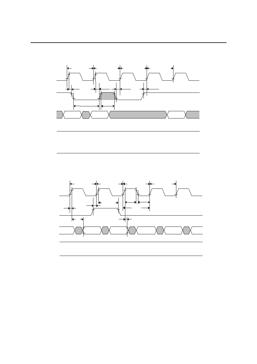
Write Cycle Timing (Write Reset)
SWCK
RSTW
D
IN
WE
n ≠ 1
n
0
1
2
n cycle
0 cycle
1 cycle
2 cycle
t
T
t
RSTWS
t
RSTWH
t
SWC
t
DS
t
DH
t
WSWH
t
WSWL
≠V
IH
≠V
IL
≠V
IH
≠V
IL
≠V
IH
≠V
IL
≠V
IH
≠V
IL
IE
≠V
IH
≠V
IL
Write Cycle Timing (Write Enable)
SWCK
WE
IE
n ≠ 1
n cycle
Disable cycle
Disable cycle
n + 1 cycle
t
WENH
t
WDSS
t
WENS
t
WWEL
t
WWEH
t
WDSH
n + 1
≠V
IH
≠V
IL
≠V
IH
≠V
IL
≠V
IH
≠V
IL
≠V
IH
≠V
IL
D
IN
n
RSTW
≠V
IH
≠V
IL
FEDS5412222B-01
OKI Semiconductor
MSM5412222B
12/17
Write Cycle Timing (Input Enable)
SWCK
IE
D
IN
WE
n ≠ 1
n + 3
n cycle
n + 1 cycle
n + 2 cycle
n + 3 cycle
t
IENH
t
IDSS
t
IENS
t
WIEL
t
WIEH
t
IDSH
n
RSTW
≠V
IH
≠V
IL
≠V
IH
≠V
IL
≠V
IH
≠V
IL
≠V
IH
≠V
IL
≠V
IH
≠V
IL
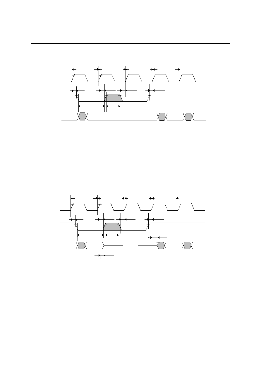
Read Cycle Timing (Read Reset)
SRCK
RSTR
D
OUT
RE
n ≠ 1
n
0
1
2
n cycle
0 cycle
1 cycle
2 cycle
t
T
t
RSTRS
t
RSTRH
t
SRC
t
AC
t
WSRH
t
WSRL
OE
t
DDCK
≠V
IH
≠V
IL
≠V
IH
≠V
IL
≠V
IH
≠V
IL
≠V
IH
≠V
IL
≠V
OH
≠V
OL
FEDS5412222B-01
OKI Semiconductor
MSM5412222B
13/17
Read Cycle Timing (Read Enable)
SRCK
RE
OE
n + 1
n cycle
Disable cycle
Disable cycle
n + 1 cycle
n
RSTR
≠V
IH
≠V
IL
≠V
IH
≠V
IL
≠V
IH
≠V
IL
≠V
OH
≠V
OL
≠V
IH
≠V
IL
t
RENH
t
WREL
t
RDSH
t
RDSS
t
WREH
t
RENS
D
OUT
n ≠ 1
Read Cycle Timing (Output Enable)
SRCK
OE
D
OUT
RSTR
n ≠ 1
n + 3
≠V
IH
n cycle
n + 1 cycle
n + 2 cycle
n + 3 cycle
t
OENH
t
WOEL
t
ODSH
t
ODSS
t
WOEH
n
Hi-Z
t
DECK
t
OENS
≠V
IL
≠V
IH
≠V
IL
≠V
IH
≠V
IL
≠V
OH
≠V
OL
RE
≠V
IH
≠V
IL
t
OEZ
FEDS5412222B-01
OKI Semiconductor
MSM5412222B
14/17
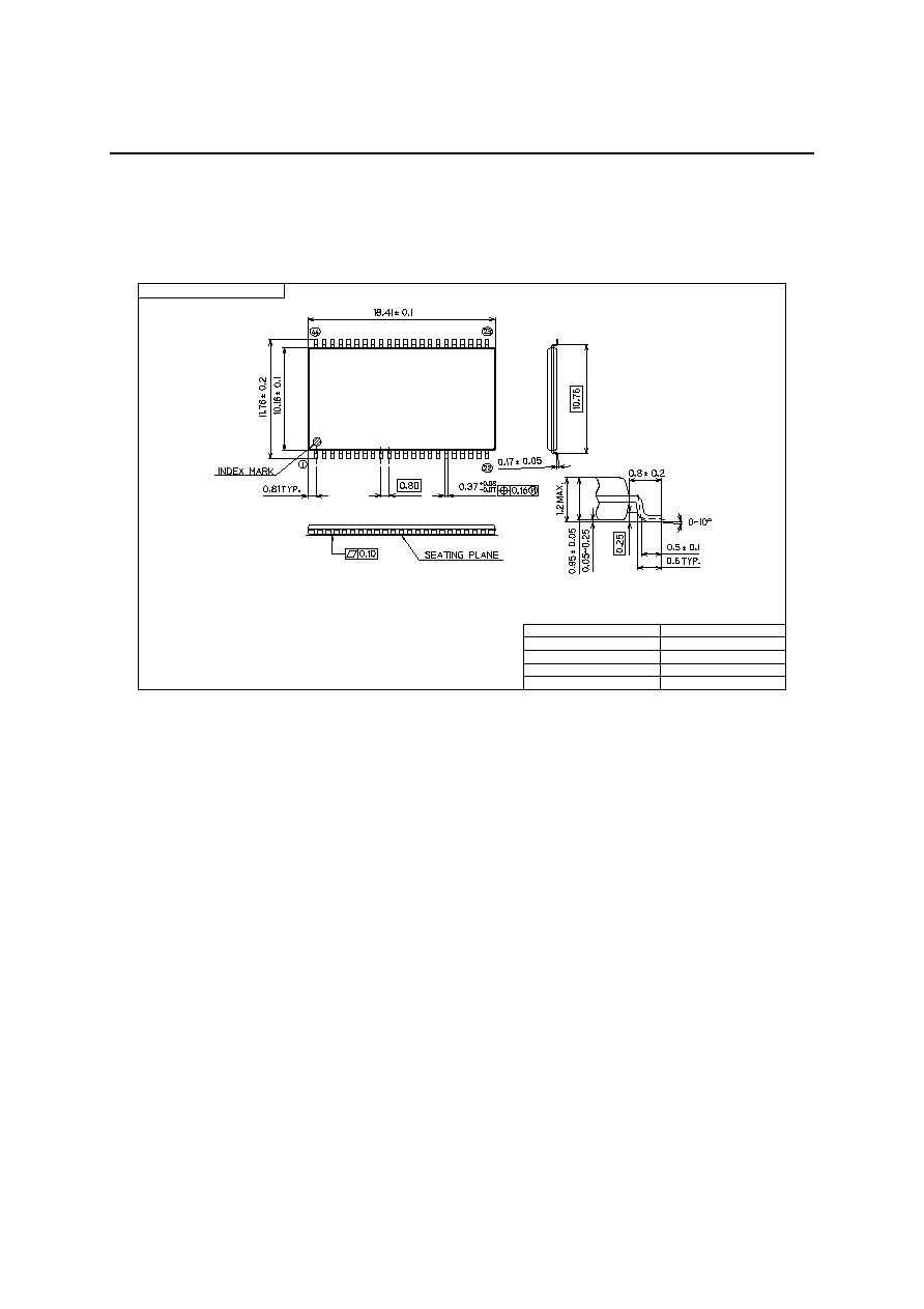
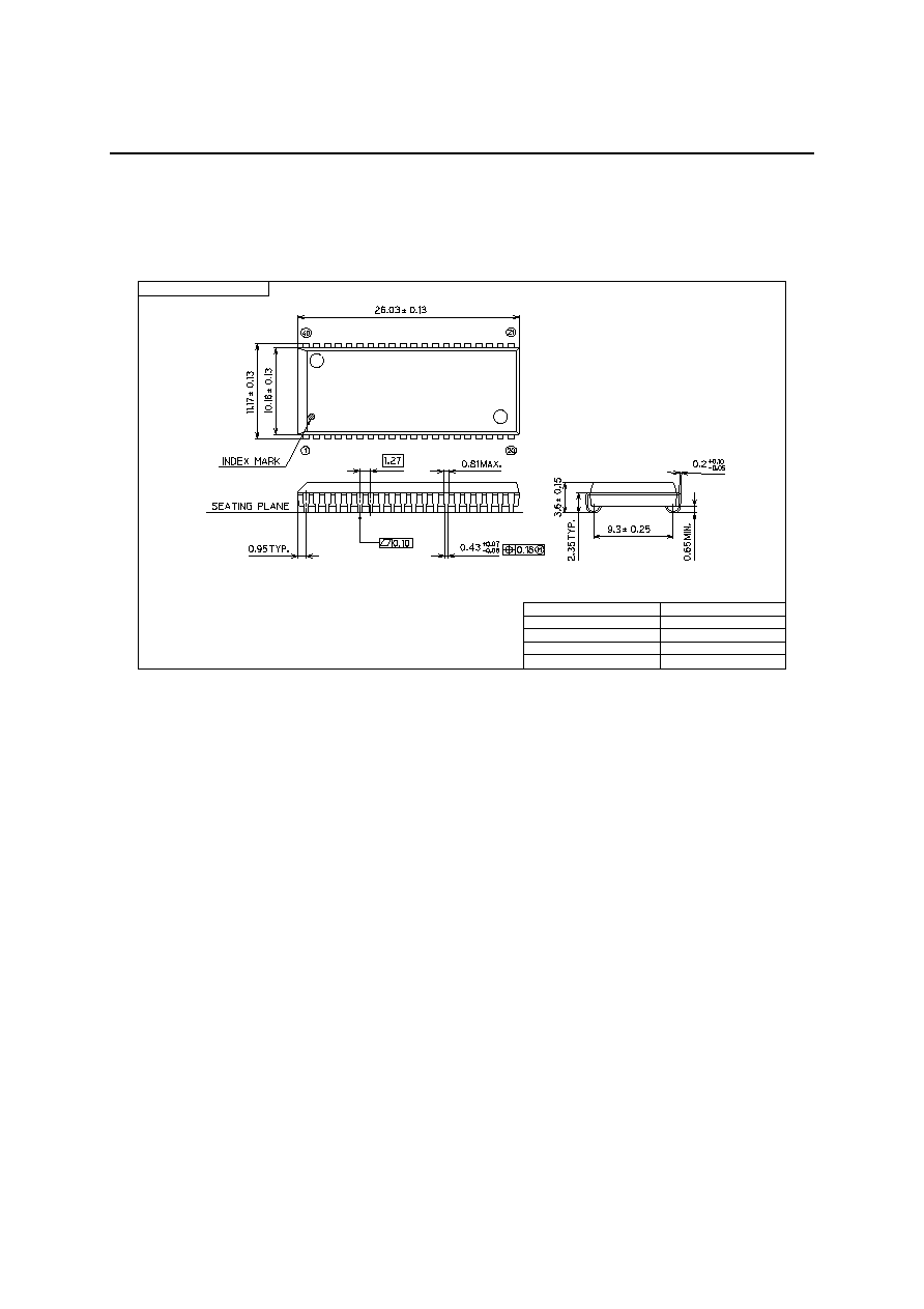
PACKAGE DIMENSIONS
Notes for Mounting the Surface Mount Type Packages
The surface mount type packages are very susceptible to heat in reflow mounting and humidity
absorbed in storage.
Therefore, before you perform reflow mounting, contact Oki's responsible sales person for the product
name, package name, pin number, package code and desired mounting conditions (reflow method,
temperature and times).
TSOP(2)44-P-400-0.80-K
Mirror finish
Package material
Epoxy resin
Lead frame material
42 alloy
Pin treatment
Solder plating (
5µm)
Package weight (g)
0.54 TYP.
5
Rev. No./Last Revised
3/Dec. 10, 1996
(Unit: mm)
FEDS5412222B-01
OKI Semiconductor
MSM5412222B
15/17
Notes for Mounting the Surface Mount Type Packages
The surface mount type packages are very susceptible to heat in reflow mounting and humidity
absorbed in storage.
Therefore, before you perform reflow mounting, contact Oki's responsible sales person for the product
name, package name, pin number, package code and desired mounting conditions (reflow method,
temperature and times).
SOJ40-P-400-1.27
Mirror finish
Package material
Epoxy resin
Lead frame material
42 alloy
Pin treatment
Solder plating (
5µm)
Package weight (g)
1.70 TYP.
5
Rev. No./Last Revised
5/Dec. 5, 1996
(Unit: mm)

FEDS5412222B-01
OKI Semiconductor
MSM5412222B
16/17
REVISION HISTORY
Page
Document
No.
Date
Previous
Edition
Current
Edition
Description
FEDS5412222B-01
Nov.,20 , 2002
≠
≠
Final edition 1

FEDS5412222B-01
OKI Semiconductor
MSM5412222B
17/17
NOTICE
1. The information contained herein can change without notice owing to product and/or technical improvements.
Before using the product, please make sure that the information being referred to is up-to-date.
2. The outline of action and examples for application circuits described herein have been chosen as an
explanation for the standard action and performance of the product. When planning to use the product, please
ensure that the external conditions are reflected in the actual circuit, assembly, and program designs.
3. When designing your product, please use our product below the specified maximum ratings and within the
specified operating ranges including, but not limited to, operating voltage, power dissipation, and operating
temperature.
4. Oki assumes no responsibility or liability whatsoever for any failure or unusual or unexpected operation
resulting from misuse, neglect, improper installation, repair, alteration or accident, improper handling, or
unusual physical or electrical stress including, but not limited to, exposure to parameters beyond the specified
maximum ratings or operation outside the specified operating range.
5. Neither indemnity against nor license of a third party's industrial and intellectual property right, etc. is
granted by us in connection with the use of the product and/or the information and drawings contained herein.
No responsibility is assumed by us for any infringement of a third party's right which may result from the use
thereof.
6. The products listed in this document are intended for use in general electronics equipment for commercial
applications (e.g., office automation, communication equipment, measurement equipment, consumer
electronics, etc.). These products are not authorized for use in any system or application that requires special
or enhanced quality and reliability characteristics nor in any system or application where the failure of such
system or application may result in the loss or damage of property, or death or injury to humans.
Such applications include, but are not limited to, traffic and automotive equipment, safety devices, aerospace
equipment, nuclear power control, medical equipment, and life-support systems.
7. Certain products in this document may need government approval before they can be exported to particular
countries. The purchaser assumes the responsibility of determining the legality of export of these products
and will take appropriate and necessary steps at their own expense for these.
8.
No part of the contents contained herein may be reprinted or reproduced without our prior permission.
Copyright 2002 Oki Electric Industry Co., Ltd.