FEATURES
∑ 262,144-word by 16-bit configuration
∑ Single 5V power supply,
±
10% tolerance
∑ Input :TTL compatible
∑ Output :TTL compatible, 3-state
∑ Refresh : 512 cycles/8ms
∑ Fast page mode with EDO,read modify write capability
∑ Byte wide control: 2 CAS control
∑ CAS before RAS refresh, Hidden refresh, RAS only refresh capability
∑ Package : 40-Pin 400 mil plastic SOJ (SOJ40-P-400)
(Product : MSM5416258B-xxJS) xx : indicates speed rank.
DESCRIPTION
OKI Semiconductor
MSM5416258B
262,144-Word x 16-Bit DYNAMIC RAM : FAST PAGE MODE TYPE WITH EDO
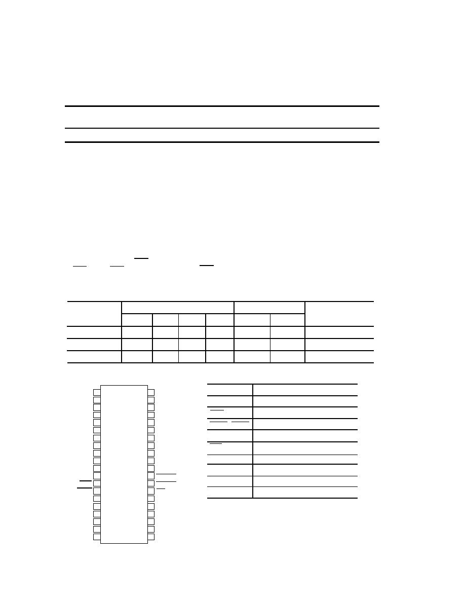
PIN CONFIGURATION ( TOP VIEW )
The MSM5416258B is a 262,144-word x 16-bit dynamic RAM fabricated in OKI's CMOS silicon gate
technology. The MSM5416258B achieves high integration,high-speed operation,and low-power
consumption due to quadruple polysilicon double metal CMOS. The MSM5416258B is available in a
40-pin plastic SOJ.
PRODUCT FAMILY
Family
Access Time (Max.)
Cycle Time (Min.)
Power Dissipation
t
RAC
t
AA
t
RC
t
HPC
MSM5416258B-30
30ns 16ns
55ns 13ns
1458mW
REVISION-2 1997.11.10, specification are subject to change without advanced notice.
1/20
Vcc
DQ0
DQ1
DQ2
DQ3
Vcc
DQ4
DQ5
DQ6
DQ7
NC
NC
WE
RAS
NC
A0
A1
A2
A3
Vcc
Vss
DQ15
DQ14
DQ13
DQ12
Vss
DQ11
DQ10
DQ9
DQ8
NC
LCAS
UCAS
OE
A8
A7
A6
A5
A4
Vss
1
2
3
4
5
6
7
8
9
10
11
12
13
14
15
16
17
18
19
20
40
39
38
37
36
35
34
33
32
31
30
29
28
27
26
25
24
23
22
21
40Pin 400mil SOJ
OE
Row Address Strobe
Data-Input/ Data-Output
DQ0-15
LCAS,UCAS
WE
Column Address Strobe
Output Enable
Pin Names
Function
A0-A8
RAS
Vcc
Vss
NC
Address Input
Write Enable
Power Supply ( +5V )
Ground ( 0V )
No Connection
t
CAC
9ns
t
OEA
9ns
Note1 : The same power supply voltage must be
provided to every Vcc pin, and the same
GND voltage level must beprovideded to
every Vss pin.
MSM5416258B-35
35ns 19ns
60ns 13ns
1430mW
10ns 10ns
MSM5416258B-28
Technical Information
28ns
1485mW
15ns 48ns
12ns
9ns
9ns
Input Pin
RAS LCAS
WE OE
H
*
L
L
L
L
L
L
H
L
L
L
L
L
H
L
H
H
L
L
H
L
*
H
*
*
*
*
DQPin
DQ0~DQ7 DQ8~DQ15
High-Z
High-Z High-Z
High-Z
D
OUT
D
IN
D
IN
Don
`
t Care
High-Z High-Z
Functinal Mode
Standby
Refresh
Word Read
Word Write
D
IN
Don
`
t Care
Lower Byte Write
Upper Byte Write
H
H
L
L
H
H
FUNCTION TABLE
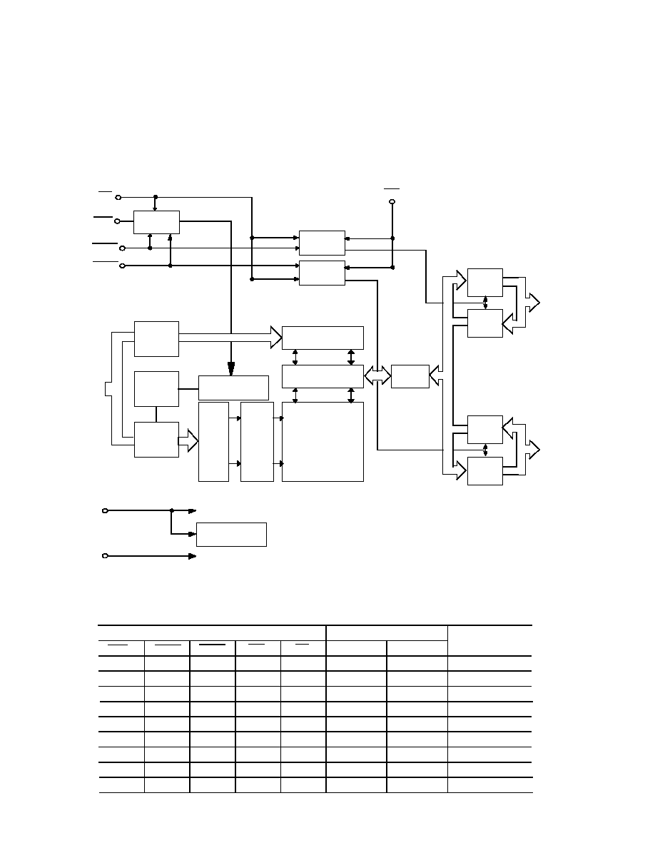
BLOCK DIAGRAM
Timing
Generater
Column
Address
Buffer
Internal
Address
Counter
Row
Address
Buffer
Refresh
Control Clock
Row
Deco-
ders
Word
Drivers
Memory
cells
Sence amplifier
Column Decoders
I/O
Controller
I/O
Controller
I/O
Selector
Output
Buffers
Input
Buffers
Input
Buffers
Output
Buffers
9
9
9
9
16
8
8
8
8
8
8
On Chip
V
BB
Generater
OE
RAS
UCAS
A0~A8
Vcc
Vss
DQ0~DQ7
DQ8~DQ15
8
8
16
WE
LCAS
UCAS
L
L
L
L
L
L
L
H
H
H
H
High-Z
D
IN
D
OUT
High-Z
D
OUT
D
OUT
Lower Byte Read
Upper Byte Read
-
Rating
Voltage on any pin relative to Vss
Short circuit output current
Power dissipation
Operrating temperrature
Storage temperature
Conditions
Ta=25
∞
C
-1.0 ~ +7.0
1.5
50
0 ~ +70
-55 ~ +150
Unit
mA
W
∞
C
V
Symbol
Vt
Ios
P
D
Topr
Tstg
Ta=25
∞
C
Ta=25
∞
C
Value
∞
C
Parameter
Supply voltage
Input high voltage
Input low voltage
Conditions
4.5
2.4
0
-1.0
Unit
V
Symbol
Vcc
Min.
Vss
V
IH
V
IL
Typ. Max.
5.0
0
5.5
6.5
0
0.8
V
V
V
Parameter
Input capacitance (A0~A8)
Input capacitance (RAS,LCAS,UCAS,WE,OE)
Input / output capacitance (DQ0~DQ15)
Conditions
Unit
pf
Symbol
C
I/0
C
IN2
Typ. Max.
8
9
8
C
IN1
pf
pf
ELECTRICAL CHARACTERISTICS
Absolute Maximum Ratings
Recommended Operating Conditions
Capacitance
(Ta=0
∞
Cto 70
∞
C)
(Vcc=5V
±
10%,Ta=25
∞
C,f=1MHz)
DC CHARACTERISTICS
- 4/20 -
Parameter
Symbol Condition
Output High Voltage
Output Low Voltage
Input Leakage Current
Output Leakage Current
0V
V
IN
Vcc
DQi Disable
0V
V
o
5.5V
RAS,CAS Cycling
t
RC
=Min.
Average Power
Supply Current
(Operating)
Power Supply
Current (Standby)
RAS,CAS = V
IH
RAS=Cycling
CAS=V
IH
t
RC
=Min.
Average Power
Supply Current
(RAS only Refresh)
Average Power
Supply Current
(CAS Before RAS
Refresh)
RAS=Cycling
CAS Befor RAS
Average Power
Supply Current
(Fast Page Mode)
RAS=V
IL
CASCycling
t
HPC=
Min.
I
OH
= - 1.0mA
I
OL
= 2.0mA
V
OH
V
OL
I
LI
I
LO
I
CC1
I
CC2
I
CC3
I
CC5
I
CC4
Note
MSM5416258B
-35
Min. Max.
MSM5416258B
-30
Min. Max.
2.4 V
cc
0
0.4
-10 10
10
-10
265
-
-
3
265
-
-
265
-
2.4 V
cc
0
0.4
-10 10
10
-10
260
-
-
3
260
-
-
260
-
Unit
V
V
µ
A
µ
A
mA
mA
mA
mA
mA
1,2
(V
cc=
5V
±
10%, Ta=0 to 70
∞
C)
1
1,2
1,3
1,2
Notes : 1. Icc Max. is specified as Icc for the output open cindition.
2. Address can be changed once or less while RAS = VIL.
3. Address can be changed once or less while CAS = VIH.
MSM5416258B
-28
Min. Max.
2.4
V
cc
0
0.4
-10
10
10
-10
-
-
3
-
-
-
270
270
270
265
260
270
Parameter
Random read or write cycle time
Read/Write cycle time
Access time from column address
Access time from OE
MIN
Symbol
t
RC
MAX
(Vcc =5V
±
10%, Ta =0~70
∞
C)
MSM5416258B
-30
Access time from RAS
Hyper page mode cycle time
Fast page mode read/write cycle time
Access time from CAS
Access time from CAS precharge
Output buffer turn-off delay time
OE to data output buffer turn-off
delay time
Transition time
Refresh preiod
RAS precharge time
RAS pulse width
RAS pulse width (Fast page mode)
RAS hold time
RAS hold time reference to OE
CAS precharge time
CAS pulse width
CAS hold time
CAS to RAS precharge time
RAS to CAS delay time
RAS to column address delay time
Row address set-up time
Row address hold time
Column address set-up time
Column address hold time
Column address hold time from RAS
Column address to RAS lead time
Read command set-up time
Read command hold time
Read command hold time
reference to RAS
t
RMW
t
HPC
t
PRMW
t
RAC
t
CAC
t
AA
t
OEA
t
CPA
t
OFF
t
OEZ
t
T
t
REF
t
RP
t
RAS
t
RASP
t
RSH
t
ROH
t
CP
t
CAS
t
CSH
t
CRP
t
RCD
t
RAD
t
ASR
t
RAH
t
ASC
t
CAH
t
AR
t
RAL
t
RCS
t
RCH
t
RRH
t
COH
Data hold after CAS low
AC CHARACTERISTICS
(1/2)
RAS to data output buffer turn-off
delay time
WE to data output buffer turn-off
delay time
t
REZ
t
WEZ
WE pulse width
t
WEP
Unit
Note
ns
ns
ns
ns
ns
ns
ns
ns
ns
ns
ns
ns
ms
ns
ns
ns
ns
ns
ns
ns
ns
ns
ns
ns
ns
ns
ns
ns
ns
ns
ns
ns
ns
ns
ns
ns
7,12,13
7,12
7,13
7,12
17
8
8
8
8
12
13
9
9
ns
75
35
55
13
18
30
30
7
7
4
5
25
11
8
6
22
18
30
9
16
9
18
10,000
100,000
10,000
22
15
MIN MAX
MSM5416258B
-35
85
45
60
13
3
3
2
20
35
35
4
5
30
5
13
10
0
7
0
5
25
20
0
0
0
35
10
19
10
21
8
8
35
10,000
100,000
10,000
26
16
8
3
3
8
3
8
10
MIN MAX
MSM5416258B
3
3
2
8
8
5
0
0
5
0
0
0
8
8
35
10,000
100,000
10,000
8
3
3
8
3
8
10
-28
70
34
48
12
28
9
15
9
17
3
7
3
3
2
7
35
3
7
3
7
17
8
28
28
7
7
4
5
22
10
8
6
21
15
19
13
5
0
0
5
0
0
0
10
Parameter
Write command set-up time
Write command hold time
Write command to RAS lead time
Data to CAS delay time
MIN
Symbol
t
WCS
MAX
(Vcc=5V
±
10%, Ta=0~70
∞
C)
MSM5416258B
-28
Write command pulse width
OE command hold time
Write command to CAS lead time
Data-in hold time
CAS to WE delay time
Column address to WE delay time
CAS active delay time
from RAS precharge
RAS to CAS set-up time
(CAS before RAS)
RAS to CAS hold time
(CAS before RAS)
t
WCH
t
WP
t
OEH
t
CWL
t
RWL
t
DZC
t
DH
t
CWD
t
RWD
t
RPC
t
CSR
t
CHR
Write command hold time from RAS
RAS to WE delay time
t
WCR
t
AWD
Data to OE delay time
t
DZO
Data-in set-up time
t
DS
t
DHR
Data-in hold time referenced to RAS
AC CHARACTERISTICS
(2/2)
OE "L" to CAS "H" lead time
CAS "H" to OE "L" lead time
Hi-Z command pulse width
t
OCH
t
CHO
t
OEP
OE to Data-in delay time
t
OED
Unit
Note
ns
ns
ns
ns
ns
ns
ns
ns
ns
ns
ns
ns
ns
ns
ns
ns
ns
ns
10
10
11
11
11
ns
ns
ns
ns
MIN MAX
MSM5416258B
-30
5
22
0
5
5
7
0
18
5
27
40
0
6
5
0
0
22
5
6
7
MIN MAX
MSM5416258B
-35
6
26
0
6
6
8
0
20
6
30
45
0
8
8
6
0
0
26
8
8
8
8
5
6
5
21
0
5
5
7
0
5
18
5
24
0
0
21
5
5
7
5
37
0
5
6

Notes:
1. All voltages are referenced to Vss.
2. This parameter is dependent upon the cycle rate.
3. This parameter is dependent upon the output loading. Specified values are obtained
with the output open.
4. An initial pause of 200
µ
s is required after power-up, followed by any 8RAS cycles.
(Example: RAS-only-refresh) before proper device operation is achieved. In case of
using internal refresh counter, a minimum of 8CAS before RAS cycles instead of 8RAS
cycles are required.
5. The AC characteristics assume
t
T
=5ns.
6. V
IH
(Min.)and V
IL
(Max.) are reference levels for measuring timing of input signals.
Also, transition times are measured between V
IH
and V
IL
.
7. Data outputs are measured with a load of 30 pF.
DOUT reference levels: V
OH
/V
OL
=1.8V/1.4V.
8.
t
REZ
(Max.),
t
OFF
(Max.),
t
WEZ
(Max.) and
t
OEZ
(Max.) define the time at which the outputs
achieve the open circuit condition and are not referebced to output voltage levels.
This parameter is sampled and not 100 % tested.
9. Either
t
RCH
or
t
RRH
must be satisfied for a read cycle.
10. These parameters are referenced to CAS leadind edge of early write cycles and to WE
leading edge in OE-controlled write cycles and read-modify-write cycles.
11.
t
WCS
,
t
RWD
,
t
CWD
and
t
AWD
are not restrictive operating parameters. They are included in the
data sheet as electrical characteristics only. If
t
WCS
t
WCS
(Min.), the cycle is an early write
cycle and the data out pins will remain open circuit throughout the entire cycle.
If
t
RWD
t
RWD
(Min.),
t
CWD
t
CWD
(Min.) and
t
AWD
t
AWD
(Min.), the cycle is a read-modify-
write cycle and the data out will contain data read from the selected cell. If neither or the
above sets of conditions is satisfied, the condition of the data out is indetermunate.
12. Operation within the
t
RCD
(Max.) limit insures that
t
RAC
(Max.) can be met.
t
RCD
(Max.) is specified as a reference point only. If
t
RCD
is greater than the specified
t
RCD
(Max.) limit, then access time is controlled by
t
CDC
.
13. Operation within the
t
RAD
(Max.) limit ensures that
t
RAC
(Max.) can be met.
t
RAD
(Max.) is
specified as a reference point only: If
t
RAD
is greater than the specified
t
RAD
(Max.) limit,
then access time is controlled by
t
AA
.
14. Input levels at the AC testing are 3.0V/0V.
15. Addresses (A0 - A8) may be changed two times or less while RAS =V
IL
.
16. Addresses (A0 - A8) may be changed once or less while CAS =V
IH
and RAS =V
IL
.
17. This is guaranteed by design. (
t
COH
=
t
CAC
- output transition time). This parameter is not
100 % tested.
18. This parameter is dependent upon the number of address transitions. Specified values
are measured with a maximum of two transitions per address cycle in Fast Page Mode.
7/20

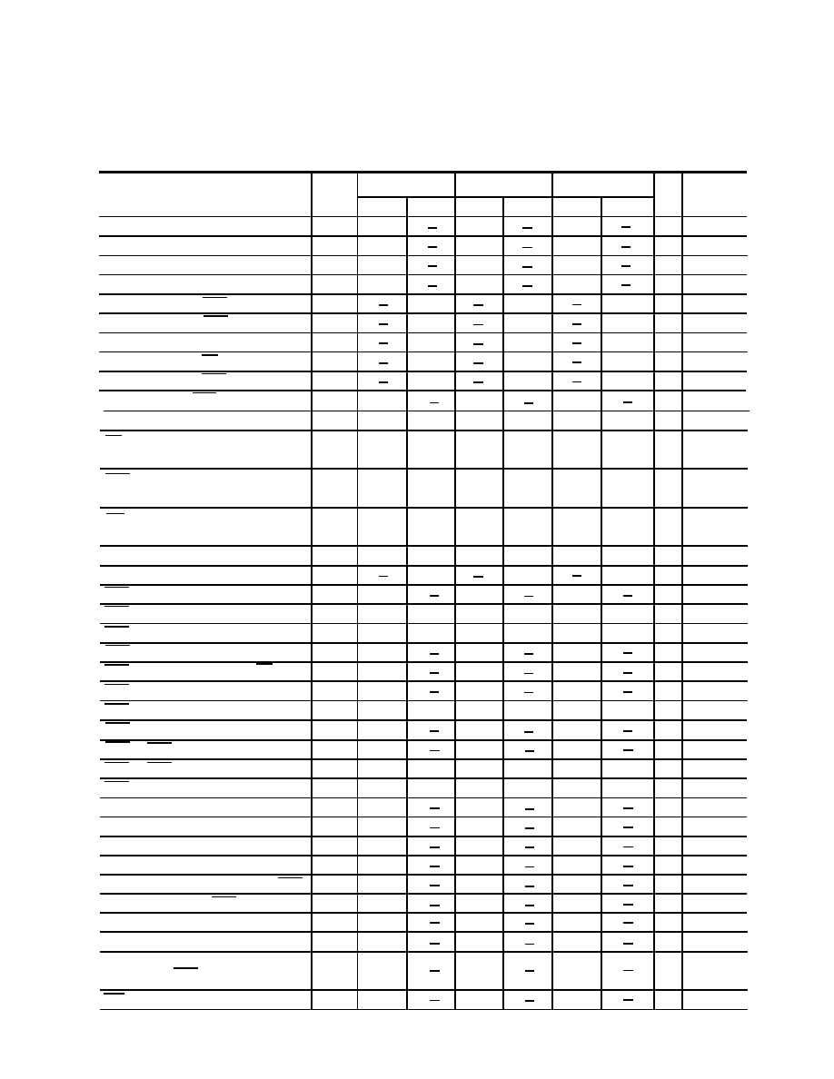
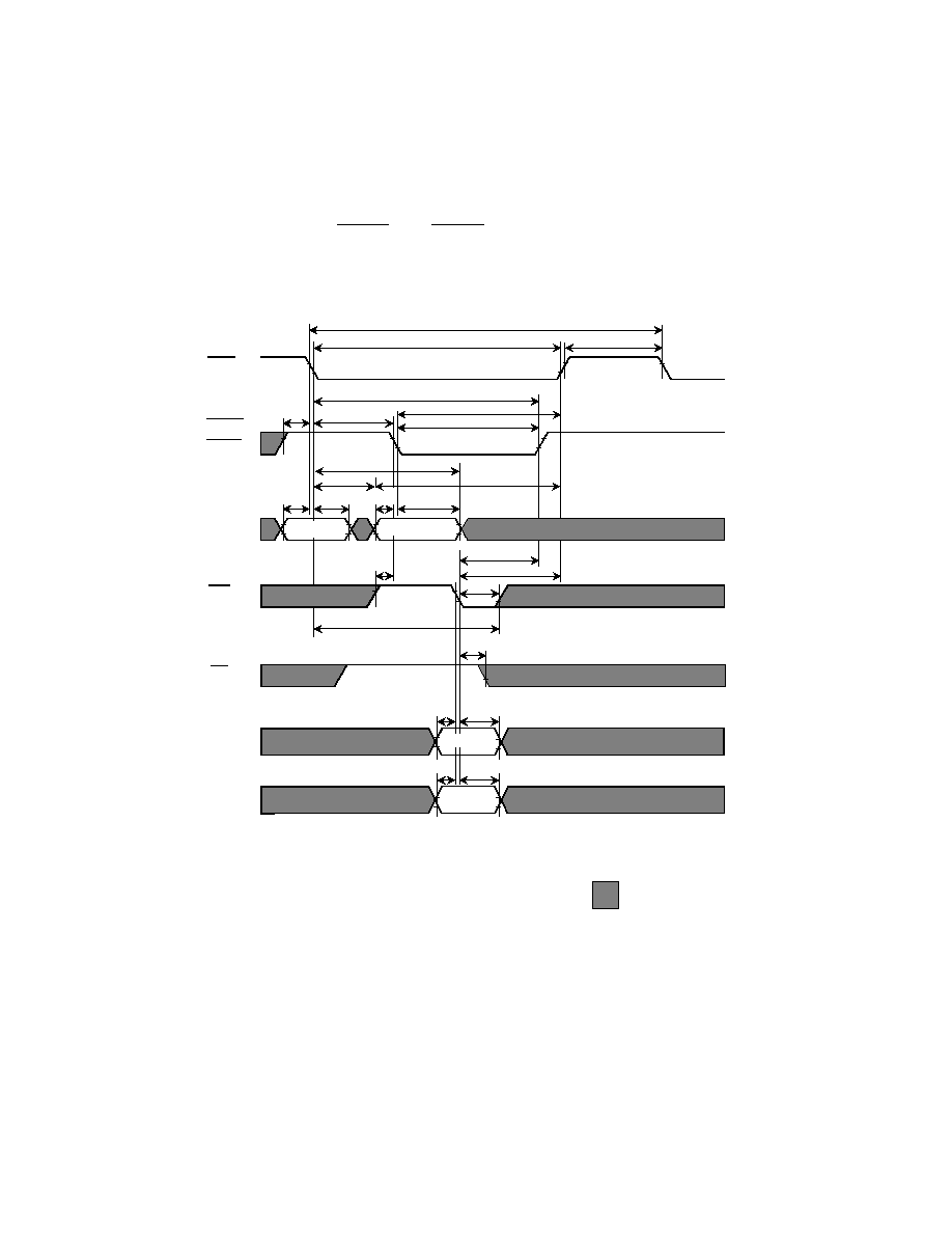
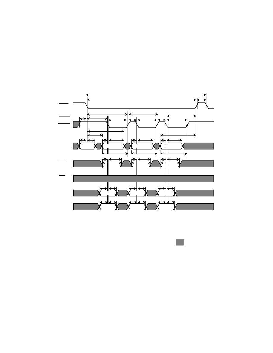
READ CYCLE (RAS output control )
RAS
RAS
A0-8
WE
DQ0-7
OE
ROW
COLUMN
tASR
tRAH
tASC
tCAH
tRAS
tRC
tRP
tRRH
tRCH
tCAC
tAA
tRAC
HZ
tOEA
tOEZ
tOFF
LCAS
tRCD
tCAS
tCSH
tRSH
tCRP
: "H" or "L"
tRAD
DQ8-15
VALID DATA
HZ
tOFF
tRCS
tRAL
tAR
tROH
UCAS
VALID DATA
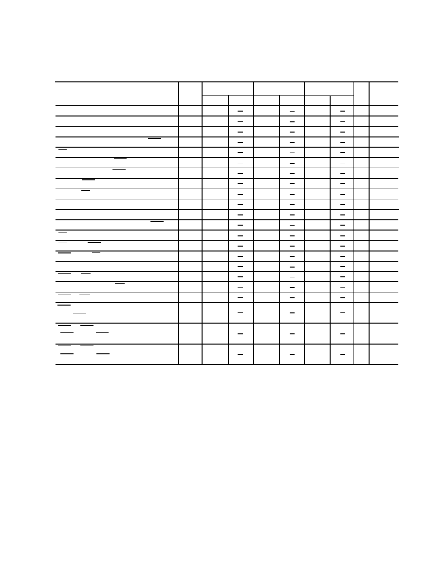
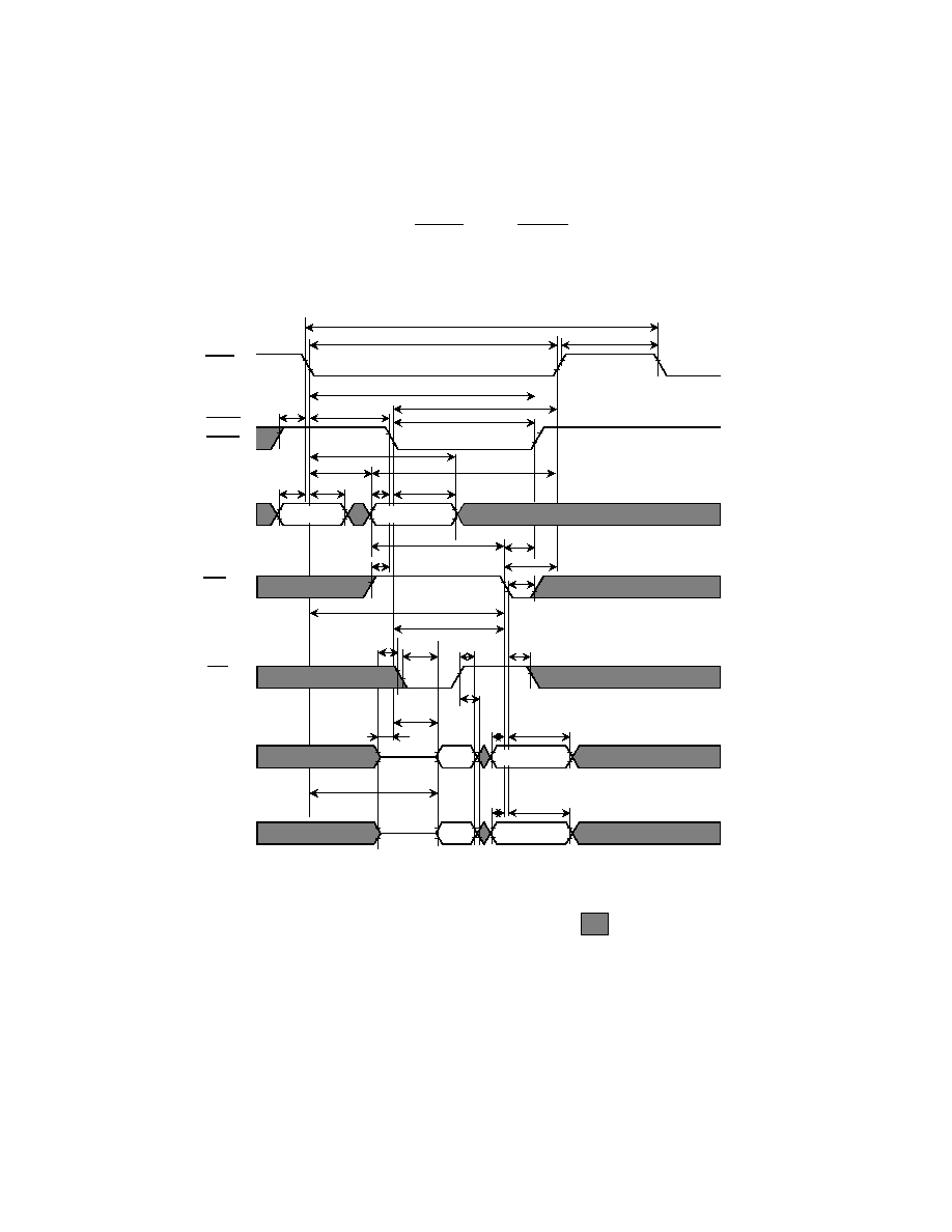
READ CYCLE (CAS output control )
RAS
A0-A8
DQ0-7
LCAS
OE
ROW
COLUMN
tASR
tRCD
tRAH
tASC
tCAH
tCAS
tRSH
tRAS
tRC
tRP
tCRP
VALID DATA
tCAC
tAA
HZ
tOEA
tOEZ
tOFF
tCSH
tRCS
: "H" or "L"
tRAD
DQ8-15
VALID DATA
tRAC
HZ
WE
tRRH
tROH
tRAL
tAR
UCAS
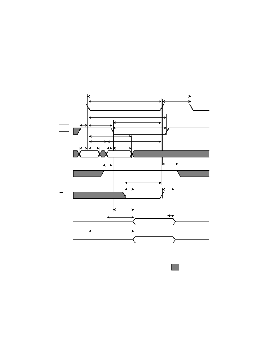
EARLY WRITE CYCLE (LCAS and UCAS active)
LCAS
RAS
A0-8
WE
DQ0-7
ROW
COLUMN
tASR
tRAH
tASC
tCAH
tRAS
tRC
tRP
OE
tCWL
tRWL
tWP
tWCR
tWCH
tRCD
tCAS
tCSH
tRSH
tCRP
DQ8-15
tWCS
: "H" or "L"
tRAD
VALID DATA
VALID DATA
tDH
tDS
tDH
tDS
tRAL
tAR
tDHR
UCAS
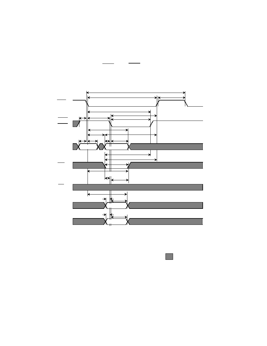
LATE WRITE CYCLE (LCAS and UCAS active)
RAS
A0-8
WE
DQ0-7
OE
ROW
COLUMN
tASR
tRAH
tASC
tCAH
tRAS
tRC
tRP
tOEH
tCWL
tRWL
tWCR
tRCS
tWP
: "H" or "L"
LCAS
tRCD
tCAS
tCSH
tRSH
tCRP
DQ8-15
tRAD
tDS tDH
tDS tDH
VALID DATA
VALID DATA
tRAL
tAR
UCAS
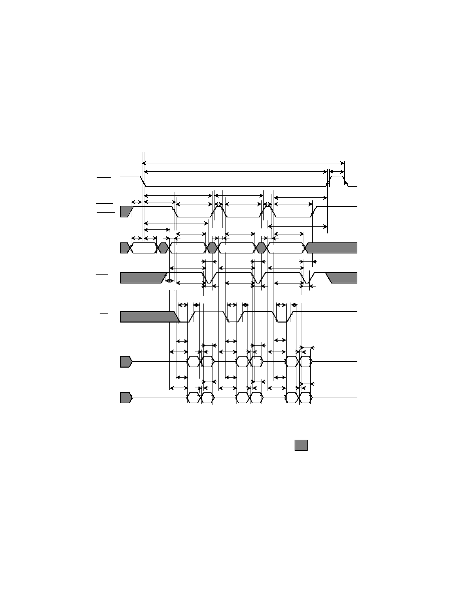
READ MODIFY WRITE CYCLE (LCAS and UCAS active)
RAS
A0-8
WE
DQ8-15
O
E
tASR
tRAH
tASC
tCAH
tRAS
tRMW
tRP
tAWD
tOEZ
OUT
tCWL
tRWL
tDS tDH
tRCS
tWP
tRWD
tRAC
tOEA
tOEH
tDZO
: "H" or "L"
LCAS
tRCD
tCAS
tCSH
tRSH
tCRP
DQ0-
7
OUT
tDS tDH
tDZC
tCAC
IN
IN
COLUMN
ROW
tRAD
tCWD
tRAL
tAR
UCAS
tOED
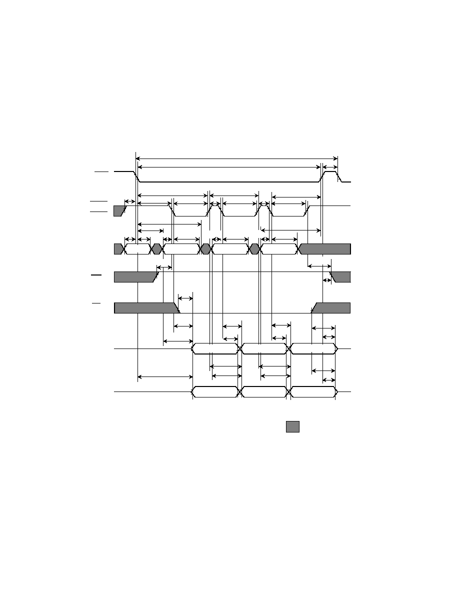
FAST PAGE MODE READ CYCLE with Extended Data Out
VALID DATA
tRP
RAS
tRASP
: "H" or "L"
A0-8
WE
ROW
COLUMN
tASR tRAH tASC
tCAH
tRCS
tRAD
tAR
COLUMN
tASC
tCAH
COLUMN
tCAH
tRAL
OE
tOEA
tASC
tRC
LCAS
tRCD
tCAS
tCSH
tRSH
tCRP
tCAS
tCAS
tPC
tCP
tCP
DQ8-15
VALID DATA
tRAC
HZ
tREZ
tAA
VALID DATA
tAA
DQ0-7
VALID DATA
tCAC
tAA
HZ
tREZ
tCAC
tCOH
tCPA
tCPA
tRRH
tRCH
tCAC
tCOH
UCAS
VALID DATA
VALID DATA
tOEZ
tOEZ
COLUMN
ROW
tASR
tRCD
tRAH
tASC
tCAH
tCSH
tRSH
tRASP
tCRP
: "H" or "L"
tAR
tASC
tCAH
tCAH
tHPC
tCP
tCP
tOEA
tCAC
tAA
tRAC
FAST PAGE MODE READ Hi-Z OPERATION
tASC
tRCS
tRC
COLUMN
COLUMN
VALID DATA
tDOH
tAA
tCPA
tOEA
tAA
tCRP
tRP
tCAS
tCAS
tCAS
tRAL
tRAD
tRRH
VALID
DATA
tOEZ
tOEP
tCHO
tOEP
tOEZ
tOCH
tOEA
tRCH
tWEP
tRCS
tCP
COLUMN
tASC
tWEZ
tCAH
tCAC
tCAC
tCAC
tAA
tCAS
tRCH
tREZ
RAS
LCAS
UCAS
A0-8
WE
OE
DQ0-7
DQ8-15
VALID DATA
VALID
DATA
VALID
DATA
VALID
DATA
VALID
DATA
VALID
DATA
VALID DATA
VALID DATA
FAST PAGE MODE EARLY WRITE CYCLE
RAS
A0-8
DQ0-7
OE
ROW
tASR tRAH tASC
tCAH
tRASP
tRP
: "H" or "L"
tRAD
tAR
tASC
tCAH
tCAH
tRAL
tASC
tRC
tDS tDH
tDS tDH
tDH
tDS
WE
tCWL
tWP
tWCH
tCWL
tWP
tWCH
tWCS
tCWL
tWP
tWCH
tWCS
LCAS
tRCD
tCAS
tCSH
tRSH
tCRP
tCAS
tCAS
tPC
tCP tCP
COLUMN
COLUMN
COLUMN
tWCS
DQ8-1
5
tDS tDH
tDS tDH
tDH
tDS
Input Data
Input Data
Input Data
Input Data
Input Data
Input Data
UCAS
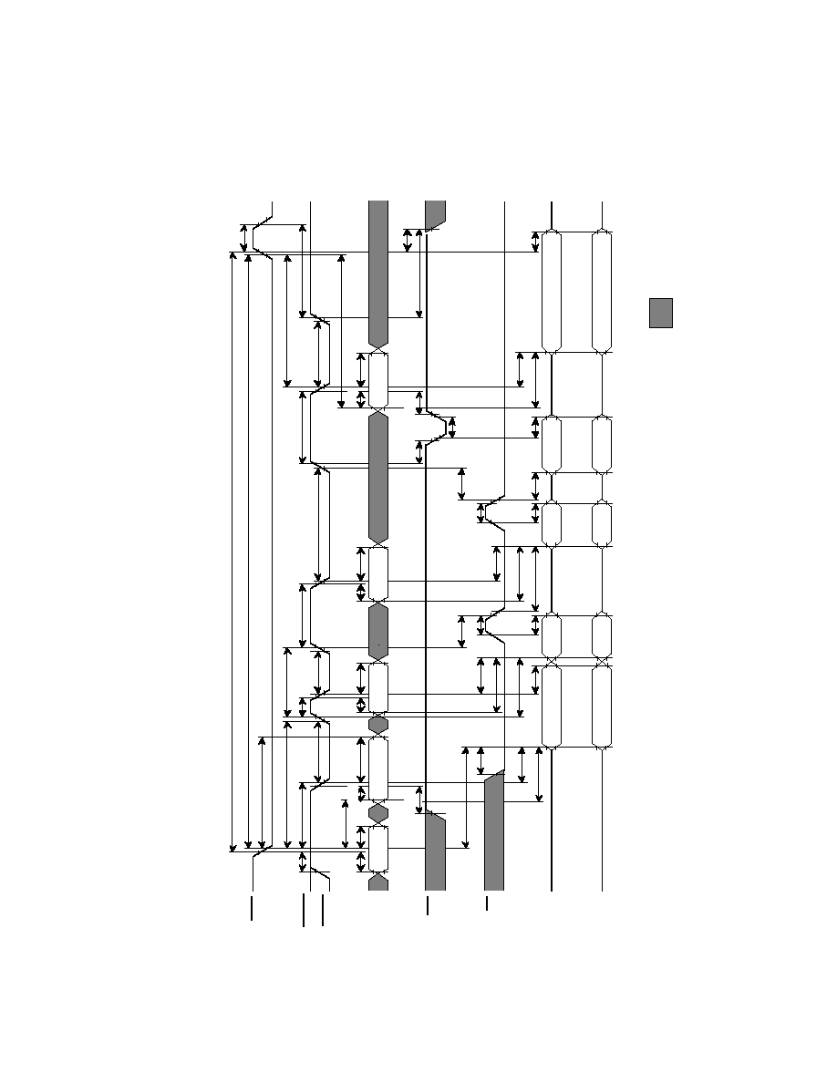
FAST PAGE MODE READ MODIFY WRITE CYCLE
IN
RAS
A0-8
WE
DQ0-7
OE
ROW
COLUMN
tASR tRAH tASC
tCAH
tRASP
tRP
tRAD
tAR
COLUMN
COLUMN
tRAL
tRC
@
@
tAWD
tRCS
tWP
tCWD
tCWL
tAWD
tWP
tCWD
tCWL
tAWD
tWP
tCWD
tCWL
tASC
tCAH
tASC
tCAH
tAA
tCAC
tDH
tDS
OUT
tAA
tCAC
tDS
tAA
tCAC
tDS
tDH
OUT
tDH
OUT
tOEA
tOEA
tOEZ
tOEZ
tOEA tOEZ
LCAS
tRCD
tCAS
tRSH
tCRP
tCAS
tCAS
tPRMW
tCP tCP
DQ8-15
tAA
tCAC
tDH
tDS
OUT IN
tAA
tCAC
tDS
tAA
tCAC
tDS
tDH
OUT IN
tDH
OUT IN
: "H" or "L"
UCAS
IN
IN
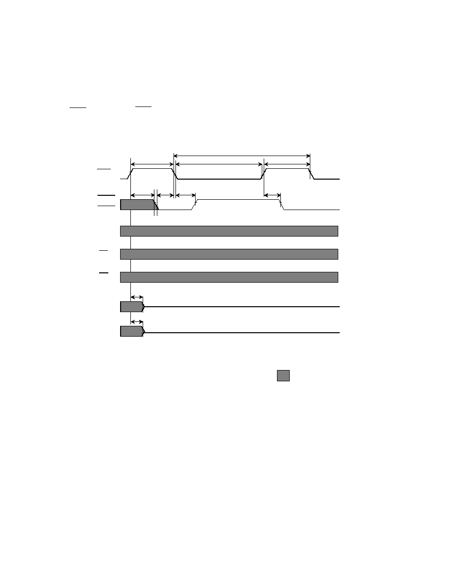
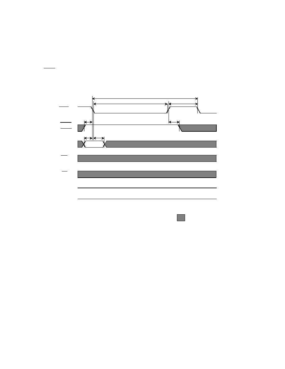
CAS BEFORE RAS REFRESH CYCLE
RAS
A0-8
WE
OE
tRAS
tRC
tRP
tOFF
tRP
: "H" or "L"
UCAS
tRPC
tRPC
tCSR
tCHR
DQ0-7
HZ
DQ8-15
HZ
tOFF
INHIBIT FALLING TRANSITION
LCAS
HIDDEN REFRESH CYCLE
RAS
A0-8
WE
DQ0-7
OE
VALID DATA
tCAC
tAA
tRAC
HZ
tOEA
tOEZ
ROW
tASR tRAH
tASC tCAH
tRAS
tRC
tRP
tRCS
tRRH
tRAD
tAR
tRAL
tRAS
tOFF
: "H" or "L"
UCAS
tRCD
tRSH
tCRP
tCHR
COLUMN
DQ8-15
VALID DATA
tCAC
tAA
tRAC
HZ
tOFF
LCAS
tROH
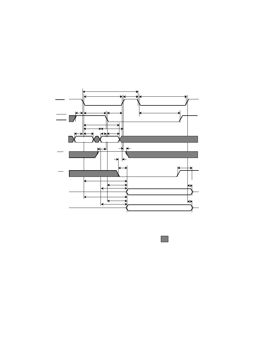
RAS ONLY REFRESH CYCLE
RAS
A0-8
WE
DQ0-7
OE
ROW
tRAH
tRAS
tRC
tRP
HZ
UCAS
tASR
tCRP
tRPC
DQ8-15
HZ
: "H" or "L"
LCAS
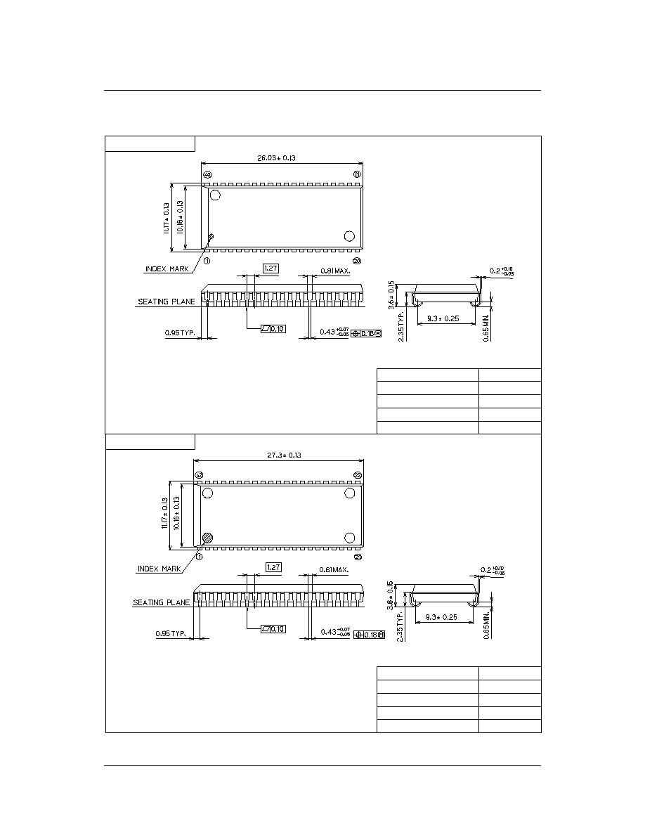
PACKAGE OUTLINES AND DIMENSIONS
20/20
Mirror finish
Mirror finish
SOJ40-P-400-1.27
(Unit: mm)
Package material
Lead frame material
Pin treatment
Solder plate thickness
Package weight (g)
Epoxy resin
42 alloy
Solder plating
5
mm or more
1.70 TYP.
SOJ42-P-400-1.27
Package material
Lead frame material
Pin treatment
Solder plate thickness
Package weight (g)
Epoxy resin
42 alloy
Solder plating
5
mm or more
1.86 TYP.